WIRELESS PARYLENE-BASED RETINAL
IMPLANT
Thesis by
Jay Han-Chieh Chang
In Partial Fulfillment of the Requirements for the Degree of
Doctor of Philosophy
California Institute of Technology
Pasadena, California
2014
© 2014
Jay Han-Chieh Chang
ACKNOWLEDGEMENTS
Foremost, I would like to express my sincere gratitude to my advisor Prof. Yu-Chong Tai for the
continuous support during my Ph.D. study and research, and for his patience, motivation, enthusiasm, and immense knowledge. His guidance helped me all throughout my research and writing of this
thesis. I could not have imagined having a better advisor and mentor for my Ph.D. study. It was an honor to have you as my advisor.
Besides my advisor, I would like to thank the rest of my candidacy and thesis defense committee: Prof. Hyuck Choo, Prof. Azita Emami, Prof. Joel Burdick, and Prof. James Weiland for their
encouragement, insightful comments, and hard questions.
I thank my fellow labmates in the Caltech MEMS Group, in particular Dr. Bo Lu, Dr. Ray Huang, Dr. Jeffrey Chun-Hui Lin, and Dr. Mike Liu; thank you for mentoring and training me when I was in
the earlier years of my research career in the lab, and enlightening me on the first glance of research. To the rest of the members, Dr. John Chen, Dr. Luca Giacchino, Dr. Justin Young-Hyun Kim, Dr.
Wendian Shi, Dr. Charles Deboer, Mandheerej Nandra, Yu Zhao, Zhao Liu, Dongyang Kang, Yang
Liu, Shell Zhang, and Nick Scianmarello: thank you for your support, generous assistance, stimulating discussions, and brilliant ideas. The lab would not have been this organized and efficient
if it were not for the collaboration and hard work from each and every one of you. Special credit must be given to Yang Liu and Shell Zhang, who helped on the device fabrication and electroplating
setup.
My great appreciation also goes to Christine Garske and Tanya Owen, thank you for your help in
purchasing and administrative tasks. You have made the lives of all members in the lab so much
Many thanks go to the PI of the project, Dr. James Weiland and Dr. Mark Humayun, who have
invested their full effort in guiding the team in achieving the goal. I have to appreciate the guidance given by them. I also appreciate my USC co-workers, including Dr. Yi Zhang, Dr. Artin Petrossians,
and Dr. Alice Cho, who have dedicated their time and effort in advancing the research program in both USC and Caltech and have helped me tremendously in my research endeavor in BMES ERC;
my UCLA co-workers including Dr. Wen-Tai Liu, Dr. Kuan-Fu Chen, and Yi-Kai Lo, who
developed many generations of retinal IC chips for the project; my Caltech co-workers, including Dr. Azita Emami, and Manuel Monge, who also developed retinal IC chip for the project and helped on
the measurement of parylene-chip integration.
Last but not the least, I would like to thank my parents, who have always been there for me and
have given me unconditional support over the years in every aspect of my life. Most importantly,
ABSTRACT
Wireless Parylene-Based Retinal Implant
Thesis by
Jay Han-Chieh Chang
Doctor of Philosophy in Electrical Engineering California Institute of Technology
The degeneration of the outer retina usually causes blindness by affecting the photoreceptor cells. However, the ganglion cells, which consist of optic nerves, on the middle and inner retina layers are
often intact. The retinal implant, which can partially restore vision by electrical stimulation, soon becomes a focus for research. Although many groups worldwide have spent a lot of effort on
building devices for retinal implant, current state-of-the-art technologies still lack a reliable packaging scheme for devices with desirable high-density multi-channel features. Wireless flexible
retinal implants have always been the ultimate goal for retinal prosthesis. In this dissertation, the
reliable packaging scheme for a wireless flexible parylene-based retinal implants has been well developed. It can not only provide stable electrical and mechanical connections to the high-density
multi-channel (1000+ channels on 5 mm × 5 mm chip area) IC chips, but also survive for more than 10 years in the human body with corrosive fluids.
The device is based on a parylene-metal-parylene sandwich structure. In which, the adhesion
between the parylene layers and the metals embedded in the parylene layers have been studied.
schemes have been tried in application to IC chips and discrete components to gain the longest
lifetime. The effectiveness has been confirmed by the accelerated and active lifetime soaking test in saline solution. Surgical mockups have also been designed and successfully implanted inside dog's
and pig's eyes. Additionally, the electrodes used to stimulate the ganglion cells have been modified to lower the interface impedance and shaped to better fit the retina. Finally, all the developed
technologies have been applied on the final device with a dual-metal-layer structure.
TABLE OF CONTENTS
ACKNOWLEDGEMENTS...iii
ABSTRACT...v
TABLE OF CONTENTS...vii
LIST OF FIGURES...xi
LIST OF TABLES...xx
GLOSSARY...xxi
1. INTRODUCTION...1
1.1 RETINAL PROSTHESIS...1
1.2 MEMS TECHNOLOGY...4
1.2.1 PHOTOLITHOGRAPHY...8
1.2.2 BULK MICROMACHINING...9
1.2.2.1 WET ETCHING...9
1.2.2.2 DRY ETCHING...11
1.2.3 SURFACE MICROMACHINING...13
1.2.4 HIGH-ASPECT-RATION MICROMACHINING...14
1.2.4.1 LIGA...14
1.2.4.2 LASER MICROMACHINING...16
1.3 PARYLENE...16
1.4 INTEGRATION TECHNOLOGY...20
1.4.1 TRADITIONAL CHIP INTEGRATION TECHNOLOGY...20
1.4.2 STATE-OF-THE-ART CHIP INTEGRATION TECHNOLOGY...23
1.4.2.2 BOSTON RETINAL IMPLANT PROJECT...25
1.4.2.3 CALIFORNIA INSTITUTE OF TECHNOLOGY-CL-I2 ...27
1.5 LAYOUT OF THE DISSERTATION...29
1.6 SUMMARY...29
1.7 REFERENCE...30
2. HIGH-DENSITY MULTI-CHANNEL CHIP INTEGRATION...34
2.1 INTRODUCTION...34
2.2 OVERVIEW OF REQUIREMENTS FOR DEVICE PACKAGING...36
2.3 DEVICE DESIGN...38
2.3.1 METALS...38
2.3.2 FIRST–GENERATION PARYLENE-C FLEX FABRICATION...41
2.3.3 SECOND-GENERATION PARYLENE-C FLEX FABRICATION...42
2.4 DEVICE PACKAGING...43
2.4.1 ALIGNMENT AND SQUEEGEE...43
2.4.2 SQUEEGEE ISSUES...45
2.4.3 LASER CUTTING...48
2.4.4 DEVICE TESTING...50
2.5 ADHESION-ENHANCEMENT SURFACE TREATMENT...51
2.5.1 DEVICE DESIGN AND FABRICATION...51
2.5.2 EXPERIMENTS AND RESULTS...55
2.5.2.1 PEELING TEST...55
2.5.2.2 SOAKING TEST...58
2.6 DRY MECHANICAL LIFTOFF TECHNOLOGY...60
2.6.1 DESIGN OF SOAKING SAMPLES...63
2.6.3 FABRICATION PROCESS...65
2.6.4 DISCUSSION...69
2.6.4.1 SU-8 THICKNESS...69
2.6.4.2 SMALLEST FEATURE...69
2.6.4.3 COMPARISON OF RESISTANCE...69
2.7 SUMMARY...71
2.8 REFERENCE...72
3. PHOTO-PATTERNABLE ADHESIVES AND THEIR APPLICATIONS...75
3.1 INTRODUCTION...75
3.2 MOTIVATION...76
3.3 INVESTIGATION OF PHOTO-PATTERNABLE ADHESIVES...78
3.3.1 EXPERIMENTAL PROCEDURE AND SETUP...78
3.3.2 RESULTS AND DISCUSSION...81
3.4 APPLICATIONS ON HIGH-DENSITY MULTI-CHANNEL CHIP INTEGRATION...85
3.4.1 YIELD TEST...88
3.4.2 LIMITS OF THE PROPOSED TECHNOLOGY...91
3.5 REAL CHIP FUNCTIONAL TESTING...93
3.5.1 TESTING ON 268-CHANNEL CHIP INTEGRATION...95
3.5.2 TESTING ON 1024-CHANNEL CHIP INTEGRATION...98
3.6 SUMMARY...102
3.7 REFERENCE...104
4. LIFETIME STUDY OF PACKAGING AND SURGICAL MOCKUP...106
4.1 INTRODUCTION...106
4.2 LIFETIME STUDY AND ANALYSIS...110
4.2.2 EXPERIMENTAL RESULTS...117
4.3 SURGICAL MOCKUP DESIGN AND IN VIVO TEST...130
4.3.1 512-CHANNEL CHIP...130
4.3.1.1 THE 3-COIL WIRELESS POWER TRANSFER...130
4.3.1.2 SIMULATION OF THE INTERFERENCE BETWEEN COILS...131
4.3.1.3 THE FLEXIBLE MECHANICAL MODEL...133
4.3.2 1024-CHANNEL CHIP...136
4.3.3 MAXIMUM PULLING FORCE...142
4.4 SUMMARY...144
4.5 REFERENCE...146
5. 1024-CHANNEL RETINAL PROSTHESIS...148
5.1 INTRODUCTION...148
5.2 DEVICE DESIGN...150
5.3 MULTI-ELECTRODE ARRAY (MEA)...154
5.3.1 ELECTROPLATING...154
5.3.2 THERMOFORMING...162
5.4 INTEGRATION OF IC CHIP, DISCRETE COMPONENTS, AND COILS...164
LIST OF FIGURES
Figure 1.1. Diagram of the human eyeball structure...2
Figure 1.2. System overview and comparison of locations of epiretinal and subretinal implants...3
Figure 1.3. Basic components of the retinal implant system...4
Figure 1.4. Complexity of MEMS device by structure layers...5
Figure 1.5. Comparison of the fabrication process between positive and negative photoresist...9
Figure 1.6. Comparison of the bulk micromachining process: (a) Anisotropic etching. (b) Isotropic etching. (c) RIE...11
Figure 1.7. Electrostatic comb-drive actuator fabricated by Deep Reactive Ion Etching (DRIE) of silicon-on-insulator (SOI) wafer...12
Figure 1.8. Comparison of bulk micromachining and surface micromachining in cross-sectional view. ...12
Figure 1.9. (Left) Illustration of surface micromachining process. (Right) Polysilicon micromotor fabricated using a surface micromachining process...14
Figure 1.10. LIGA process: (a) Exposure. (b) Electroplating. (c) Finishing to height. (d) Removal of the substrate...15
Figure 1.11. Chemical structure of Parylene-N, -C, -D, and-HT and the process temperature...17
Figure 1.12. Illustration of the deposition system of Parylene and the process flow...19
Figure 1.13. Demonstration of soldering...21
Figure 1.14. Demonstration of wire bonding...22
Figure 1.15. Demonstration of the process of flip chip assembly...23
Figure 1.16. (Left) Overview of the Microflex technique. (Right) SEM pictures of the contact array. ...25
chip are placed on the eyeball. The electrode array is placed in the subretinal space through a scleral flap...27
Figure 1.19. (Left) Illustration of the CL-I2 packaging concept. (Right) Concept of embedded chip
integration...28 Figure 2.1. Parylene cracks occur on the edges of the metal lines, resulting in solution attack and causing delamination...36 Figure 2.2. Requirements for packaging issues for a wirelessly flexible parylene-based retinal implant device…...38 Figure 2.3. Lift-off process flow on parylene substrate...40 Figure 2.4. Comparison of patterns on sample after development without (Left) and with (Right) undercut...40 Figure 2.5. Fabrication process flow of the first-generation parylene-C flex...41 Figure 2.6. Fabrication process flow of the second-generation parylene-C flex...43
Figure 2.7. Alignment of the bonding pads with the metal pads on the chip. Alignment accuracy of
10µm can be achieved...45
Figure 2.8. Squeegee process: after alignment, the rubber squeegee is used to push the excess
conductive epoxy away from the surface into the wells to make connections between parylene flex and chips...45
Figure 2.9. (Left) Add a layer of patternable epoxy to increase the aspect ratio. (Right) Footprint on a testing substrate with SU-8 wall after squeegee process...46 Figure 2.10. (Left) The surface of the bonding pads after squeegee and surface cleaning. (Right) The surface profile of the bonded conductive epoxy; average height is around 20 µm...47 Figure 2.11. (Left) Edge of the chip where the squeegee process may become a problem. (Right) PDMS mold fitted with a 256 channel stimulation chip...48
Figure 2.12. (Left) Short circuit defects on dense metal lines. (Right) Short circuit defects repair
process...49
Figure 2.13. (Left) Shortage of neighboring metal pads underneath the parylene film due to low
viscosity of the conductive epoxy. (Right) Electrically isolate the neighboring pads after UV laser cleaning...50
Figure 2.15. Process steps of different treatments: (Top) treatment for interface of silicon and parylene. (Bottom) Treatment for interface of parylene and parylene...52 Figure 2.16. Sample layouts for peeling tests. (Left) Peeling test between parylene and silicon. (Right) Peeling test between parylene and parylene...53 Figure 2.17. Sample layouts for soaking tests (a) between parylene and silicon and (b) between parylene and parylene. (c) Fabricated sample for soaking test. (Bottom right) 0.9 wt% NaCl solution...54
Figure 2.18. (Left) Fabricated sample with sacrificial PR for peeling test. (Right) Partially released
Figure 3.1. Former connection technology that requires an additional PDMS holder to house the IC chips; the adhesion between parylene-C and chips only relies on conductive epoxy, which occupies
less than 2% of the total contacting area...78
Figure 3.2. Schematic representation of a clamp as the bonding tool on the testing samples...79
Figure 3.3. Cross-sectional SEM image of the adhesive bonding between parylene sheet and silicon (2MPa, 130ºC). The shape of the microstructure keeps the same after the bonding process and the bonding pads are well defined...80
Figure 3.4. (a) Setup of the force gauge to measure the peeling force. (b) Real testing sample after bonding. (c) Schematic representation of the testing sample with top view and cross-sectional view...81
Figure 3.5. Peeling force v.s. bonding temperature for various photo-patternable adhesives...82
Figure 3.6. Peeling force v.s. bonding pressure for various photo-patternable adhesives...83
Figure 3.7. Adhesive interface before (a) and after (b) peeling test...84
Figure 3.8. (a) Maximum peeling forces of different photo-patternable adhesives. (b) Peeling force v.s. bonding time for different photo-patternable adhesives...85
Figure 3.9. Custom holder for chip assembly technique; all lithography was done on this holder which also served as the safety buffer zone for squeegee...86
Figure 3.10. (a) Dummy chip for assembly yield test; pads also served as alignment marks. (b)&(c) Metal pads were exposed; resolution of around 5μm could be achieved...86
Figure 3.11. (a) Unbaked AZ4620. (b) AZ4620 baked at 140°C for 30 minutes in vacuum oven; slope formed by reflow will be beneficial for conductive epoxy to be fed through. (c)&(d) Side lengths show no change before and after baking...87
Figure 3.12. Gluing area was increased from 2% to 94% (2%+92%) by the extra photoresist used as glue. Note that unnecessary pads were covered to avoid shortage...88
Figure 3.13. (a) Dummy chip and discrete components integrated with surgical parylene flex. (b) Backside of the dummy chip and discrete components. (c) Close-up view of the high-density multi-channel chip integration. (d) Retinal tack used to fix stimulating electrodes on retina...89
Figure 3.14. Setup of the measurement; the electrode array outputs (the electrode end that will be placed on macula) were probed to check the connection...90
Figure 3.16. (a) Dummy chips with 40μm by 40μm pad size and 40μm separation. (b) Connection between parylene substrate and dummy chip. (c) Yield v.s. separation of pads. (d) Yield v.s. side length of pads. The results show that high connection yield (>90%) can be achieved for pads as small as 40μm by 40μm and with a 40μm separation in between...92 Figure 3.17. (a) Surgical parylene-C device connected with silicon chip and discrete components. (b)(c) Only desired metal pads are exposed; other area is covered by photo-patternable adhesives. The alignment accuracy can be improved to be around 5 µm...94
Figure 3.18. Gluing area is increased from 2% to 94 (2+92)%. Unnecessary pads are also covered to
avoid electrical shortage during conductive epoxy squeegee process...95
Figure 3.19. Layout and wiring diagram of the real 268-channel retinal IC chip...96
Figure 3.20. Only desired metal pads were exposed; other area and pads for testing only were covered by photo-patternable adhesives...97
Figure 3.21. (a) Real 268-channel retinal IC chip integration by photo-patternable adhesives and conductive epoxy squeegee techniques. (b) Successful functional signal testing including oscillator assembly, clock level shifter, and low voltage rectifier...97
Figure 3.22. Layout and wiring diagram of the real 1024-channel retinal IC chip...99
Figure 3.23. Parylene flex integrated with 1024-channel retinal IC chip, and the connection of
critical pads can be seen very clearly...100
Figure 3.24. The tested power coil from USC (center-tapped receiver coil) has similar inductance ratio and better Q factor compared to the litz-wire coil used in UCLA's demo system. It can successfully induce correct voltages for the 1024 channel retinal IC chip and was used as the power coil for the whole system...100 Figure 3.25. With correct induced voltage from the receiver power coil, all correct DC voltages including VrddL, VrddH, VrssL, and VrssH were successfully tested via wires through parylene flex with high yield...101 Figure 3.26. With correct induced voltage from the receiver power coil, the crystal oscillator output with 16MHz signal was successfully tested via wires through parylene flex with high yield...102 Figure 4.1. (Left) Parylene-based device protected by traditional silicone-parylene combination. (Right)Parylene-based device protected by the proposed parylene-metal-parylene protection scheme...108
Figure 4.2. Schematic representation of the retinal implant connected with IC chips, coils, and
discrete components...108
Figure 4.4. Commercial amplifier chips, discrete components, and resistor chips were first integrated and packaged before soaking test...111 Figure 4.5. Fabrication process of the parylene-C pocket structure. The sacrificial area is designed to be 2 mm×2 mm to accommodate the bare die (1.6mm×1.1mm×200 µm) and it leaves some space for chip insertion and movement. The pocket structure can provide support to the chip to make alignment...113 Figure 4.6. Schematics of the process flow to show how to open pocket and insert chip...113
Figure 4.7. Parylene pocket is opened by spatula after releasing the sacrificial photoresist. With
wafer dicing tape as a fixation substrate, the pocket becomes easier to open...114
Figure 4.8. (a) A chip is inserted and aligned; conductive epoxy is applied to make connection. (b)
Alignment accuracy of 10µm can be achieved. (c) The size of conductive epoxy drop is 200µm in diameter. (d) Signal is monitored by oscilloscope...114
Figure 4.9. (a) Top side of the series RLC circuit built by discrete components. (b) Resonant frequency is measured by impedance analyzer...115 Figure 4.10. Measurement setup of active soaking test for dummy conduction chip. Power supply, multi-meter, and dummy conduction chip soaked in saline are arranged in series. Door is opened to show the setup inside...116 Figure 4.11. Line resistance v.s. time of samples coated by 40µm parylene-C only soaked in high temperature saline solution. The subset shows the difference of chip size of dummy conduction chips...117 Figure 4.12. (a) After sandwich layer protection, the device is still highly flexible. (b) Device becomes inflexible after coating with thick silicone; thickness needs to be more than 5mm...118 Figure 4.13. Schematics of proposed packaging scheme and other protection for comparison...119 Figure 4.14. High-density multi-channel chip integration protected by different packaging schemes. (Top left) No protection; (Top right) 40 µm parylene-C only; (Bottom left) 5mm silicone + 40 µm parylene-C; (Bottom right) 20 µm parylene-C + 0.5 µm metal + 20 µm parylene-C...120 Figure 4.15. Observed failure modes, including bubbles and corrosion, on parylene devices (a), corrosion of sandwiched metals (b), delamination of metal traces on dummy chips (c), and corrosion of conductive epoxy (d), respectively, are found after soaking...121
Figure 4.16. Samples without protection, water vapor can penetrate the thin parylene layer of device
itself to damage the metals very quickly, especially under a bias field...122
Figure 4.17. Samples with thick parylene and other protection, uniform bubbles around the whole
device are first observed and water vapor gradually diffuses through the protection to attack the device...122
Figure 5.15. (Left) Impedance model. (Right) Impedance on Nyquist plot...160 Figure 5.16. Nyquist plot of the impedance before (Left) and after (Right) plating...161 Figure 5.17. Randles circuit model for electrode/electrolyte interface. W.E.: working electrode; R.E.: reference electrode; C.E.: counter electrode...162 Figure 5.18. (Left) Schematic of the mold used to shape the electrodes to fit the retina. (Right) Real picture of the final mold...163 Figure 5.19. (Left) Electrodes were shaped by the mold. (Right) After shaping, the electrodes were well shaped...163 Figure 5.20. Conductive epoxy squeegee technique built for high-density multi-channel chip...165 Figure 5.21. Discrete components and coils with bigger bonding pads were connected by conductive epoxy using needles...165 Figure 5.22. Front side and back side of the integration after protection coating...166
Figure 5.23. Complete flow illustrating how to build a wirelessly flexible parylene-based retinal implant device...166
LIST OF TABLES
Table 1.1. Important properties of Parylene-N, -C, -D, -HT, and PDMS...19 Table 2.1. Maximum force readings of the peeling test (n=5)...57 Table 2.2. Soaking tests (n=5) to observe undercut and vertical attack bubble density (V.A.B.D.)...59 Table 2.3. The estimated time of the wet process...62 Table 2.4. Undercut rate of the samples soaked in high temperature saline by different interface treatments (μm/day)...65 Table 4.1. Water vapor transmission rate (WVTR) of common materials used to protect parylene-based device...106 Table 4.2. MTTF of various tested samples are recorded and calculated to estimate the lifetime at 37°C under different protections (a)...123 Table 4.3. Thermal conductivity of the materials...125 Table 4.4. MTTF of various tested samples are recorded and calculated to estimate the lifetime at 37°C under different protections (b)...129
CLOSSARY
AMD – age-related macular degeneration
ASCII – American Standard Code for Information Interchange ASIC – Application Specific Integrated Circuit
ASTM – American Society for Testing and Materials
BGA – ball grid array
CL-I2– Chip-level Integrated Interconnect
CMOS – complementary metal–oxide–semiconductor CT – computed tomography
CVD – chemical vapor deposition
DIP – dual in-line package DRIE – deep reactive ion etching
EDM – electric discharge machining EDP – ethylene diamine pyrocatechol
FDA – Food and Drug Administration
HARM – high-aspect-ratio micromachining HF – hydrofluoric acid
HNA – hydrofluoric acid, nitric acid and acetic acid IC – integrated circuit
ID – identification
ISO – International Organization for Standardization
KOH – potassium hydroxide
Molding)
LOR – lift-off resist
MEMS – micro-electro-mechanical systems
MFI – MicroFlex interconnect MRI – magnetic resonance imaging
MTTF – mean time to failure
PCB – printed circuit board PDMS – polydimethylsiloxane
PR – photoresist
PSG – phosphosilicate glass
RF – radio frequency
RFID – radio frequency identification RIE – reactive ion etching
RLC – resistor-inductor-capacitor RP – retinitis pigmentosa
SAP – silicone adhesion promoter SEM – scanning electron microscope
SNR – signal-to-noise ratio
SOI – silicon on insulator
TMAH – tetramethylammonium hydroxide
TTL – transistor-transistor logic USP – United States Pharmacopeia
WHO – World Health Organization
1 INTRODUCTION
1.1
Retinal Prosthesis
In normal human vision, as shown in Figure 1.1, the light enters the eye through the cornea, the pupil, and is focused by the transparent crystalline lens. The light then goes through the vitreous
body which is filled with vitreous humor, through the layers of the inner retina, and it is ultimately
focused onto the photoreceptors of the outer retina. Along the pathway, the delicate retina performs significant visual processing works. According to the World Health Organization (WHO), the two
most common leading causes of blindness induced by degenerative retinal diseases are the age-related macular degeneration (AMD) and retinitis pigmentosa (RP). The defects will damage the
outer photoreceptors and cause the loss of the cone and rod receptors in the eye. Blindness due to
such outer retinal diseases have affected several million people in the world. In fact, it has been estimated by The Eye Diseases Prevalence Research Group and the National Eye Institute that AMD
alone will affect more than three million people in the United States by the year 2020 [1]. In addition, the prevalence of RP has been estimated to be approximately 1 in 4000 [2]. Recent evidence has
shown that gene, drug, and nutrition therapies could be some possibilities for the treatment of such diseases [3-4]. However, such treatments, in reality, are still very far away from being used in
clinical practice, and have a number of ethical and political barriers to their implementation.
Therefore, blindness still cannot be treated in the end.
In 1994, Dr. Humayun et al. reported the results to electrically stimulate vertebrate retinas [5] as
another possible treatment for these retinal diseases. The main idea is to bypass the damaged photoreceptors in the normal visual route. In this study, damaged bullfrog eyecups and rabbit eyes,
retinal response. The ganglion cell layers which consist of optical nerves can be electrically
[image:24.595.160.454.209.434.2]stimulated to construct localized vision signals in patients [6-9]. This is so called “Retinal Prosthesis”, a possible treatment for patients with devastating blindness due to outer retinal disease.
Figure 1.1. Diagram of the human eyeball structure. (Image courtesy from www.glogster.com)
There are now a large variety of approaches to artificial vision, each with their own advantages and disadvantages. Among them, the main stimulation schemes are epiretinal and subretinal
approaches, which differ by the location of the implanted devices and stimulation sites. For the
epiretinal approach, as shown in Figure 1.2, an electrode array is placed directly on the retina from its anterior aspect. For the subretinal approach, an electrode or photodiode array is placed within the
layers of the retina [10]. The state-of-the-art epiretinal prosthesis has been successfully demonstrated as a prototype of 60-electrode device, developed by Second Sight Medical Products, Inc. in patients
environment free from background distracters, which is already a huge achievement of engineering
and medicine. Furthermore, subjects have been shown to be able to determine direction of movement of parallel white bars on a black background, as well as locate white squares within a quadrant of
otherwise black space [12]. Also, patients have demonstrated their ability to read large letters simply by scanning the camera mounted on their head back and forth over the image displayed in front of
[image:25.595.122.494.284.553.2]them.
Figure 1.2. System overview and comparison of locations of epiretinal and subretinal implants [13].
The basic components of the retinal prosthesis system are almost the same, as shown in Figure 1.3: an external camera is mounted on a glass to take videos and pictures to general the raw signals.
The signals will be then wirelessly sent into the eye and further analyzed by internal circuitry to
Figure 1.3. Basic components for the retinal implant system. (Image courtesy from www.thinfilmsblog.com)
1.2 MEMS Technology
Micro-electro-mechanical system (MEMS), the acronym which originated in the United States, is
also referred to as Microsystems Technology (MST) in Europe and Micromachines in Japan. MEMS
is a fabrication technology applied to build small integrated devices and systems that consist of both mechanical and electrical components [14-15]. Because of its root in the IC industry, MEMS devices
are fabricated using integrated circuit (IC) batch processing techniques and typically can range from 0.1 to 100 micrometer in sizes. Usually, these devices are able to detect, control and actuate on the
micro scale, and response on the macro scale. Fabrication processes such as bulk and surface
integrated circuits (IC) are designed and fabricated to take advantages of the electrical properties of
the silicon, MEMS technology exploits both its electrical and mechanical properties, thus resulting in broader application. MEMS is an integrated technology in micro-scale. It can consist of many
microstructures, such as sensors, actuators, and electronics, all of them are integrated onto single silicon substrate. Among them, sensors can first detect the changes in the system’s environment by
measuring the mechanical, thermal, magnetic, chemical or electromagnetic data and phenomena.
Electronics can then process this information. After that, the actuators can react and create some form of changes to the environment. In addition, MEMS devices are usually very small, and their
components are usually in micro scale. Levers, gears, pistons, and motors have all been fabricated by MEMS technology. Figure 1.4 shows a potential complexity of MEMS system with the addition of
[image:27.595.90.531.396.600.2]independently-structured layers.
Figure 1.4. Complexity of MEMS device by structure layers [15].
MEMS has many diverse advantages, in micro-scale, as a fabrication technology. Many previously unrelated fields have been connected together by the interdisciplinary nature of MEMS
devices to be more stable and reliable. In addition, MEMS provides the foundation for the
manufacture technology of products that cannot be replaced by other methods. All these factors make MEMS potentially a more popular and broader technology than integrated circuit (IC) microchips
technology. However, there are still many challenges and technological difficulties associated with the miniaturization that need to be studied and overcome before MEMS technology can really realize
its overwhelming potential around the world.
When it comes to the history of MEMS, from a very early vision in the early 1950’s, MEMS has gradually made its way out of research laboratories and into everyday products. In the mid-1990’s,
MEMS components began to appear in numerous commercial products and applications including accelerometers used to control airbag in vehicles, pressure sensors for medical applications, and
inkjet printer heads. Today, MEMS devices are also found in projection displays and used for
micropositioners in data storage systems. However, the most important potential for MEMS devices lies in the new applications on the biomedical and process control areas.
The following lists the major history of MEMS which is useful to show its diversity, challenges, and application [16]:
1947 Realization of transistors.
1958 Silicon strain gauges commercially available.
1959 “There’s Plenty of Room at the Bottom” – Richard Feynman gives a milestone presentation at California Institute of Technology.
1961 First silicon pressure sensor demonstrated.
1967 Invention of surface micromachining. Westinghouse creates the Resonant Gate Field Effect
Transistor, (RGT). Description of use of sacrificial material to free micromechanical devices from the silicon substrate.
1979 First micromachined inkjet nozzle demonstrated.
1982 Disposable blood pressure transducer demonstrated.
1982 “Silicon as a Mechanical Material” [17]. Instrumental paper to entice the scientific
community – reference for material properties and etching data for silicon. 1982 LIGA Process.
1988 First MEMS conference held.
1992 MCNC starts the Multi-User MEMS Process (MUMPS) sponsored by Defense Advanced Research Projects Agency (DARPA).
1992 First micromachined hinge demonstrated.
1993 First surface micromachined accelerometer sold (Analog Devices, ADXL50).
1994 Deep Reactive Ion Etching is patented.
1995 BioMEMS rapidly develops.
2000 MEMS optical-networking components become big business.
MEMS can be further divided into three different classifications; bulk micromachining, surface
micromachining, and high-aspect-ratio micromachining (HARM), which includes technology such as LIGA (a German acronym from Lithographie, Galvanoformung, Abformung translated as
lithography, electroforming, and molding). Traditional macro-scale fabrication techniques are
beneficial for building three dimensional (3D) shapes and devices, but they might be limited on applications for structures with smaller size because the nature of the low complexity. However,
MEMS fabrication technology uses IC batch processing, which applies photolithography and other associated dry and wet etching processes, to perform the addition or subtraction of two dimensional
(2D) layers on a substrate. Therefore, the 3D structure of MEMS devices can be fabricated by the patterning and interaction of the 2D layers. Additional layers can be added by thin-film deposition or
1.2.1 Photolithography
Photolithography is the technique used to transfer copies of a master pattern onto the other
substrate, such as silicon wafers. This step provides pattern resolution high enough to achieve miniaturization. The photo-definable material, photoresist, is very light sensitive and can be
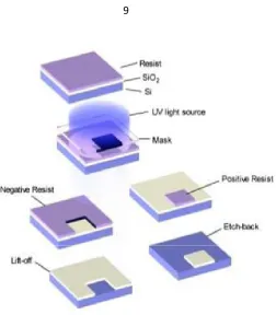
selectively removed by shining ultraviolet (UV) light on a specific area. Figure 1.5 shows the comparison of the fabrication process between positive and negative photoresist. A thin layer of
photoresist is first spin coated on the oxide layer. Then a photomask, consisting of a transparent glass
plate coated with an opaque chromium (Cr) pattern, is then placed in contact with the photoresist coated surface. The wafer is then exposed by the UV radiation in order to transfer the pattern on the
mask to the photoresist, which is then developed in the developer solution. The UV radiation induces the chemical reaction on the exposed areas of the photoresist. After the UV radiation step, the
positive photoresist is enhanced by UV radiation while the negative photoresist is weakened. In developing process, the developer removes either the exposed areas (positive photoresist) or the
unexposed areas (negative photoresist) of the photoresist. The pattern of photoresist-coated (positive
photoresist) or bare (negative photoresist) oxides is then left on the wafer surface. The resulting photoresist pattern is either the positive or negative image of the original master pattern of the
photomask. The chemical, such as hydrochloric acid, is applied to remove the uncovered oxide from the exposed areas of the photoresist. After that, hot sulphuric acid is used to remove the remaining
photoresist to complete the whole process. This chemical only removes the photoresist but not the
Figure 1.5. Comparison of the fabrication process between positive and negative photoresist. (Image courtesy of NCSU soft lithography from Wiki)
1.2.2 Bulk Micromachining
Bulk micromachining is the fabrication process applied to remove part of the bulk substrate. It is
a subtractive process used to create large pits, grooves and channels on the original substrate, as shown in Figure 1.6. Bulk micromachining can be performed by using wet etching with corrosive
etchants or a dry etching method such as reactive ion etching (RIE) or deep reactive ion etching (DRIE). Materials such as silicon and quartz are commonly used for wet etching, while silicon,
metals, plastics and ceramics are usually used for dry etching.
1.2.2.1 Wet Etching
Wet etching is usually applied in order to remove the materials on substrates by immersing in a chemical etchant liquid bath. These chemical etchants can be isotropic or anisotropic. Among them,
under the etching masks at the same rate as they etch through the material. This is the so called
"undercutting". The most common solution of the isotropic etchant for silicon is HNA, which consists of a mixture of hydrofluoric acid (HF), nitric acid (HNO3) and acetic acid (CH3COOH).
Isotropic etchants are limited by the geometry of the structure to be etched. Etch rates can slow down and in some cases they can stop by introduction of the diffusion limiting factors. However, this effect
can be minimized by agitation of the chemical etchant liquid bath, resulting in structures with near
perfectly rounded surfaces [18]. Anisotropic etchants, on the other hand, etch faster in a specific crystal direction. Potassium hydroxide (KOH) is the most common anisotropic etchant used in
process because it is comparatively safer. Besides, ethylene diamine pyrocatechol (EDP), tetra-methyl-ammonium-hydroxide (TMAH), and hydrazine water are the other common anisotropic
etchants used in MEMS process. Structures formed in the substrate by wet etching are dependent on
the crystal orientation of the silicon wafer substrate. Such anisotropic etchants etch faster in the crystal direction perpendicular to the (110) plane. However, they etch slower in the direction
perpendicular to the (100) plane. The direction perpendicular to the (111) plane is also etched very slowly. Silicon wafers, originally cut from a large ingot of silicon grown from single seed silicon, are
cut according to the crystallographic plane. They can be supplied in terms of the orientation of the surface plane. Dopant levels introduced in the substrate can affect the etching rate of KOH. They can
effectively stop the etching if the dopant levels are high enough. Boron is one of the typical dopants
which is commonly used in IC fabrication process. It is introduced into the silicon by the diffusion process. This can be used to selectively etch specific regions in the silicon, leaving doped areas
unaffected during wet etching process. By combining the anisotropic etching with etching stops, various silicon microstructures can be bulk micromachined.
Fig 1.6. Comparison of the bulk micromachining process: (a) Anisotropic etching. (b) Isotropic etching. (c) RIE.
(Image courtesy from terpconnect.umd.edu)
1.2.2.2 Dry Etching
Unlike wet etching with corrosive liquid or etchants, dry etching usually applies plasma-based reactive gases or vapors to perform the etching process, and it is usually at high temperatures.
Reactive ion etching (RIE), the most common form of dry etching method for MEMS process, utilizes the radio frequency (RF) power as the additional energy to drive the chemical reaction on the
targeted substrate to be etched. The physical bombardment by the energetic and reactive ions is
accelerated towards the targeted substrate to be etched within a plasma phase to supply the additional energy needed for the reaction. As a result, the etching can occur at much lower temperatures than
those usually needed at temperatures above 1000ºC. Besides, RIE is not limited by the crystal structures in the silicon structure. Therefore, deep trenches and pits, or even any shapes with vertical
walls, can be etched by RIE [18]. Deep Reactive Ion Etching (DRIE) is a much higher aspect-ratio etching process than RIE. In this technology, protective polymer is deposited and high-density
plasma etching is performed to achieve higher aspect ratios, as shown in Figure 1.7. The etching rates
Fig 1.7. Electrostatic comb-drive actuator fabricated by Deep Reactive Ion Etching (DRIE) of silicon-on-insulator (SOI) wafer.
(Image courtesy from www.actmost.eu)
The most noticeable difference in the fabrication process of MEMS from traditional integrated
circuit fabrication is the ability to modify the substrate with the two basic techniques: surface micromachining and bulk micromachining, as shown in Figure 1.8. Bulk micromachining features
[image:34.595.174.444.101.307.2]inside the substrate, while surface micromachining is based on the deposition and etching of different structure layers on top of the substrate. In the following, the detail will be introduced.
1.2.3 Surface Micromachining
Surface micromachining focus on the processing above the substrate, mainly using the substrate
as a foundation layer to build the other structures. Surface micromachining was originated in the 1980’s and is the contemporary MEMS fabrication technology. Because this process does not depend
on the etching characteristics of the substrate, various materials, such as soda lime, metals, and silicon on insulators (SOI) are also used in this process. Material is added to the substrate in the form
of thin film layers on the substrate surface by deposition or bonding. These layers can either be the
main structural layers or act as the spacers (sacrificial layers) for a suspended structure, which will be removed later by wet etching. Among them , common sacrificial materials include photoresist and
oxide. Hence the surface micromachining process usually consists of films with two different materials. One is the main structural material and the other is the sacrificial material. The sacrificial
material is first deposit on the substrate and patterned by dry etching process. Subsequently, these main structure layers are deposited on top of the sacrificial material and then dry etched to pattern the
microstructure. The sacrificial material is finally wet etched away to release the final microstructure.
Additionally, introduction of each additional layer will also result in higher difficulty in fabrication because of the increasing level of complexity. The process of a typical surface micromachined
cantilever beam is shown in Figure 1.9 (Left). Here, the oxide sacrificial layer is first deposited on the silicon substrate surface by photolithography process as the sacrificial layer. A polysilicon layer
is then deposited and patterned by RIE processes to form a cantilever beam with a pad anchored on
the silicon substrate. The wafer is then wet etched to remove the sacrificial oxide layer. The beam is finally released and left on the silicon substrate. Even more complicated MEMS structures, such as
Figure 1.9. (Left) Illustration of surface micromachining process. (Right) Polysilicon micromotor fabricated using a surface micromachining process.
(Image courtesy from www.mems-exchange.org)
Figure 1.9 (Right) shows another example: the polysilicon micromotor fabricated using a surface
micromachining process. In this device, five mechanical levels of micromachined polysilicon can be achieved using Sandia Ultra-Planar Multi-Level Technology (SUMMiT). The key point of the
surface micromachining process depends on the ability to successfully remove all of the sacrificial
layers to free the structural elements so that the micromotor can be actuated.
1.2.4 High-aspect-ratio Micromachining
High-aspect-ratio micromachining (HARM) is a process which utilizes micromachining to
fabricate structures followed by injection molding or embossing. Electroforming technique can also be applied to replicate microstructures in metals. HARM is one of the most popular technologies for
replicating microstructures because the nature of high-performance but low-cost. Commercial products fabricated by HARM include microfluidic structures, such as molded nozzle plates which
can be used for inkjet printing, and the microchannel plates in medical diagnostic applications.
Among them, the materials that can be used in HARM are the electroformable metals and plastics, such as polyimide, acrylate, and polycarbonate.
LIGA is an important fabrication process for high-aspect-ratio microstructures by tooling and
replication [19]. It exposes a thick acrylic resist of PMMA under a lithographic mask by applying X-ray synchrotron radiation, as shown in Figure 1.10. The exposed areas are then chemically dissolved.
Metals are subsequently electroformed in areas where the materials are removed. The tools insert for the succeeding molding step are then defined. LIGA has the capability of creating very well
fabricated microstructures up to 1000 μm high. However, LIGA usually has the limitation on the
need having access to an X-ray synchrotron facility.
Figure 1.10. LIGA process: (a) Exposure. (b) Electroplating. (c) Finishing to height. (d) Removal of the substrate.
(Image courtesy from www.micro-works.de)
1.2.4.2 Laser Micromachining
Laser micromachining processes usually are not fast enough for effective MEMS fabrication process because the unparallel nature. However, they are still useful in some micromachining areas,
such as making a mold. For example, excimer laser micromachining technique is applied particularly
for the micromachining on plastics and polymers because those materials cannot removed by traditional processes like burning or vaporization. Besides, materials adjacent to the laser area are not
found some other applications in MEMS area. Among them, laser cutting, laser drilling, laser
annealing, and etching are the most common applications.
1.3 Parylene
Parylene is the trade name for members of a unique family of plastic polymers which are
deposited by the dimer of para-xylylene (di-para-xylylene, or DPXN) [21]. It was first discovered by Dr. Michael Mojzesz Szwarc at the University of Manchester, England, in 1947 and commercialized
by Union Carbide Corporation in 1965 [22]. Parylene is used in various industries because of its many excellent properties. Among them, the major application is in the electronics industry for the
application on the printed circuit board (PCB) coating. Here, parylene protects the electronic devices against damages from moisture and corrosive etchants. Figure 1.11 shows the chemical structures of
the three most commonly used parylene types: parylene-N, parylene-C, and parylene-D. A new
parylene variant, which is called parylene-HT is also demonstrated here. In which, parylene-N is poly-para-xylylene, a completely linear and highly crystalline polymer; parylene-C is essentially
parylene-N with a chlorine atom replacing one of the aromatic hydrogens; parylene-D is very similar to parylene-C, but with two aromatic hydrogens being replaced with chlorine atoms. The benzene
backbone of the parylene family makes them very chemically inert. At the same time, the
Figure 1.11. Chemical structure of Parylene-N, -C, -D, and-HT and the process temperature.
A list of selected properties of parylene-N, -C, -D and -HT is shown in Table 1.1. Parylene
exhibits outstanding mechanical strength and flexibility as a thin film coating. With Young’s modulus of around 4 GPa (similar to Nylon) and an elongation-to-break percentage of more than
200%, parylene-C is a perfect membrane material on bio-MEMS applications.
Besides, parylene is also an excellent electrical insulator with high electrical resistivity. For
example, the breakdown voltage for 1 μm thick parylene is over 200 volts. Because the parylene film
is highly conformal and pinhole free, it is also an excellent barrier to gas and moisture with moderate thickness. In addition, parylene is extremely inert to many chemicals and solvents. Based on the
manufacturer’s study, solvents have a minor swelling effect on parylene-N, -C, and -D, with a 3% maximum increase in film thickness. The swelling is found to be completely reversible after the
solvents are removed by vacuum drying. Inorganic reagents, except for oxidizing agents at elevated temperatures, have little effect on parylene. Optically, parylene is transparent in the visible light
range. It only absorbs light under 280 nm in wavelength, which unfortunately limits its UV
applications. Due to their slightly different chemical structures, the four types of parylene also differ in properties. Parylene-N has very good gap penetration characteristics. However, parylene-N also
has the slowest deposition rate. Parylene-D can withstand higher temperature than parylene-C. Parylene-C has a useful combination of electrical and physical properties, plus a very low
faster than that of the other two. Parylene-C is hence the better choice for most traditional biomedical
applications. Parylene-HT is the new variant, and is expected to be a good prospect with its better thermal stability, improved electrical properties, increased UV stability, better crevice penetration,
lower coefficient of friction, and better barrier properties [23]; it is also ISO 10993 biocompatible [24-26].
The parylene deposition process, called Gorham process [27], and the involved chemical
processes are illustrated in Figure 1.12. The process starts with placing parylene dimer (di-para-xylylene), a stable compound in granular form, into the vaporizer, and the substrate to be coated into
the deposition chamber. The whole system is pumped down to medium vacuum. The dimer is then heated in the vaporizer and sublimes into vapor at around 180 °C. The dimer vapor enters the
pyrolysis furnace, controled at 690 °C, where the parylene dimers are dissembled into identical
monomers (para-xylylene). In the room-temperature deposition chamber, the monomers reunite on all exposed surfaces in the form of polymers (poly-(para-xylylene)). The deposition takes place at the
molecular level. The monomers are extremely active molecules which have a mean free path on the order of 1 mm (under deposition pressure of around 100 mTorr), resulting in superior penetration
ability and a high degree of conformability to the exposed surfaces. Also, the coated substrate temperature never increases more than a few degrees beyond ambient temperature. Additional
components of the parylene coating system include a mechanical vacuum pump and associated cold
trap for pressure control. The process of parylene-C is almost identical to all four types of parylene, except for some minor differences in the setting of pyrolysis temperature and deposition pressure.
Typical deposition thickness ranges from five to tens of microns. It can also be deposited as thin as hundreds of angstroms as a semi-permeable structure for the application on filters. The deposition
thickness can be controlled by the amount of dimer placed in the vaporizer. The normal deposition rate of parylene- C is about 3 μm per hour. It is directly proportional to the square of the monomer
rates can result in films with poor quality, which often appears as a opaque milky film, in contrast to
[image:41.595.29.564.439.717.2]the normal clear transparent ones.
Figure 1.12. Illustration of the deposition system of Parylene and the process flow.
Table 1.1 Important properties of Parylene-N, -C, -D, -HT, and PDMS [28-29].
Property Parylene N Parylene C Parylene D Parylene HT PDMS [29]
Dielectric Strength (V/mil), 1 mil film 7,000 5,600 5,500 5,400 610 [75] (1 mm film)
Dielectric Constant 60 Hz 1 kHz 1 MHz 2.65 2.65 2.65 3.15 3.10 2.95 2.84 2.82 2.80 2.21 2.20 2.17 2.3-2.8
Young’s Modulus (psi) 350,000 400,000 380,000 -- 52 – 126
Index of Refraction 1.661 1.639 1.669 -- 1.4
Yield Strength (psi) 6,100 8,000 9,000 -- 325
Elongation to Break (%) 20-250 200 10 -- 210 – 310 [30]
Coefficient of Friction Static Dynamic 0.25 0.25 0.29 0.29 0.33 0.31 0.145 0.130 -- 0.43-0.51 [31]
Density (g/cm3) 1.10-1.12 1.289 1.418 -- 9.7*10-4
Melting Point (°C) 420 290 380 >450 -49.9 – 40
Thermal Conductivity at 25 °C (10-4 cal/(cm*s*°C))
Water Absorption (% after 24 hours) < 0.1 < 0.06 < 0.1 < 0.01 -- (depends on cure conditions)
Specific Heat at 20 °C (cal/g*°C) 0.20 0.17 -- -- 0.35
1.4 Integration Technology
1.4.1 Traditional Chip Integration Technology
Soldering
Soldering, as shown in Figure 1.13, is a bonding process used to connect two separate metals together with a third metal which usually has a much lower melting temperature compared to the
other two metals that need to be connected together. In addition to the physical reaction, there is also a chemical reaction happened in the soldering bonding process. Soldering bonding process is mainly
applied to create a convenient and fast joint to make a good electrical contact between two separate metals. Solders typically do not provide very high mechanical strength because of the soft nature of
popular solder materials. Soldering process is used extensively in the electronics industry for discrete
components connected with printed circuit boards (PCBs). Its advantage is the easy application for quick and dirty bonding of discrete components with PCBs for bench testing, but the physical
weakness of the solder bonding, toxicity of the materials, local heat problem necessary for bonding, and its inability to connect small and dense array pads makes soldering a less attractive choice than
Figure 1.13. Demonstration of soldering. (Image courtesy from letsmakerobots.com)
Wire Bonding
Wire bonding, as shown in Figure 1.14, is a process used to connect an on-chip pad and a substrate pad with a fine conducting wire. This substrate may be another chip or the bonding pads on
PCBs. Popular materials for wire bonding include gold (Au) and aluminum (Al). The main advantage of wire bonding technology is the low-cost characteristics. However, the disadvantages include the
requirements of larger bonding pads with size of around 100 × 100 µm2, and larger bonding pitch
with size of around 200 µm. Besides, wire bonding requires large quantities of gold. It also has lower production rate, relatively poor electrical performance, and variations in bonding geometry. The
robustness and reliability are also serious issues. In addition, it cannot be used on flexible PCBs for implant application since the wire bonder can easily damage the flexible substrates.
To date, the most advanced wire bonders can achieve up to around 14 wires per second.
addition, the wire bonding technology is extremely flexible: changes in die size can be
[image:44.595.153.464.181.429.2]accommodated without noticeable additional costs.
Figure 1.14. Demonstration of wire bonding. (Image courtesy from www.caltexsci.com)
Flip Chip
Flip chip bonding technique, as shown in Figure 1.15, is developed to make electrical connection
between the face-down components onto substrates, carriers, and PCBs by solder bumps on the chip
bonding pads. Since wire bonding, the older technology which is gradually replaced by flip chip, uses face-up chips with a fine wire connection to each pad, therefore, the huge impedance
contributed by the fine and long wire might be an issue. However, in flip chip, the interconnect length between the chip and the substrate is much shorter, and thus the impedance of interconnect is
well controlled to be smaller. This is part of the reason that flip chip is applied in high clock speed
connecting all I/Os in a single process step. Besides, the solder bumps can be placed over the whole
chip surface, which implies the ability to make connections to the chip with significantly higher I/O density. This advantage allows additional power and ground connection, which is possible to further
increase the electrical performance.
While the flip chip bonding technique benefits the devices with high performance, its high cost is
still the main challenge and limitation for main stream applications. Thus, much effort and attention
continues to be made to reduce the costs. Besides, the toxic joint materials, solder bumps, are totally not desirable for implantable devices. Additionally, the global heating needed during bonding
process also limits its application on some substrates which cannot stand at high temperatures.
Figure 1.15. Demonstration of the process of flip chip assembly. (Image courtesy from www.chipscalereview.com)
1.4.2 State-of-the-art Chip Integration Technology
1.4.2.1 Microflex
Microflex (MFI) is a new three-dimensional (3D) interconnect technique developed by the
Fraunhofer Institute for Biomedical Engineering in Germany. Meyer et al. [32] utilizes a polyimide based multiple strand flexible ribbon cable with a photolithography patterned double metallization
correspond to the bonding pads on the chip. The via-hole of the contact pads on the ribbon cable is
then filled with metal balls or wedges applied by a commercial wire bonder. The metal pair is welded and results in a mechanically stable and electrically reliable contact. This technology, though derived
from the common wire bonding technology, is specifically designed and developed to integrate the passive and active electronic components to the electrodes, as shown in Figure 1.16.
The applied materials, such as polyimide substrate, platinum, and irridium, in this technology
showed an excellent biocompatibility during in vitro and in vivo testing. In addition, this substrate has also proved to be non-cytotoxic according to the international standard DIN EN ISO 10993. Also,
in chronic implantations in the sciatic nerve of rats and on the retina of rabbits, they caused no significant tissue reactions or alterations. The Microflex technology can also be applied to
three-dimensional (3D) structures and the density is comparable to that of the flip chip technology. Several
ultrasound array sensors, retinal stimulators (EPIRET), and multiplexer modules have been integrated successfully with this technology [32–35].
The current device, EPIRET 3, has transmitting coils on external glasses and an internal receiver coil and chip secured in the eye in place of the lens, as shown in Figure 1.17. It can transfer energy
and data from the external power source to the implant. Based on the design of epiretinal prosthesis, the stimulator was placed slightly inferior to the fovea and fixed with retinal tacks. In an exploratory
human trial in 2009, the device was implanted for four weeks to observe the safety of the device and
how well it would work. There was mild inflammatory response in some of the six patients which were treatable by local antibiotic and steroids, but they decided there was no lasting damage from the
prosthesis. Four of the six patients gained light perception, one gained hand movement, and one had no light perception [36]. However, more clinical trials are still needed to demonstrate the long-term
biocompatibility. Besides, the mechanical properties of the bond on the substrate have yet to be tested as well. In addition, its tedious and low yield process also makes it difficult and costly to
Figure 1.16. (Left) Overview of the Microflex technique. (Right) SEM pictures of the contact array. [34]
Figure 1.17. Final implant with parylene C and silicone rubber encapsulation [35].
1.4.2.2 Boston Retinal Implant Project
Dr. Wyatt and Dr. Rizzo from Massachusetts Institute of Technology developed a subretinal
implant device aiming to achieve the goal of visual prosthesis [37]. This device is also based on the polyimide substrate. The host flexible circuit was made by defining the metal trace with width of 50
prosthesis components were then assembled on the host polyimide substrate. Because the period for
the animal surgical implantation trials was limited, these traces were fabricated from a Cu/Ni/Au metallization which were commonly used in industry for microelectronics. Besides, the coils were
fabricated from Cu wire. Standard surface-mounted components were used for all the off-chip power supply parts, and these were assembled on the flex circuit substrate using conventional wave
soldering techniques. The ASICs were mounted by stud bumping with 75-µm-high Au bumps,
followed by flip-chip die attachment to the host substrate. The stud bumping was also used for the flex-to-flex connections between the flex circuits and the electrode arrays.
Although this device has gone through several in vivo studies, the integration approach proved to be prone to reliability problems. Also, the encapsulation coating by PDMS has less reliable
Figure 1.18. Schematic representation of the minimally invasive ab-externo approach. The transmitter coils are placed outside on a pair of eyeglasses and the receiver coils and the stimulator
chip are placed on the eyeball. The electrode array is placed in the subretinal space through a scleral flap [37].
1.4.2.3 California Institute of Technology—CL-I2
Rodger and Li et al., have developed a chip level integrated interconnect (CL-I2) and further extended to an embedded chip integration technology and successfully demonstrated by integrating
the flexible polymer (parylene) substrate RF coil with commercially available IC chips and other passive discrete components [38-39]. Figure 1.19 illustrates the conceptual schematic of this
carrier silicon wafer and directly integrated with an MEA and with, ultimately RF coil power and
data connections. Finally, all the components will be further sealed with a parylene coating.
The cavity matching the chip dimension is first etched on the parylene-on-silicon substrate for
chip placement by DRIE. After the chip is dropped into the cavity, parylene deposition is performed again to seal the chip and serve as the insulation between two metal layers. Then, the metal is
deposited and a photolithography step is done to make the electrical connection between the pads on
the chip and the other pads on outside components. The structure is finally released by back etching of the silicon substrate.
The parylene substrate to be integrated with the chip is based on the parylene-based skin technology which has been well characterized both in vitro and in vivo and is also approved by the
FDA for long-term human implantations. However, the alignment problem that arises during the
“chip-drop” could severely affect the feasibility of this technology. The surface flatness inside the cavity will limit the metal connectivity over a step. Furthermore, the low alignment efficiency of the
bonding pads on the chip with the metal bonding pads embedded in the parylene skin renders the integration inefficient.
Figure 1.19. (Left) Illustration of the CL-I2 packaging concept [38]. (Right) Concept of embedded
1.5 Layout of the Dissertation
Chapter 2 first introduces the overview of the requirements for device packaging, and two generations of parylene flex fabrication. It also describes the integration technology for high-density
multi-channel retinal IC chips. Other technologies related to the integration are also discussed.
Besides, details on how to build a parylene flex with reliable metals and strong adhesion are also addressed. Chapter 3 demonstrates the application of photo-patternable adhesives on chip integration
technology. The setup is built and the bonding force is measured. Functionalities of two real retinal IC chips are also successfully tested via the parylene flex to further confirm the effectiveness.
Chapter 4 focuses on the lifetime study and surgical mockup design. The long-term packaging reliability is proved by accelerated and active lifetime soaking test. In addition, the mockups for
512-channel and 1024-512-channel retinal IC chips are both successfully implanted in a dog's and pig's eye.
Chapter 5 presents the final wireless 1024-channel retinal implant device. A parylene flex with a dual-metal-layer structure is first successfully built to relax the metal interconnections. Treatments on
stimulating output electrodes are also studied. Complete integration of the 1024-channel retinal IC chip, discrete components, and coils with parylene flex is also introduced here.
1.6 Summary
This chapter introduced the mechanism of the retinal prosthesis and the two most common
leading causes of blindness induced by degenerative retina: age-related macular degeneration (AMD) and retinitis pigmentosa (RP). MEMS technologies, including photolithography, bulk, surface,
high-aspect-ratio, and laser micromachining, that are used to build the all parylene flex in this thesis were
and flip chips, and state-of-the art chip integration technology with a bio-device were also discussed
in order to compare the pros and cons. A reliable high-density packaging scheme that allows stimulating circuitries to be integrated with the bio-device is definitely in high demand, but current
state-of-the-art technologies still lack the ability to demonstrate high-density multi-channel connection to commercial IC chips. Parylene-family with high biocompatibility which is compatible
with MEMS technology is believed to be one of the best materials on the implant application.
Therefore, a flexible parylene flex combined with integration technologies which will be discussed in the following chapters will be used to address the issues and to achieve full system integration.
1.7 Reference
[1] The Eye Diseases Prevalence Research Group, "Prevalence of age-related macular degeneration in the United States," Archives of Ophthalmology, vol. 122 (4), pp. 564-572, Apr 1, 2004.
[2] G. Fishman, V. Vasquez, M. Fishman, and D. Berger, "Visual loss and foveal lesions in Usher's syndrome," British Journal of Ophthalmolology, vol. 63 (7), pp. 484-488, Jul 1, 1979.
[3] E. W. D. Norton, M. F. Marmor, D. D. Clowes, J. W. Gamel, C. C. Barr, A. R. Fielder, J. Marshall, E. L. Berson, B. Rosner, M. A. Sandberg, K. C. Hayes, B. W. Nicholson, C. Weigel-DiFranco, W. Willett, J. S. Felix, and A. M. Laties, "A randomized trial of vitamin A and vitamin E supplementation for retinitis pigmentosa," Arch. Ophthalmol., vol. 11, pp. 1460-1466, 1993. [4] J. Bennett, T. Tanabe, D. Sun, Y. Zeng, H. Kjeldbye, P. Gouras, and A. M. Maguire,
"Photoreceptor cell rescue in retinal degeneration (rd) mice by in vivo dene therapy," Nature Medicine, vol. 2, pp. 649-654, 1996.
[5] M. Humayun, R. Propst, E. de Juan, Jr., K. McCormick, and D. Hickingbotham, "Bipolar surface electrical stimulation of the vertebrate retina," Archives of Ophthalmology, vol. 112 (1), pp. 110-116, Jan 1, 1994.
[6] E. Zrenner, A. Stett, S. Weiss, R. B. Aramant, E. Guenther, K. Kohler, K.-D. Miliczek, M. J. Seiler, and H. Haemmerle, "Can subretinal microphotodiodes successfully replace degenerated photoreceptors?" Vision Research, vol. 39, pp. 2555-2567, 1999.
[8] S. Y. Kim, S. Sadda, J. Pearlman, M. S. Humayun, E. D. Jr., and W. R. Green, "Morphometric analysis of the macula in eyes with disciform age-realted macular degeneration," The Association for Research in Vision and Ophthalmology annual meeting, vol. 42, 2001.
[9] A. Y. Chow, V. Y. Chow, K. H. Packo, J. S. Pollack, G. A. Peyman, and R. Schuchard, "The artificial silicon retinamicrochip for the treatment of vision loss from retinitis pigmentosa," Arch. Ophthalmol., vol. 122, pp. 460-469, 2006.
[10] A. Y. Chow and V. Y. Chow, "Subretinal electrical stimulation of the rabbit retina," Neuroscience Letters, vol. 225 (1), pp. 13-16, Mar 28, 1997.
[11] M. S. Humayun, J. D. Weiland, G. Y. Fujii, R. Greenberg, R. Williamson, J. Little, B. Mech, V. Cimmarusti, G. Van Boemel, and G. Dagnelie, "Visual perception in a blind subject with a chronic microelectronic retinal prosthesis," Vision Research, vol. 43 (24), pp. 2573-2581, Nov., 2003.
[12] M. S. Humayun, R. Freda, I. Fine, A. Roy, G. Fujii, R. J. Greenberg, J. Little, B. Mech, J. D. Weiland, and E. de Juan, "Implanted intraocular retinal prosthesis in six blind subjects," Investigative Ophthalmology and Visual Science, vol. 46, pp. 1144, 2005.
[13] J. D. Weiland, W. Liu, and M. S. Humayun, "Retinal prosthesis," Annual Review of Biomedical Engineering, vol. 7 (1), pp. 361-401, 2005
[14] Berkeley Sensor and Actuator Center, http://bsac.eecs.berkeley.edu
[15] Sandia National Laboratories, SUMMiT * Technologies, http://www.mems.sandia.gov [16] University of Stanford, http://www.stanford.edu/group/SML/ee321/ho/MEMS-01-intro.pdf [17] Petersen, K.E., Silicon as a Mechanical Material, Proceedings of the IEEE, Vol. 70, No. 5,
pp.420-457, May, 1982.
[18] Kovacs, G.T.A., Micromachined Transducers Sourcebook, McGraw-Hill, New York, NY, 1998.
[19] Defense Advanced Research Projects Agency (DARPA), http://www.darpa.mil/MTO/
[20] Bryzek, J., Peterson, K., and McCulley, W., Micromachines on the March, IEEE Spectrum, pp. 20-31, 1994.
[21] M. Gazicki, G. Surendran, W. James, and H. Yasuda, "Polymerization of Para-Xylyene Derivatives (Parylene Polymerization). II. Heat Effects during Deposition of Parylene C at Different Temperatures," Journal of P

![Figure 1.2. System overview and comparison of locations of epiretinal and subretinal implants [13]](https://thumb-us.123doks.com/thumbv2/123dok_us/955452.608738/25.595.122.494.284.553/figure-overview-comparison-locations-epiretinal-subretinal-implants.webp)
![Figure 1.4. Complexity of MEMS device by structure layers [15].](https://thumb-us.123doks.com/thumbv2/123dok_us/955452.608738/27.595.90.531.396.600/figure-complexity-mems-device-structure-layers.webp)