Power-Control Strategy of a Current Source Converter for
High-Power Induction Melting
Muhammad Nawaz1* and Muhammad Asghar Saqib2
1. Department of Electrical Engineering, University of Engineering and Technology, Lahore 54890 (Pakistan)
2. Department of Electrical Engineering, University of Engineering and Technology, Lahore 54890 (Pakistan)
* Corresponding Author: E-mail: [email protected]
Abstract
This paper presents a power control scheme of a current source converter (CSC) which delivers a constant current to the load for induction melting applications. The proposed control scheme with SVPWM pattern regulates the power of a high Q- resonant load by controlling the DC current according to the defined target. The PI controller adjusts the manipulated variable by SVPWM in such a way that the error signal is reduced to a minimum value and a constant current is maintained uninterruptedly for the load. In order to validate this constant current requirement to the load, the output power analysis of the resonant inverter is also carried out in this work. The proposed control scheme is described through simulation in Matlab and the results show its effectiveness in induction-melting applications.
Key Words
: PI-Controller; Space-vector pulse width modulation (SVPWM); Current source converter (CSC); Resonant inverter; Quality factor; Induction heating.1. Introduction
Induction melting is a type of heat-treatment process that works on the principle of electromagnetic induction. The induction heat treatments such as melting, tempering, forging and brazing etc. have evolved very rapidly grown in recent years [1]-[4]. The reason of this wide-spread use of induction heating compared to other heating practices is due to its rapid response, and clean and efficient way of heating [5]-[8].
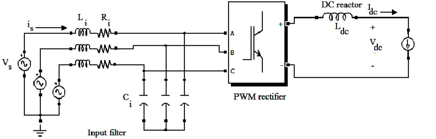
A topology for induction melting can be built up with the help of a current-source converter followed by a DC reactor which aids to feed a smooth current to the load as shown in Figure 1. This constant current is then supplied to a resonant inverter for energizing the resonant tank. The resonant tank itself comprises a parallel combination of capacitor and inductor’s coil, produce a self-oscillating behaviour in the circuit when is energized. This oscillating behaviour is called ‘resonant frequency’ and is used in induction melting.
Various strategies, for the control of power of resonant inverters have been established [2], [4], [5], and [9]. A brief overview of the previous work is given in the following paragraphs.
Ngoc et al. in reference [2], presented a technique for the control of coil-current amplitude and phase angle to regulate the output power. The buck converter at the rectifier output adjusted the inverter’ input voltage and, in turn, the output power through converter’ duty cycle regulation generated by the amplitude controller. In reference [4], the authors used a PWM control scheme to regulate the buck converter connected at the rectifier output. The buck converter was employed for the variation of output voltage to control the load power through a PLL scheme. Fuentes et al. developed an induction furnace which consisted of a controlled rectifier followed by a boost converter to feed the inverter bridge: the scheme was employed to control the output power through DC voltage regulation [9].
References [2], [4] and [9] have proposed topologies for resonant inverters comprising of a front end rectifier with buck or boost converters for power regulation. These added switching devices (i.e. buck and boost converters) enhance the system size, cost and create control complications when linked with a conventional firing angle controlled rectifier.
In reference [5], Chudjuarjeen et al. have addressed a current-fed inverter for forging applications. In this work, the PI control strategy has been used to generate firing pulses for the SCR-bridge rectifier. Conventionally this method is known as firing angle control scheme. The DC current from rectifier output and high frequency voltage from resonant tank capacitor are sensed and used by this scheme for power adjustment. One flaw of this strategy is the utilization of high-frequency resonant-tank voltage for control purpose so another converter is needed to convert this voltage into DC. This extra converter enhances the costs, losses and size of a system. Hence, a well-controlled system having minimum components, with optimum switching states modulation scheme, is needed to avoid these extra devices and control components.
The presented work, in this paper, proposes a quite simple and active control scheme with reduced control components. A vital factor for the design and
analysis of a proposed system is the availability of an extensive choice of design tools in both software and hardware. One best opportunity to design and simulate a system with bit and cycle accuracy is MATLAB Simulink which offers a good picture of system response [10], hence is used in presented work for the development of the proposed model.
In this model, the control strategy measures the DC current and then compares it to the reference signal. The difference signal is fed to the PI controller which adjusts the manipulated variable by SVPWM in such a way that the error signal may approach to zero and a constant current is maintained continuously for the load. The key objective of this constant current is to avoid the fluctuation of the output power as load varies in heating process. The power analysis at the output of the current fed inverter is also carried out in order to validate the effectiveness of the control scheme in melting applications.
2. Proposed Control Architecture with
Space Vector-PWM Pattern
2.1 Control scheme
PI controllers can give a better response and removes the control error when desired target is cnstant (i.e. DC value) in steady state. Hence, in this represented model, a PI controller is an effective solution with satisfactory outcomes. It can be expressed as:
ti
t e d
T t e k u
0 ( )
1 )
( (1)
Where,
e
(t)
r(t)
y(t)
, y(t) is the output DC current Idc and r(t) is the reference signal.The control strategy is shown in Figure 2 where DC current signal is compared with the reference signal and their difference gives an error signal. The error signal is then fed to the PI controller. The PI controller with SVPWM generates the gate drive pulses for rectifier and produces such a value of manipulated variable that the output current may track the reference value accurately. As in current source converter, a DC current is desired to feed the load circuit, so the control scheme supplies the DC current to the load.
Fig. 2: Proposed control scheme with SVPWM. The power control of the converter is realized through the DC current adjustment, hence a rated controlled power i.e.
P
V
dc
dc can be achieved at the rectifier output.2.2 Space vector PWM
Space vector-PWM is an advanced digital modulation scheme which works with vector-time averaging approach and generates desired pulses for converter’s switches [11], [12], [13], [14] and [15]. SVPWM modulation has some dominant features over other modulation techniques such as optimized state selection, lower harmonics and easy implementation through a microprocessor [16]; hence is selected for study in this research.
Space vector pulse width modulation is frequently used both for voltage source and current source topology. For current source converter, there is a slight modification of the conventional SVPWM used in voltage source configuration. Like a voltage source converter, there are six active vectors in current source converter, but three zero vectors are formed to freewheel the DC current through the bridge. In the voltage source topology, at any instant three phases are utilized by the space vector PWM, whereas in current source topology only two phases are used [12], [13], and [15].
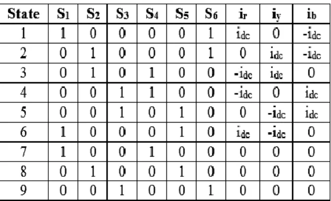
During this current source operation, one switch in the upper legs (S1, S2, and S3) and one switch in the
lower legs (S4, S5, and S6) of the converter must be
switched-on at any instant of time to ensure source connection to the load and obey:
1
3 2 1S S
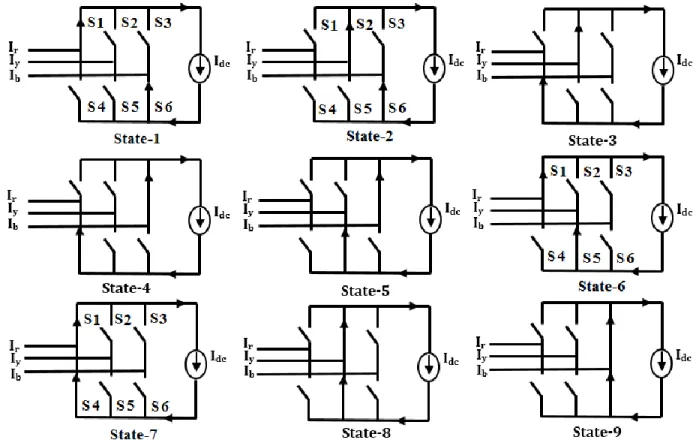
S and S4S5S61 (2) These constraints give nine possible switching states for the current source configuration as shown
in Table 1. Based on this possible on/off combination of the power devices, the switching states diagram of the CSC can be drawn as shown in Figure 3.
Table 1: Switching States
One could notice that at any instant no two switches of upper or lower leg of the converter can never be ‘ON’ to avoid the short circuiting of input phases.
The line current can be written in a balanced three phase system as:
) (cos
I t
ir p (3)
) 3 2 (cos
I t
iy p (4)
) 3 2 (cos
I t
ib p (5)
Current space vector is then defined as:
I jI
Isv (6)
Where;
ir iy ib I
2 1 2 1 3 2
(7)
iy ib I
2 3 2
3 3 2
(8)
The converter states with respective line currents given in Table 1 can be used in equations (5), (6) and (7) to express the αβ- components, which produce possible current vectors as follows:
6
3 2 1
j dce
I
6 3 j dc
2 I e
3 2 I
(10)
The remaining current vectors I3,I4,I5 and I6 can be found in the same way. The zero current vectors are I7 I8 I90.
These current vectors can be described in a general expression as follows:
9 , 8 , 7 i 0
6 , 5 , 4 , 3 , 2 , 1 i e
I 3 2 I
6
) 1 i 2 ( j dc
i (11)
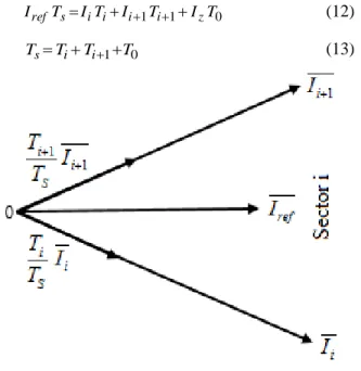
Six active vectors generates hexagon in αβ-reference frame. This hexagon can be divided into six sectors, as shown in Figure.
The on time of vectors can be calculated in each sector. From the Figure 4, assuming Iref is lying in a
sector ‘i’, the adjacent active vectors Ii, Ii+1, and zero
vector Iz with their respective on times Ti , Ti+1 and
T0, are used to evaluate the reference current vector.
Fig. 4: Switched vectors and sectors for CSC. Fig. 3: The switching states diagram of the CSC.
0 1
1T I T
I T I T
Iref s i i i i z (12)
0
1 T
T T
Ts i i (13)
Fig. 5: Reference vector Iref in sector i.
A general relation for the desired vector on times can be established by using equation (10), (11) and (12) as follows [12]:
1 5 0 _ _ 6 6 6 6
1 sin(2 3) cos(2 3)
) 1 2 ( cos ) 1 2 sin( i i ref ref dc s i i T T T T I I i i i i I T T T (4)
where, Iα_ref and Iβ_ref are the horizontal and vertical
components of the reference current vector Iref.
3. Model Configuration
The structure of the system mainly consists of a front end controlled rectifier, dc reactor, inverter bridge and parallel resonant tank at the output. Conventionally, an SCR based rectifier is used for the AC-DC conversion due to its low cost but it deteriorates the system power quality significantly. The recent trend, to meet the criteria of power quality, is to replace the SCR based rectifier with a PWM converter so an IGBT based rectifier bridge is used in this study as shown in Figure 1[17]. The SV-PWM switching pattern has been used with proposed control scheme to supply a constant current to the inverter bridge.
The inverter bridge is followed by the combination of a capacitor and coil configured in parallel commonly known as tank circuit as shown in Figure 6 [18]. This tank circuit forms a ‘resonant
frequency’ when is energized. This ‘resonant
frequency’ can be expressed as:
LC fr 2 1 (15)
The resonant capacitor and coil are fixed in this combination; however, the load parameters i.e. conductivity, permeability and geometry tend to change during the heat treatment process resulting in the change in equivalent load and fluctuation in power. The system parameters are also given in Table 2.
Fig. 6 Current source feeding resonant tank. Table 1 System Parameters
Input voltage (3-phase) 380 V
Frequency
50 Hz
Input filter inductance 6.05µH
Input resistance 20 mΩ
Input capacitance 50 µF
DC smoothing reactor 25 mH DC load resistance 0.8 Ω PI controller gain term 1.3 PI controller integral term 56
Coil inductance 452 µH
Equivalent load resistance 0.02 Ω Capacitance bank 8.95 µH Switching frequency 10 kHz
Modulation index 0.93
Resonant frequency 2.5 kHz
Sample time 2e-6 s
4. Power Analysis
As the purpose of the proposed control strategy is to supply a constant current to the load, hence in this section the output power of the parallel resonant load is also presented to examine the usefulness of the proposed control scheme.
Conventionally in the induction heating or melting, the load circuit has a small resistance which is characterized by its quality factor. The quality factor of a resonant circuit illustrates the maximum energy stored to the energy dissipated in a circuit during one oscillation period. It is a dimensionless quantity and lies in the range 5-20 [19]. Mathematically, it can be represented as:
r L
Qf (16)
where ‘L’ is inductance, ‘r’ is resistance and ‘
’ is oscillation period. Selection of these parameters gives a value of quality factor and in this presented work its value is 7.03 that exists in acceptable range.The quality factor is considered a key parameter in the induction heating and is very helpful to examine the electrical quantities i.e. Voltage, current and power etc.
The output voltage, active and reactive component of the voltage can be related using Q- factor as: 2 , , 1 f peak o peak r Q V V (17) peak r f peak
L Q V
V , , (18)
Then, the output power can be found as follows:
R V Po r peak
2 2 , (19) R Q V P f peak o o ) 1 .( 2 2 2 , (20)
Similarly, the current flowing through the coil or load can also be used to find the output power as:
r R i Po L peak.
2 2
,
(21)
The inverter instantaneous current, voltage and power can be represented in the following relation [20]:
1 ) ( sin k invinv i k t
i (22)
1 ) ( sin k oo v k t
v (23)
1 ) ( sin k invinv i k t
i
) .cos (sin 1
k
o k t
v (24)
Conversely, inverter input side power i.e. DC power can be measured easily and in industry, it is considered approximately equal to the output power by ignoring electrical and thermal losses. The reason of this approximation is easy measuring and control of the DC parameters. This DC power is represented with this simple relation:
dc dc dc V I
P (25)
5. Results and Discussion
The development of the proposed work is achieved thanks to the availability of electric power system design tools such as MATLAB Simulink. MATLAB Simulink was opted due to its bit and cycle accuracy to perform the simulation of the system; the results of which are shown in Figs. 7–11.
Figure 7 shows the DC voltage (
V
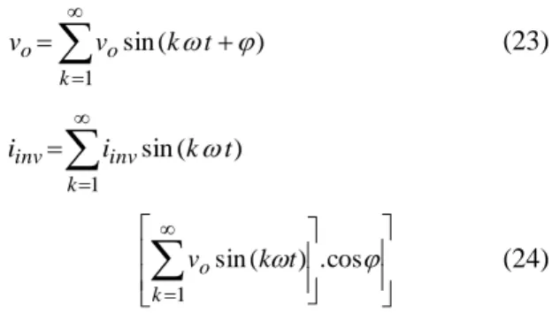
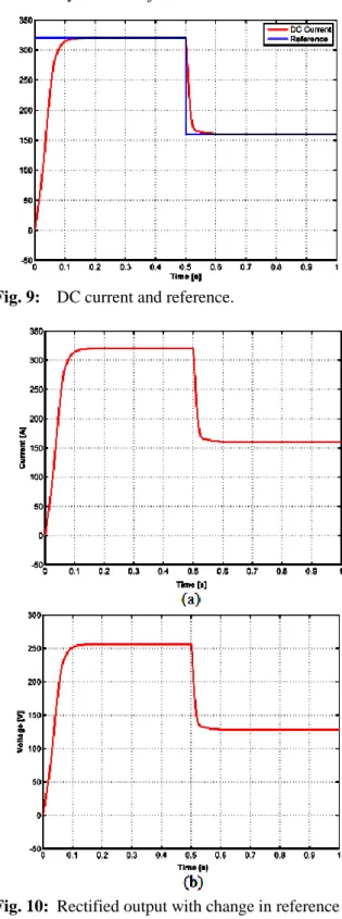
dc) and current (Idc) at the rectifier output. The DC current was set at 320 A that reaches its steady state value within a short time and the respective rectified DC voltage i.e. 256 V also attains steady state value; hence, power can be obtained simply by the multiplication of the voltage and current. At this reference, three phase line current and voltage are shown in Figure 8.Figure 9 shows the reference current and the actual current: this illustrates the effectiveness of the control scheme for the target’ tracking.
Similarly, it can be seen clearly in Figure 10, with the change in reference value of the DC current, respective DC voltage is altered, hence power i.e.
dc dc dc V I
P is also changed. Therefore, this figure demonstrates power control based on DC current setting through a reference value.
Fig. 7: Rectifier output (a) DC current and (b) DC voltage.
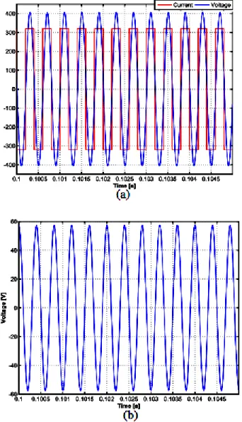
Fig. 8: At constant reference: Three phase line (a) current and (b) voltage.
At begin t- 0 sec, reference current was set at 320 Amp, then at 0.5 sec, it was reduced to 50 % i.e. 160 A. one could notice that power control is achieved by current adjustment.
Fig. 9: DC current and reference.
Fig. 10: Rectified output with change in reference (a) DC current and (b) DC voltage.
Figure 11 illustrates the output quantities of the inverter which are helpful for the validation of parameters analysis given in equations (16) - (20). In the analysis, peak values are considered due to the simulation work, however, in a practical system effective values of these quantities are preferred. In Figure 11 (a) the square waveform represents the current flowing through the inverter and sinusoidal waveform expresses the output voltage which is 405 V. In Figure 11 (b) & (c) voltage across active and reactive components can be seen as 57 V and 401 V respectively. Putting respective quantities in equations (16) and (17) same results are found as in figures. Similarly, looking at Figure (d), inductor current has been seen 2855 A. The output power i.e. 81kW can be determined by using the power relations presented in equations (18), (19) and (20).
Fig. 11: Current fed resonant inverter (a) output voltage and current, (b) active component of output voltage (c) reactive component of output voltage (d) resonant current flowing through the coil or load.
6. Conclusion
A power-control strategy with space vector pulse width modulation of current source converter has been presented for a parallel resonant inverter in induction melting applications. The system was modelled with proposed control strategy and simulated in MATLAB Simulink. The analysis of the model has proved that the presented approach is an effective solution for the control of power in induction melting. The constant current is maintained through this strategy and is desired for parallel resonant inverter to avoid the power fluctuation. Moreover, the output power of the resonant inverter
is also confirmed by giving a constant current to the load.
7. References
[1] E. J. Davies and P. G. Simpson, Induction heating handbook. London, U.K.: McGraw-Hill 1979.
[2] H. P. Ngoc, H. Fujita, K. Ozaki and N. Uchida, “Phase angle control of high-frequency resonant currents in a multiple inverter system for zone control induction heating,” IEEE Transactions on Power Electronics, Vol. 26, No. 11, pp. 3357-3366, 2011.
[3] H. Fujita, and H.Akagi, “Pulse density modulated power control of a 4 kW 450 kHz voltage-source inverter for induction melting applications,” IEEE Transactions on Industry Applications, Vol. 32, No. 2, pp. 279-286, 1996. [4] M.-P. Chen, J.-K. Chen, K. Murata, M. Nakahara, and K. Harada, “Surge analysis of induction heating power supply with PLL,” IEEE Transactions on Power Electronics, Vol. 16, No. 5, pp. 702-709, 2001.
[5] S. Chudjuarjeen, C. Koompai and V. Monyakul, “Full-bridge current-fed inverter with automatic frequency control for forging application,” IEEE Region 10 Conference (TENCON), pp. 128-131, 2004.
[6] O. Lucia, P. Maussion, E.J. Dede, and J. M. Burdio, “Induction heating technology and its applications: past developments, current technology, and future challenges,” IEEE Transactions on Industrial Electronics, Vol. 61, No. 5, pp. 2509-2520, May 2014.
[7] V. Esteve, E. Sanchis-Kilders, J. Jordan, E. J. Dede, C. Cases, E. Maset, J. B. Ejea, and A. Ferreres, “Improving the efficiency of IGBT series-resonant inverters using pulse density modulation,” IEEE Transactions on Industrial Electronics, Vol. 58, No. 3, pp. 979-987, 2011. [8] A.J. Moradewicz and M.P. Kazmierkowski,
“High efficiency contactless energy transfer system with power electronic resonant converter,” Bulleting of the Polish Academy of
sciences, Technical Sciences, Vol. 57, No. 4, pp. 375-381, 2009.
[9] R. Fuentes, P. Lagos and J. Estrada, “Self-resonant induction furnace with IGBT technology -A Chilean experience,” 4th IEEE Conference on Industrial Electronics and Applications, pp. 1371-1374, 2009.
[10] B. Alecsa, M. N. Cirstea, and A. Onea, “Simulink modeling and design of an efficient hardware-constrained FPGA-based PMSM speed controller,” IEEE Transactions on Industrial Informatics, Vol. 8, No. 3, pp. 554-562, 2012.
[11] J. Holtz, “Pulse width modulation -a survey,” IEEE Transactions on Industrial Electronics, Vol. 39, No. 5, pp .410-420, 1992.
[12] M. S. Adzic, E. M. Adzic, and V. A. Katic, “Space vector modulated three-phase current source converter for dc motor drive”, in 14th International Power Electronics and Motion Control Conference, Ohrid, 2010, pp. T5-52 - T5-59.
[13] J. C. Wiseman, B. Wu and G.S.P. Castle, “A PWM current-source rectifier with active damping for high power medium voltage applications”, 33rd IEEE Annual Power
Electronics Specialist Conference, Cairns, Qld., 2002, pp.1930-1934.
[14] B. Wang and J. J. Cathey, “DSP-controlled, space-vector PWM, current source converter for STATCOM application” Electric Power Systems Research, Vol. 67, pp.123-131, 2003. [15] S. A. R. Kashif, M. A. Saqib and S. Zia,
“Implementing the induction-motor drive with four-switch inverter: An application of neural networks,” Expert Systems with Applications, Vol. 38, pp. 11137-11148, 2011.
[16] P. Tripura, Y.S.K. Babu and Y.R Tagore, “Space vector pulse width modulation schemes for two-level voltage source inverter,” International Journal on Control System and Instrumentation, Vol. 02, No. 03, pp. 34-38, 2011.
[17] J. R. Rodriguez, J. W. Dixon, J. R. Espinoza, J. Pontt and P. Lezana, “PWM regenerative rectifiers: state of the art,” IEEE Transactions on Industrial Electronics, Vol. 52, No. 1, pp. 5-22, 2005.
[18] E.J. Dede, J.V. González, J.A. Linares, J. Jordán, D. Ramírez, E. Maset, “25 kW/200 kHz parallel resonant converter for induction heating,” European Transactions on Electric Power, Vol. 2, No. 2, pp. 103-108, 1992.
[19] A. L. Shenkman, B. Axelrod and V. Chudnovsky, “A new simplified model of the dynamics of the current-fed parallel resonant inverter,” IEEE Transactions on Industrial Electronics, Vol. 47, No. 2, pp. 282-286, 2000. [20] N. Ponwiangkum and S. Kittiratsatcha,
“Switching frequency control based on phase-locked loop for a current-fed parallel resonant inverter,” IEEE Power Conversion Conference, pp. 157-161, 2007.