1
5538f
TYPICAL APPLICATION
FEATURES
APPLICATIONS
DESCRIPTION
40MHz to 3.8GHz
RF Power Detector with
75dB Dynamic Range
The LT
®5538 is a 40MHz to 3800MHz monolithic
logarith-mic RF power detector, capable of measuring RF signals
over a wide dynamic range, from –75dBm to 10dBm. The
RF signal in an equivalent decibel-scaled value is precisely
converted into DC voltage on a linear scale. The wide linear
dynamic range is achieved by measuring the RF signal
us-ing cascaded RF limiters and RF detectors. Their outputs
are summed to generate an accurate linear DC voltage
proportional to the input RF signal in dBm. The LT5538
delivers superior temperature stable output (within ±1dB
over full temperature range) from 40MHz to 3.8GHz. The
output is buffered with a low impedance driver.
40MHz - 3.8GHz Logarithmic RF Detector
■
Frequency Range: 40MHz to 3.8GHz
■75dB
Log
Linear Dynamic Range
■Exceptional Accuracy over Temperature
■Linear DC Output vs. Input Power in dBm
■–72dBm Detection Sensitivity
■
Single-ended RF Input
■Low Supply Current: 29mA
■Supply Voltage: 3V to 5.25V
■8-lead DFN 3mm × 3mm package
■
Received Signal Strength Indication (RSSI)
■RF Power Measurement and Control
■RF/IF Power Detection
■
Receiver RF/IF Gain Control
■Envelope Detection
■
ASK Receiver
Output Voltage and Linearity Error
vs Input Power
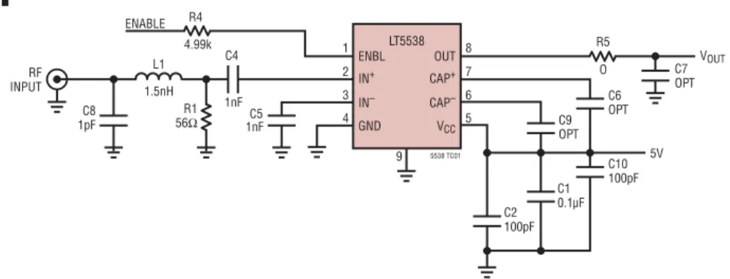
IN– ENBL
EN VOUT
5V
100pF
0.1μF IN+
GND
CAP– OUT CAP+
VCC
LT5538
5538 TA01 1nF
1nF 56 RF INPUT
9
, LT, LTC and LTM are registered trademarks of Linear Technology Corporation. All other trademarks are the property of their respective owners.
5538 TA02 INPUT POWER (dBm)
–75 VOUT
(V)
LINEARITY ERROR (dB)
–65 –55 –45 –35 –25 –15 –5 5
0.2 0.5 0.8 1.1 1.4 2.0 1.7
–3 –2 –1 0 1 3 2
TA = –40°C
TA = 25°C
TA = 85°C
2
5538f
PIN CONFIGURATION
ABSOLUTE MAXIMUM RATINGS
Power Supply Voltage ...5.5V
Enable Voltage ...–0.3V, V
CC+ 0.3V
RF Input Power ...15dBm
Operating Ambient Temperature ... –40°C to +85°C
Storage Temperature Range ... –65°C to +125°C
Maximum Junction Temperature... 150°C
(Note 1)
ORDER INFORMATION
ELECTRICAL CHARACTERISTICS
The
●denotes the specifi cations which apply over the full operating
temperature range, otherwise specifi cations are at T
A= 25°C, V
CC= 5V, ENBL = 5V. (Note 2)
SYMBOL PARAMETER CONDITIONS MIN TYP MAX UNITS
RF Input
Input Frequency Range 40 to 3800 MHz
DC Common Mode Voltage VCC –0.5 V
Input Resistance 394 Ω
fRF = 40 MHZ
RF Input Power Range –75 to 10 dBm
Linear Dynamic Range ±1dB Linearity Error (Note 3) 76 dB
Output Slope 19.9 mV/dB
Logarithmic Intercept (Note 5) –87.5 dBm
Sensitivity –72 dBm
Output Variation vs Temperature Normalized to Output at 25°C PIN = –50dBm; –40°C < TA < 85°C PIN = –30dBm; –40°C < TA < 85°C PIN = –10dBm; –40°C < TA < 85°C
● ● ●
0.1/0.6 –0.1/0.6 –0.2/0.6
dB dB dB
LEAD FREE FINISH TAPE AND REEL PART MARKING PACKAGE DESCRIPTION TEMPERATURE RANGE
LT5538IDD#PBF LT5538IDD#TRPBF LCVG 8-Lead (3mm × 3mm) Plastic DFN –40°C to 85°C
Consult LTC Marketing for parts specifi ed with wider operating temperature ranges. Consult LTC Marketing for information on non-standard lead based fi nish parts. For more information on lead free part marking, go to: http://www.linear.com/leadfree/
For more information on tape and reel specifi cations, go to: http://www.linear.com/tapeandreel/
TOP VIEW
DD PACKAGE 8-LEAD (3mm × 3mm) PLASTIC DFN
5 6 7 8
4 3 2 1 ENBL
IN+ IN– GND
OUT CAP+ CAP– VCC
θJA = 43°C/W
3
5538f
ELECTRICAL CHARACTERISTICS
The
●denotes the specifi cations which apply over the full operating
temperature range, otherwise specifi cations are at T
A= 25°C, V
CC= 5V, ENBL = 5V. (Note 2)
SYMBOL PARAMETER CONDITIONS MIN TYP MAX UNITS
2nd Order Harmonic Distortion Pin = –10dBm; At RF Input –62 dBc
3rd Order Harmonic Distortion Pin = –10dBm; At RF Input –61 dBc
fRF = 450 MHz
RF Input Power Range –75 to 10 dBm
Linear Dynamic Range ±1 dB Linearity Error (Note 3) 75 dB
Output Slope 19.6 mV/dB
Logarithmic Intercept (Note 5) –87.3 dBm
Sensitivity –71.5 dBm
Output Variation vs Temperature Normalized to Output at 25°C
PIN = –50dBm; –40°C < TA < 85°C
PIN = –30dBm; –40°C < TA < 85°C
PIN = –10dBm; –40°C < TA < 85°C
● ● ●
0.1/0.6 0.1/0.5 –0.1/0.5
dB dB dB
2nd Order Harmonic Distortion Pin = –10dBm; At RF Input –43 dBc
3rd Order Harmonic Distortion Pin = –10dBm; At RF Input –44 dBc
fRF = 880 MHz
RF Input Power Range –75 to 10 dBm
Linear Dynamic Range ±1 dB Linearity Error (Note 3) 75 dB
Output Slope 19.0 mV/dB
Logarithmic Intercept (Note 5) –88.8 dBm
Sensitivity –71.5 dBm
Output Variation vs Temperature Normalized to Output at 25°C
PIN = –50dBm; –40°C < TA < 85°C
PIN = –30dBm; –40°C < TA < 85°C
PIN = –10dBm; –40°C < TA < 85°C
● ● ●
0.1/0.7 0.1/0.4 0.1/0.4
dB dB dB
2nd Order Harmonic Distortion Pin = –10dBm; At RF Input –37 dBc
3rd Order Harmonic Distortion Pin = –10dBm; At RF Input –40 dBc
fRF = 2140 MHz
RF Input Power Range –72 to 10 dBm
Linear Dynamic Range ±1 dB Linearity Error (Note 3) 70 dB
Output Slope 17.7 mV/dB
Logarithmic Intercept (Note 5) –89.0 dBm
Sensitivity –69.0 dBm
Output Variation vs Temperature Normalized to Output at 25°C
PIN = –50dBm; –40°C < TA < 85°C
PIN = –30dBm; –40°C < TA < 85°C
PIN = –10dBm; –40°C < TA < 85°C
● ● ●
0.3/0.4 0.4/0.1 0.7/0.5
dB dB dB
fRF = 2700 MHz
RF Input Power Range –72 to 10 dBm
Linear Dynamic Range ±1 dB Linearity Error (Note 3) 65 dB
Output Slope 17.6 mV/dB
4
5538f
Note 1: Stresses beyond those listed under Absolute Maximum Ratings may cause permanent damage to the device. Exposure to any Absolute Maximum Rating condition for extended periods may affect device reliability and lifetime.
Note 2: Specifi cations over the –40°C to 85°C temperature range are assured by design, characterization and correlation with statistical process control.
Note 3: The linearity error is calculated by the difference between the incremental slope of the output and the average slope from –50dBm
to –20dBm. The dynamic range is defi ned as the range over which the linearity error is within ±1dB.
Note 4: Sensitivity is defi ned as the minimum input power required for the linearity error within 3dB of the ideal log-linear transfer curve.
Note 5: Logarithmic Intercept is an extrapolated input power level from the best-fi tted log-linear straight line, where the output voltage is 0V.
SYMBOL PARAMETER CONDITIONS MIN TYP MAX UNITS
Sensitivity –69.5 dBm
Output Variation vs Temperature Normalized to Output at 25°C
PIN = –50dBm; –40°C < TA < 85°C
PIN = –30dBm; –40°C < TA < 85°C
PIN = –10dBm; –40°C < TA < 85°C
● ● ●
0.3/0.3 0.7/–0.3 1.1/–0.9
dB dB dB
fRF = 3600 MHz
RF Input Power Range –65 to 10 dBm
Linear Dynamic Range ±1 dB Linearity Error (Note 3) 57 dB
Output Slope 18 mV/dB
Logarithmic Intercept (Note 5) –81.4 dBm
Sensitivity –63 dBm
Output Variation vs Temperature Normalized to Output at 25°C
PIN = –45dBm; –40°C < TA < 85°C
PIN = –25dBm; –40°C < TA < 85°C
PIN = –5dBm; –40°C < TA < 85°C
● ● ●
0.6/–0.3 0.9/–0.6 1.4/–1.2
dB dB dB
Output Interface
Output DC Voltage No RF Signal Present 0.350 V
Output Impedance 150 Ω
Source Current 10 mA
Sink Current 200 μA
Rise Time 0.5V to 1.6V, 10% to 90%, fRF = 880 MHz 100 ns
Fall Time 1.6V to 0.5V, 10% to 90%, fRF = 880 MHz 180 ns
Power Up/Down
ENBL = High (On) ● 1 V
ENBL = Low (Off) ● 0.3 V
ENBL Input Current VENBL = 5V 205 μA
Turn ON time 300 ns
Turn OFF Time 1 μs
Power Supply
Supply Voltage 3 5.25 V
Supply Current 29 36 mA
Shutdown Current ENBL = Low 1 100 μA
ELECTRICAL CHARACTERISTICS
The
●denotes the specifi cations which apply over the full operating
temperature range, otherwise specifi cations are at T
A= 25°C, V
CC= 5V, ENBL = 5V. (Note 2)
5
5538f
TYPICAL PERFORMANCE CHARACTERISTICS
Supply Current vs Supply Voltage
Output Voltage, Linearity Error vs
Input Power at 40MHz
V
OUTVariation vs Input Power at
40MHz
Output Voltage, Linearity Error vs
Input Power at 450MHz
Output Voltage, Linearity Error vs
Input Power at 2.14GHz
V
OUTVariation vs Input Power at
2.14GHz
(Test Circuit shown in Figure 5)
V
OUTVariation vs Input Power at
450MHz
Output Voltage, Linearity Error vs
Input Power at 880MHz
V
OUTVariation vs Input Power at
880MHz
5538 G01
SUPPLY VOLTAGE VCC (V)
2.5 10
SUPPLY CURRENT I
CC (mA) 15 20 25 30 40
3 3.5 4 4.5 5 5.5
35
TA = –40°C
TA = 25°C
TA = 85°C
5538 G02 INPUT POWER (dBm)
–75 0.2 VOUT
(V)
LINEARITY ERROR (dB)
0.5 0.8 1.1 1.4 2.0
–65 –55 –45 –35 –25 –15 –5 5
1.7 –3 –2 –1 0 1 3 2
TA = –40°C
TA = 25°C
TA = 85°C
VCC = 5V
5538 G03 INPUT POWER (dBm)
–75 VOUT
VARIATION (dB)
–65 –55 –45 –35 –25 –15 –5 5
–3 –2 –1 0 1 3 2
TA = –40°C
TA = 85°C
VCC = 5V
NORMALIZED AT 25°C
5538 G04 INPUT POWER (dBm)
–75 VOUT
(V)
LINEARITY ERROR (dB)
–65 –55 –45 –35 –25 –15 –5 5
0.2 0.5 0.8 1.1 1.4 2.0 1.7 –3 –2 –1 0 1 3 2
TA = –40°C
TA = 25°C
TA = 85°C
VCC = 5V
5538 G05 INPUT POWER (dBm)
–75 VOUT
VARIATION (dB)
–65 –55 –45 –35 –25 –15 –5 5
–3 –2 –1 0 1 3 2
TA = –40°C
TA = 85°C
VCC = 5V
NORMALIZED AT 25°C
5538 G06 INPUT POWER (dBm)
–75 VOUT
(V)
LINEARITY ERROR (dB)
–65 –55 –45 –35 –25 –15 –5 5
0.2 0.5 0.8 1.1 1.4 2.0 1.7 –3 –2 –1 0 1 3 2
TA = –40°C
TA = 25°C
TA = 85°C
VCC = 5V
5538 G07 INPUT POWER (dBm)
VOUT
VARIATION (dB)
–65
–75 –55 –45 –35 –25 –15 –5 5
–3 –2 –1 0 1 3 2
TA = –40°C
TA = 85°C
VCC = 5V
NORMALIZED AT 25°C
5538 G08 INPUT POWER (dBm)
–75 VOUT
(V)
LINEARITY ERROR (dB)
–65 –55 –45 –35 –25 –15 –5 5
0.2 0.5 0.8 1.1 1.4 2.0 1.7 –3 –2 –1 0 1 3 2
TA = –40°C
TA = 25°C
TA = 85°C
VCC = 5V
5538 G09 INPUT POWER (dBm)
VOUT
VARIATION (dB)
–65
–75 –55 –45 –35 –25 –15 –5 5
–3 –2 –1 0 1 3 2
TA = –40°C
TA = 85°C
VCC = 5V
6
5538f
TYPICAL PERFORMANCE CHARACTERISTICS
V
OUTVariation vs Input Power at
2.7GHz
Output Voltage, Linearity Error vs
Input Power at 3.6GHz
V
OUTVariation vs Input Power at
3.6GHz
Slope Distribution vs
Temperature at 2.14GHz
Output Voltage, Linearity Error vs
Input Power at 2.7GHz
Logarithmic Intercept Distribution
vs Temperature at 2.14GHz
(Test Circuit shown in Figure 5)
5538 G10 INPUT POWER (dBm)
–70 VOUT
(V)
LINEARITY ERROR (dB)
–60 –50 –40 –30 –20 –10 0 10
0 0.3 0.6 0.9 1.2 1.8 1.5 –3 –2 –1 0 1 3 2
TA = –40°C
TA = 25°C
TA = 85°C
VCC = 5V
5538 G11 INPUT POWER (dBm)
VOUT
VARIATION (dB)
–60
–70 –50 –40 –30 –20 –10 0 10
–3 –2 –1 0 1 3 2
TA = –40°C
TA = 85°C
VCC = 5V
NORMALIZED AT 25°C
5538 G12 INPUT POWER (dBm)
VOUT
(V)
LINEARITY ERROR (dB)
–65 –55 –45 –35 –25 –15 –5 5
0 0.3 0.6 0.9 1.2 1.8 1.5 –3 –2 –1 0 1 3 2
TA = –40°C
TA = 25°C
TA = 85°C
VCC = 5V
5538 G13 INPUT POWER (dBm)
VOUT
VARIATION (dB)
–60
–70 –50 –40 –30 –20 –10 0 10
–3 –2 –1 0 1 3 2
TA = –40°C
TA = 85°C
VCC = 5V
NORMALIZED AT 25°C
Output Voltage, Linearity Error vs
V
CC@40MHz
Output Voltage, Linearity Error vs
V
CC@2140MHz
Output Voltage, Linearity Error vs
V
CC@3600MHz
5538 G16 INPUT POWER (dBm)
–75 VOUT
(V)
LINEARITY ERROR (dB)
–65 –55 –45 –35 –25 –15 –5 5
0.2 0.5 0.8 1.1 1.4 2.0 1.7 –3 –2 –1 0 1 3 2
VCC = 5V
VCC = 3V
NORMALIZED AT 5V
5538 G17 INPUT POWER (dBm)
–75 VOUT
(V)
LINEARITY ERROR (dB)
–65 –55 –45 –35 –25 –15 –5 5
0.2 0.5 0.8 1.1 1.4 2.0 1.7 –3 –2 –1 0 1 3 2
VCC = 5V
VCC = 3V
NORMALIZED AT 5V
5538 G18 INPUT POWER (dBm)
VOUT
(V)
LINEARITY ERROR (dB)
–65 –55 –45 –35 –25 –15 –5 5
0 0.3 0.6 0.9 1.2 1.8 1.5 –3 –2 –1 0 1 3 2
VCC = 5V
VCC = 3V
VCC = 5V
5538 G15 LOGARITHMIC INTERCEPT (dBm)
PERCENTAGE DISTRIBUTION (%)
–78 –80 –82 –84 –86 –88 –90 –92 –94 –96 –98 0 2 4 6 8 12 10 14 16
TA = –40°C
TA = 25°C
TA = 85°C
5538 G14 SLOPE (mV/dB)
PERCENTAGE DISTRIBUTION (%)
20 20.8 19.2 18.4 17.6 16.8 16 0 5 10 15 20 30 25 35 40
TA = –40°C
TA = 25°C
7
5538f
PIN FUNCTIONS
ENBL (Pin 1):
Enable Pin. An applied voltage above 1V will
activate the bias for the IC. For an applied voltage below
0.3V, the circuits will be shut down (disabled) with a
cor-responding reduction in power supply current. If the enable
function is not required, then this pin can be connected
to V
CC. Typical enable pin input currents are 100μA for
EN = 3V and 200μA for EN = 5V, respectively. Note that at
no time should the ENBL pin voltage be allowed to exceed
V
CCby more than 0.3V.
IN
+(Pin 2):
RF Input Pin. The pin is internally biased to
V
CC–0.5V and should be DC blocked externally. The input
is connected via internal 394Ω resistor to the IN
–pin which
should be connected to ground with an ac-decoupling
capacitor.
IN
–(Pin 3):
AC Ground Pin. The pin is internally biased to
V
CC–0.5V and coupled to ground via internal 20pF capacitor.
This pin should be connected to ground with an external
ac-decoupling capacitor for low frequency operation.
GND (Pin 4, Exposed Pad Pin 9):
Circuit Ground Return
for the entire IC. This pin must be soldered to the printed
circuit board ground plane.
V
CC(Pin 5):
Power Supply Pin. This pin should be
de-coupled using 100pF and 0.1μF capacitors.
CAP
–, CAP
+(Pins 6, 7):
Optional Filter Capacitor Pins.
These pins are internally connected to the detector outputs
in front of the output buffer amplifi er. An external low-pass
fi ltering can be formed by connecting a capacitor to Vcc
from each pin for fi ltering a low frequency modulation
sig-nal. See the Applications Information section for detail.
OUT (Pin 8):
Detector DC Output Pin.
BLOCK DIAGRAM
RF LIMITER IN+
IN–
GND
RF LIMITER
RF DETECTOR CELLS DC OFFSET CANCELLATION
RF LIMITER RF LIMITER RF LIMITER
CAP–CAP+ 3
2
4 9 6 7
OUT 8
ENBL 1
VCC
5
8
5538f
The LT5538 is a 40MHz to 3.8 GHz logarithmic RF power
detector. It consists of cascaded limiting amplifi ers and
RF detectors. The output currents from every RF detector
are combined and low-pass fi ltered before applied to the
output buffer amplifi er. As a result, the fi nal DC output
voltage approximates the logarithm of the amplitude of the
input signal. The LT5538 is able to accurately measure an
RF signal over a 70dB dynamic range (–68dBm to 2dBm
at 2.1GHz) with 50Ω single-ended input impedance. The
slope of linear to log transfer function is about 17.7mV/dB
at 2.1GHz. Within the linear dynamic range, very stable
output is achieved over the full temperature range from
–40°C to 85°C and over the full operating frequency
range from 40MHz to 3.8GHz. The absolute variation over
temperature is typically within ±1dB over 65dB dynamic
range at 2.1GHz.
RF INPUT
The simplifi ed schematic of the input circuit is shown in
Figure 1. The IN
+and IN
–pins are internally biased to
V
CC–0.5V. The IN
–pin is internally coupled to ground via
20pF capacitor. An external capacitor of 1nF is needed to
connect this pin to ground for low frequency operation.
The impedance between IN
+and IN
–is about 394Ω. The
RF input pin IN
+should be DC blocked when connected
to ground or other matching components. A 56Ω resistor
(R1) connected to ground will provide better than 10dB
input return loss over the operating frequency range up
to 1.5GHz. At higher operating frequency, additional LC
matching elements are needed for a proper impedance
matching to a 50Ω source as shown in Figure 2. Refer to
Figure 6 for the circuit schematic of the input matching
network. The input impedance vs frequency of the RF input
port IN
+is detailed in Table 1.
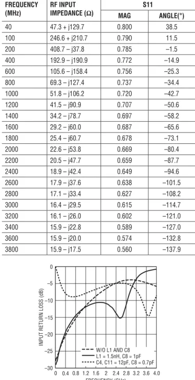
Table 1. RF Input Impedance
FREQUENCY (MHz)
RF INPUT IMPEDANCE (Ω)
S11
MAG ANGLE(°)
40 47.3 + j129.7 0.800 38.5
100 246.6 + j210.7 0.790 11.5
200 408.7 – j37.8 0.785 –1.5
400 192.9 – j190.9 0.772 –14.9
600 105.6 – j158.4 0.756 –25.3
800 69.3 – j127.4 0.737 –34.4
1000 51.8 – j106.2 0.720 –42.7
1200 41.5 – j90.9 0.707 –50.6
1400 34.2 – j78.7 0.697 –58.2
1600 29.2 – j60.0 0.687 –65.6
1800 25.4 – j60.7 0.678 –73.1
2000 22.6 – j53.8 0.669 –80.4
2200 20.5 – j47.7 0.659 –87.7
2400 18.9 – j42.4 0.649 –94.6
2600 17.9 – j37.6 0.638 –101.5
2800 17.1 – j33.4 0.627 –108.2
3000 16.4 – j29.5 0.615 –114.7
3200 16.1 – j26.0 0.602 –121.0
3400 15.9 – j22.8 0.589 –127.0
3600 15.9 – j20.0 0.574 –132.8
3800 15.9 – j17.5 0.560 –137.9
APPLICATIONS INFORMATION
5.3k
394 IN+
IN–
20p 5.3k
VCC
+
–
5538 F01
Figure 1. Simplifi ed Schematic of the Input Circuit
Figure 2. Input Return Loss with Additional LC Matching Network
5538 F02 FREQUENCY (GHz)
0
INPUT RETURN LOSS (dB)
0.4 0.8 1.2 1.6 2 2.4 2.8 3.2 3.6 4.0
–30 –25 –20 –15 –10 0 –5
W/O L1 AND C8 L1 = 1.5nH, C8 = 1pF C4, C11 = 12pF, C8 = 0.7pF
9
5538f
APPLICATIONS INFORMATION
OUTPUT INTERFACE
The output interface of the LT5538 is shown in Figure 3.
This output buffer circuit can source 10mA current to the
load and sink 200 μA current from the load. The
small-signal output bandwidth is approximately 4MHz when the
output is resistively terminated or open. The full-scaled
10% to 90% rise and fall times are 100nS and 180nS,
respectively. The output transient responses at varied
input power levels are shown in Figure 4.
When the part is enabled, the output impedance is about
150Ω. When it is disabled, the output impedance is about
29.5kΩ referenced to ground.
EXTERNAL FILTERING AT CAP
+, CAP
–The CAP
+and CAP
–Pins are internally biased at V
CC–0.36V
via a 200Ω resistor from voltage supply V
CCas shown in
Figure 3. These two pins are connected to the differential
outputs of the internal RF detector cells. In combination
with the 20pF in parallel, a low-pass fi lter is formed with
–3dB corner frequency of 20MHz. The high frequency
rectifi ed signals (particularly second-order harmonic of
the RF signal) from the detector cells are fi ltered and then
the DC output is amplifi ed by the output buffer amplifi er. In
some applications, the LT5538 may be used to measure a
modulated RF signal with low frequency AM content (lower
than 20MHz), a large modulation signal may be present
at these two pins due to insuffi cient low-pass fi ltering,
resulting in output voltage fl uctuation at the LT5538’s
output. Its DC content may also vary depending upon the
modulation frequency. To assure stable DC output of the
LT5538, external capacitors C6 and C9 can be connected
from CAP
+and CAP
–to V
CCto fi lter out this low frequency
AM modulation signal. Assume the modulation frequency
of the RF signal is f
MOD, the capacitor value in Farads of
C6 and C9 can be chosen by the following formula:
C6 (or C9) ≥ 10/(2π • 200 • f
MOD)
Do not connect these two fi ltering capacitors to ground
or any other low voltage reference at any time to avoid an
abnormal start-up condition.
Figure 3. Simplifi ed Schematic of the Output Interface
Figure 4. Simplifi ed Circuit Schematic of the Output Interface
200
CAP+ C9
CAP–
200
100μA
150
OUT
200μA OUTPUT CURRENTS
FROM RF DETECTORS LT5538 VCC
5538 F03
20p
+ –
+ –
+ –
C6
5538 F04 TIME (μs)
PIN = 0dBm PIN = 10dBm PIN = 20dBm PIN = 30dBm PIN = 40dBm PIN = 50dBm VOUT
(V)
RF PULSE ENABLE (V)
0 0.2 0.4 0.6 0.8 1.0 1.2 1.4 1.6 1.8 2.0
0 0.5 1.0 1.5 2.0 3.0
2.5
–18 –14 –10 –6 –2 6
2 AT 880MHZ
RF PULSE OFF RF PULSE OFF
10
5538f
APPLICATIONS INFORMATION
ENBL (ENABLE) PIN OPERATION
A simplifi ed circuit schematic of the ENBL Pin is shown
in Figure 5. The enable voltage necessary to turn on the
LT5538 is 1V. The current drawn by the ENBL pin varies
with the voltage applied at the pin. When the ENBL
volt-age is 3V, the ENBL current is typically 100 μA. When the
ENBL voltage is 5V, the ENBL current is increased to 200
μA. To disable or turn off the chip, this voltage should be
below 0.3V. It is important that the voltage applied to the
ENBL pin should never exceed V
CCby more than 0.3V.
Otherwise, the supply current may be sourced through the
upper ESD protection diode connected at the ENBL pin.
Under no circumstances should voltage be applied to the
ENBL Pin before the supply voltage is applied to the V
CCpin. If this occurs, damage to the IC may result.
Figure 5. Simplifi ed Schematic of the Enable Circuit
Figure 6. Evaluation Board Circuit Schematic
40MHz to 2.7GHz
REF DES VALUE SIZE PART NUMBER
C1 0.1μF 0603 AVX 0603ZC104KAT
C2, C10 100pF 0402 AVX 0402YC101KAT
C4, C5 1nF 0603 AVX 0402ZC102K
C8 1pF 0402 AVX 0402YA1ROCAT
R1 56 0402 VISHAY, CRCW040256ROFKED
R4 4.99k 0402 VISHAY, CRCW04024K99FKED
L1 1.5nH 0402 TOKO, LL1005-FH2IN5S
TEST CIRCUIT
42k 42k
ENBL VCC
5538 F05
IN– ENBL 1 ENABLE
C5 C4 L1
1.5nH R4
4.99k R5
5V O
VOUT
2 3 4
9 8 7 6
5 C9
OPT IN+
GND
CAP– OUT CAP+
VCC
LT5538
5538 TC01 1nF
1nF R1 56Ω RF
INPUT C8 1pF
C6 OPT
C7 OPT
C1 0.1μF
C10 100pF
C2 100pF
3.6GHz to 3.8GHz
REF DES VALUE SIZE PART NUMBER
C4, C11 12pF 0402 MURATA, GRM155C1H120JZ01B
C8 0.7pF 0402 MURATA, GJR155C1HR70BB01
C5 OPEN
11
5538f
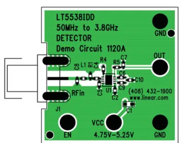
TEST CIRCUIT
Figure 7. Component Side of Evalution Board
PACKAGE DESCRIPTION
3.00±0.10
(4 SIDES)
NOTE:
1. DRAWING TO BE MADE A JEDEC PACKAGE OUTLINE M0-229 VARIATION OF (WEED-1) 2. DRAWING NOT TO SCALE
3. ALL DIMENSIONS ARE IN MILLIMETERS
4. DIMENSIONS OF EXPOSED PAD ON BOTTOM OF PACKAGE DO NOT INCLUDE MOLD FLASH. MOLD FLASH, IF PRESENT, SHALL NOT EXCEED 0.15mm ON ANY SIDE 5. EXPOSED PAD SHALL BE SOLDER PLATED
6. SHADED AREA IS ONLY A REFERENCE FOR PIN 1 LOCATION ON TOP AND BOTTOM OF PACKAGE
0.38± 0.10
BOTTOM VIEW—EXPOSED PAD
1.65± 0.10
(2 SIDES)
0.75±0.05
R = 0.115 TYP
2.38±0.10
(2 SIDES) 1 4
8 5
PIN 1 TOP MARK (NOTE 6)
0.200 REF
0.00 – 0.05
(DD8) DFN 1203
0.25± 0.05
2.38±0.05
(2 SIDES)
RECOMMENDED SOLDER PAD PITCH AND DIMENSIONS
1.65±0.05
(2 SIDES)
2.15±0.05
0.50 BSC
0.675±0.05
3.5±0.05
PACKAGE OUTLINE
0.25± 0.05
0.50 BSC
DD Package
8-Lead Plastic DFN (3mm
×
3mm)
(Reference LTC DWG # 05-08-1698)
Information furnished by Linear Technology Corporation is believed to be accurate and reliable. However, no responsibility is assumed for its use. Linear Technology Corporation makes no representa-tion that the interconnecrepresenta-tion of its circuits as described herein will not infringe on existing patent rights.
12
5538f
Linear Technology Corporation
1630 McCarthy Blvd., Milpitas, CA 95035-7417
(408) 432-1900 ● FAX: (408) 434-0507 ● www.linear.com © LINEAR TECHNOLOGY CORPORATION 2008
LT 0408 • PRINTED IN USA
RELATED PARTS
PART NUMBER DESCRIPTION COMMENTS Infrastructure
LT5514 Ultralow Distortion, IF Amplifi er/ADC Driver with Digitally
Controlled Gain
850MHz Bandwidth, 47 dBm OIP3 at 100MHz, 10.5dB to 33dB Gain Control Range
LT5515 1.5GHz to 2.5GHz Direct Conversion Quadrature Demodulator 20dBm IIP3, Integrated LO Quadrature Generator
LT5516 0.8GHz to 1.5GHz Direct Conversion Quadrature Demodulator 21.5dBm IIP3, Integrated LO Quadrature Generator
LT5517 40MHz to 900MHz Quadrature Demodulator 21dBm IIP3, Integrated LO Quadrature Generator
LT5518 1.5GHz to 2.4GHz High Linearity Direct Quadrature
Modulator 22.8dBm OIP3 at 2GHz, –158.2dBm/Hz Noise Floor, 50Ω Single-Ended RF and LO Ports, 4-Channel W-CDMA ACPR = –64dBc at 2.14GHz
LT5519 0.7GHz to 1.4GHz High Linearity Upconverting Mixer 17.1dBm IIP3 at 1GHz, Integrated RF Output Transformer with 50Ω
Matching, Single-Ended LO and RF Ports Operation
LT5520 1.3GHz to 2.3GHz High Linearity Upconverting Mixer 15.9dBm IIP3 at 1.9GHz, Integrated RF Output Transformer with 50Ω
Matching, Single-Ended LO and RF Ports Operation
LT5521 10MHz to 3700MHz High Linearity Upconverting Mixer 24.2dBm IIP3 at 1.95GHz, NF = 12.5dB, 3.15V to 5.25V Supply,
Single-Ended LO Port Operation
LT5522 600 MHz to 2.7GHz High Signal Level Downconverting
Mixer
4.5V to 5.25V Supply, 25dBm IIP3 at 900MHz, NF = 12.5dB, 50Ω Single-Ended RF and LO Ports
LT5524 Low Power, Low Distortion ADC Driver with Digitally
Programmable Gain
450MHz Bandwidth, 40dBm OIP3, 4.5dB to 27dB Gain Control
LT5525 High Linearity, Low Power Downconverting Mixer Single-Ended 50Ω RF and LO Ports, 17.6dBm IIP3 at 1900MHz, ICC = 28mA
LT5526 High Linearity, Low Power Downconverting Mixer 3V to 5.3V Supply, 16.5dBm IIP3, 100kHz to 2GHz RF, NF = 11dB,
ICC = 28mA, –65dBm LO-RF Leakage
LT5527 400MHz to 3.7GHz High Signal Level Downconverting
Mixer IIP3 = 23.5dBm and NF = 12.5dBm at 1900MHz, 4.5V to 5.25V Supply, ICC = 78mA, Conversion Gain = 2dB
LT5528 1.5GHz to 2.4GHz High Linearity Direct Quadrature
Modulator 21.8dBm OIP3 at 2GHz, –159.3dBm/Hz Noise Floor, 50Ω, 0.5VInterface, 4-Channel W-CDMA ACPR = –66dBc at 2.14GHz DC Baseband
LT5557 400MHz to 3.8GHz, 3.3V High Signal Level
Downconverting Mixer
IIP3 = 23.7dBm at 2600MHz, 23.5dBm at 3600MHz, ICC = 82mA at 3.3V
LT5560 Ultra-Low Power Active Mixer 10mA Supply Current, 10dBm IIP3, 10dB NF, Usable as Up- or Down-Converter.
LT5568 700MHz to 1050MHz High Linearity Direct Quadrature
Modulator 22.9dBm OIP3 at 850MHz, –160.3dBm/Hz Noise Floor, 50Ω, 0.5VBaseband Interface, 3-Ch CDMA2000 ACPR = –71.4dBc at 850MHzDC
LT5572 1.5GHz to 2.5GHz High Linearity Direct Quadrature
Modulator 21.6dBm OIP3 at 2GHz, –158.6dBm/Hz Noise Floor, High-Ohmic 0.5VBaseband Interface, 4-Ch W-CDMA ACPR = –67.7dBc at 2.14GHz DC
LT5575 800MHz to 2.7GHz High Linearity Direct Conversion I/Q
Demodulator 50Ω, Single-Ended RF and LO Inputs. 28dBm IIP3 at 900MHz, 13.2dBm P1dB, 0.04dB I/Q Gain Mismatch, 0.4° I/Q Phase Mismatch
RF Power Detectors
LTC®
5505 RF Power Detectors with >40dB Dynamic Range 300MHz to 3GHz, Temperature Compensated, 2.7V to 6V Supply
LTC5507 100kHz to 1000MHz RF Power Detector 100kHz to 1GHz, Temperature Compensated, 2.7 to 6V Supply
LTC5508 300MHz to 7GHz RF Power Detector 44dB Dynamic Range, Temperature Compensated, SC70 Package
LTC5509 300MHz to 3GHz RF Power Detector 36dB Dynamic Range, Low Power Consumption, SC70 Package
LTC5530 300MHz to 7GHz Precision RF Power Detector Precision VOUT Offset Control, Shutdown, Adjustable Gain
LTC5531 300MHz to 7GHz Precision RF Power Detector Precision VOUT Offset Control, Shutdown, Adjustable Offset
LTC5532 300MHz to 7GHz Precision RF Power Detector Precision VOUT Offset Control, Adjustable Gain and Offset
LT5534 50MHz to 3GHz Log RF Power Detector with 60dB
Dynamic Range ±1dB Output Variation over Temperature, 38ns Response Time, Log Linear Response
LTC5536 Precision 600Mhz to 7GHz RF Power Detector with Fast
Comparator Output 25ns Response Time, Comparator Reference Input, Latch Enable Input, –26dBm to +12dBm Input Range
LT5537 Wide Dynamic Range Log RF/IF Detector Low Frequency to 1GHz, 83dB Log Linear Dynamic Range
LT5570 2.7GHz RMS Power Detector Fast Responding, up to 60dB Dynamic Range, ±0.3dB Accuracy Over