MetalMUMPs
Design
Handbook
a MUMPs
®process
Allen Cowen, Bruce Dudley, Ed Hill, Mark Walters, Robert Wood,
Stafford Johnson, Henry Wynands, and Busbee Hardy
MEMSCAP
E L E C T R O P L A T E D N I C K E L M I C R O M A C H I N I N G P R O C E S S
Copyright © 2002 by MEMScAP. All rights reserved.
Permission to use, copy, and modify for internal, noncommercial purposes is hereby granted. Any distribution of this manual or associated layouts or any part thereof is strictly prohibited without prior written consent of MEMScAP Inc.
GDSII is a trademark of Calma, Valid, Cadence.
L-EDIT and TANNER database are trademarks of Tanner Research Inc.
Table of Contents
Chapter 1
Electroplated Nickel Micromachining Process... 1
1.1. Introduction ... 1
1.2. Process Overview ... 2
1.3. MetalMUMPs Process Flow ... 5
Chapter 2 MetalMUMPs Design Rules and Considerations ... 13
2.1. Introduction ... 13
2.2. Allowable Layer Combinations... 14
2.3. Design Rules ... 20
2.4. Beyond the Design Rules... 31
2.5. Film Parameters ... 34
2.6. Layout Requirements ... 34
2.7. Layout Submission ... 35
E L E C T R O P L A T E D N I C K E L M I C R O M A C H I N I N G P R O C E S S
Chapter 1
Electroplated Nickel Micromachining Process
1.1.
Introduction
The Multi-User MEMS Processes, or MUMPs®, is a commercial program that provides cost-effective, proof-of-concept MEMS fabrication to industry, universities, and government worldwide. MEMSCAP offers three standard processes as part of the MUMPs® program: PolyMUMPs, a three-layer polysilicon surface micromachining process: MetalMUMPs, an electroplated nickel process; and SOIMUMPs, a silicon-on-insulator micromachining process.
The following is a general process description and user guide for MetalMUMPs, which is designed for general-purpose electroplated nickel micromachining of MEMS. Chapter 1 of this document explains the process step-by-step, while Chapter 2 outlines the design rules for the process.
Though this document is geared toward designers who do not have a strong background in microfabrication, it contains information that is useful to all MetalMUMPs users. Regardless of the level of the designer, we strongly recommend all users of PolyMUMPs review this document prior to submitting a design.
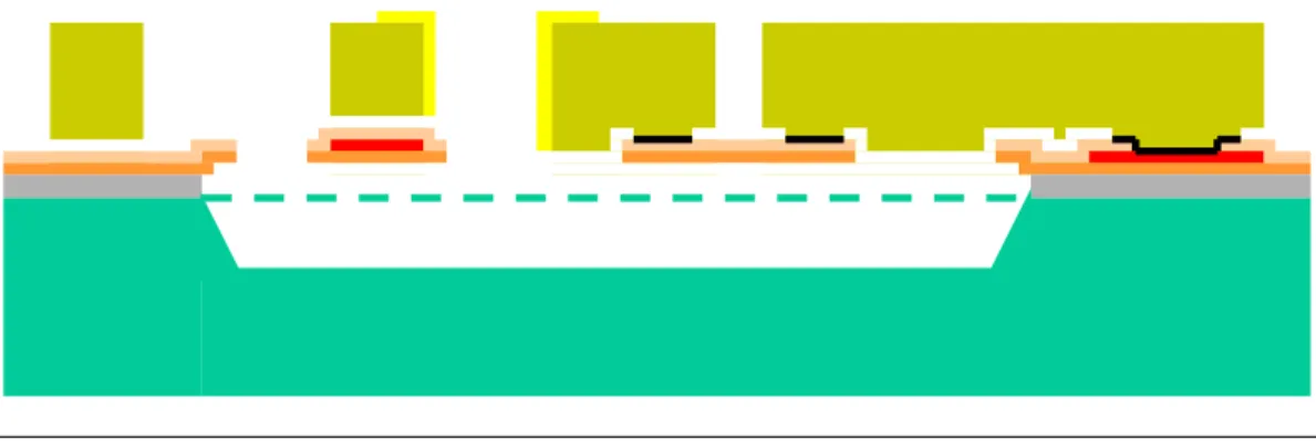
C H A P T E R 1
F I G U R E 1 . 1. Cross sectional view of a microrelay fabricated using all layers of the MetalMUMPs process (figure not to scale).
Figure 1.1 is a cross section of a microrelay fabricated with the MetalMUMPs process. This process has the following general features:
1. Electroplated nickel is used as the primary structural material and electrical interconnect layer
2. Doped polysilicon can be used for resistors, additional mechanical structures, and/or cross-over
electrical routing
3. Silicon nitride is used as an electrical isolation layer 4. Deposited oxide (PSG) is used for the sacrificial layers
5. A trench layer in the silicon substrate can be incorporated for additional thermal and electrical
isolation
6. Gold overplate can be used to coat the sidewalls of nickel structures with a low contact resistance
material
The process is designed to be as general as possible, and to be capable of supporting many different designs on a single silicon wafer. Since the process was not optimized with the purpose of fabricating any one specific device, the thicknesses of the structural and sacrificial layers were chosen to suit most users, and the layout design rules were chosen conservatively to guarantee the highest yield possible.
1.2.
Process Overview
MetalMUMPs is an electroplated nickel micromachining process derived from work performed at MEMSCAP (JDSU, Cronos, MCNC) throughout the 1990’s. This process flow was originally developed for the fabrication of MEMS micro-relay devices based on a thermal actuator technology. The process flow described below is designed to introduce inexperienced users to this micromachining process. The text is supplemented by drawings that show the process flow in the context of building a patented microrelay.
Naming Convention: Lithography levels (i.e. names for each masking level) are typed in upper case. Specific layers of material, such as an oxide, polysilicon, or metal layer, are typed in lower case with the first letter capitalized. For
E L E C T R O P L A T E D N I C K E L M I C R O M A C H I N I N G P R O C E S S
example POLY refers to the masking level for patterning the polysilicon layer, Poly. Table 2.1 outlines the material layer names, the thickness of each layer, and the lithography levels associated with each layer.
However, be aware that not every upper case word is necessarily a lithography level. Commonly used acronyms such as PSG (PhosphoSilicate Glass), LPCVD (Low Pressure Chemical Vapor Deposition) are uppercase, as are some chemical symbols such as KOH (chemical symbol for potassium hydroxide).
The MetalMUMPs process flow is described below using the naming convention for the various layers.
1. Base wafer: N-type (100) silicon.
2. Isolation Oxide – A 2 um layer of silicon oxide is grown on the wafer surface to provide electrical
isolation from the substrate.
3. Oxide 1 – This is a 0.5µm thick PSG layer that acts as a sacrificial release layer. The removal of the
Oxide 1 layer at the end of the process releases the Nitride 1 layer (described in # 4). Oxide 1 is lithographically patterned with the first mask level, OXIDE1, and etched. Oxide 1 also defines the regions in which the silicon trench will be formed.
4. Nitride 1 – This is blanket layer of 0.35µm low-stress silicon nitride. Nitride 1 is used in combination
with the subsequent Nitride 2 layer for several purposes. The nitride layers provide a protective encapsulation for the polysilicon. The nitride pattern also defines a protective layer on the substrate that determines where Si trench etching occurs (step 12). Third, a released and patterned nitride area may also be used to provide a mechanical linkage between released Metal structures that must be electrically isolated.
5. Poly – This layer is 0.7µm polysilicon film, which is implant doped and annealed to provide consistent
electrical properties. The Poly layer is patterned with the second mask level, POLY, and etched. This layer can be used to form resistor elements, mechanical structures, or for electrical cross-over routing.
6. Nitride 2 – This is a second layer of 0.35µm thick low-stress silicon nitride. The combination of
Nitride 1 and Nitride 2 layers are lithographically patterned with the third mask level, NITRHOLE, and etched.
7. Oxide 2 – This second sacrificial oxide layer is 1.1µm of PSG. This is removed at the final release step
to free the Metal mechanical layer (step 10). Oxide 2 is patterned with the fourth mask level, METANCH, and is wet chemically etched.
8. Anchor Metal – The Oxide 2 patterning step also provides the pattern for the for the metal structure
anchors. A liftoff process is used to provide thin layers of Cr and Pt (Anchor Metal) only in the bottom of the Oxide 2 anchors.
9. Plating Base – This layer is a blanket metal layer of 500 nm of Cu protected with a thin Ti layer. The
Plating Base layer provides electrical continuity across the wafer for the subsequent Metal electroplating step.
10. Metal - The fifth mask level, METAL, is patterned using a thick resist to form the stencil for the
electroplated Metal layer. 20µm of nickel is electroplated into the patterned resist. Subsequently a
C H A P T E R 1
0.5µm gold layer is plated on top of the nickel to provide a suitable pad material for wire bonding of external electrical connections. This combination of 20µm nickel and 0.5µm gold forms the Metal layer. The Metal layer serves as the primary mechanical layer and electrical interconnect layer.
11. Sidewall Metal – A final plated metal layer, Sidewall Metal, is a 1-3µm gold layer, plated on selected
areas of the sidewall of the Metal layer. This provides a highly reliable low resistance electrical contact and has the effect of shrinking the gaps in adjacent electroplated nickel structures. The process sequence is to first use the sixth mask level, GOLDOVP, to open up an oversized or ‘bloated’ area in a thick photoresist layer where Sidewall Metal is desired. The Plating Base is removed from any exposed regions using wet chemical etching. The desired resist pattern for Sidewall Metal is then processed with a standard sized or “unbloated” version of GOLDOVP. The 1-3µm thick gold Sidewall Metal layer is then electroplated.
12. The final steps are the release and Si trench etch. The release is a series of wet chemical etches to first
remove the Plating Base and then the sacrificial layers and the Isolation oxide layer over the trench areas. Finally, a wet chemical etch of the silicon, using KOH, is used to form a 25µm deep trench in the silicon substrate. This occurs in the areas defined by the OXIDE1 and NITRHOLE masks. This trench provides additional thermal and electrical isolation.
13. The wafers are diced, sorted and shipped to the MetalMUMPs user.
The following pages provide a graphical representation of the process steps.
E L E C T R O P L A T E D N I C K E L M I C R O M A C H I N I N G P R O C E S S
1.3.
MetalMUMPs Process Flow
Oxide 1 Deposited
F I G U R E 1 . 2. A 2µm thick oxide (Isolation Oxide) is grown on the surface of the starting n-type (100) silicon wafer. This is followed by deposition of a 0.5µm thick sacrificial phosphosilicate glass (PSG) layer (Oxide 1).
Oxide 1 Patterned Mask Level: OXIDE1
F I G U R E 1 . 3 The wafers are coated with UV-sensitive photoresist and lithographically patterned by exposing to UV light through the first level mask (OXIDE1), and then developing it. The photoresist in exposed areas is removed, leaving behind a patterned photoresist mask for etching. Wet chemical etching is used to remove the unwanted sacrificial PSG. After the etch, the photoresist is chemically stripped. This method of patterning the wafers with photoresist, etching and stripping the remaining photoresist is used repeatedly in the MetalMUMPs process.
MetalMUMPs Design Handbook, Rev. 1.0 5
Substrate Oxide 1 Poly Oxide 2 Metal
Isolation Oxide Nitride 1 Nitride 2 Anchor Metal Sidewall Metal
C H A P T E R 1
Nitride 1 and Poly Deposited
F I G U R E 1 . 4. A 0.35µm layer of silicon nitride (Nitride 1) is deposited, followed immediately by the deposition of a 0.7µm layer of polysilicon (Poly).
Poly Patterned Mask Level: POLY
F I G U R E 1 . 5 . The wafers are coated with photoresist and the second level (POLY) is lithographically patterned. Reactive ion etching (RIE) is used to remove the unwanted polysilicon. After the etch is completed, the photoresist is removed.
Substrate Oxide 1 Poly Oxide 2 Metal
Isolation Oxide Nitride 1 Nitride 2 Anchor Metal Sidewall Metal
Photoresist