Fall 2012
Gerald Recktenwald
v: November 26, 2012 [email protected]
1
Introduction
Voltage dividers and potentiometers are passive circuit components that provide a simple way to convert a DC voltage level to another, lower, DC voltage level. Figure 1 shows the electrical circuit of a voltage divider on the left, and a potentiometer on the right.
R
1R
2V
inV
outR
1R
2V
inV
outFigure 1: A voltage divider on the left, and potentiometer on the right.
A voltage divider consists of two resistors in series with a voltage tap between the two resistors. In the left side of Figure 1, the input voltage,Vin, is applied acrossR1 andR2. The output voltage,
Vout, is the voltage drop acrossR2. Vout is less thanVinbecause the total voltage acrossR1andR2
must add up toVin.
A potentiometer is a voltage divider that allows adjustment of Vout. Typical potentiometers
have sliders or rotary knobs that move a contact called awiper along the surface of a resistor. As depicted in the right side of Figure 1, the wiper divides a single, fixed resistor into R1 and R2.
By sliding the wiper along the fixed resistor, the value ofR2 is changed, which allows the output
voltage to be adjusted from 0 toVin.
Voltage dividers and potentiometers are passive in the sense that they transform Vin to Vout
without a separate source of power. Any power consumed during the transformation comes from the source of the input voltage. In contrast, an active component requires an external source of power to operate. Because voltage dividers and potentiometers are passive, these devices can only decrease the voltage, i.e., Vout is always less than Vin. Boosting the voltage fromVin to a higher
levelVout requires an amplifier, which is an active component.
2
Analysis of a Voltage Divider
R
1R
2V
inI
1V
outI
2I
loadFigure 2: Current flows in a voltage di-vider.
Applying Kirchoff’s voltage law and Ohm’s law, we can obtain a simple formula for Vout as a function ofVin, R1 and R2 for
the two circuits in Figure 1. The resulting formula applies to either a voltage divider or a potentiometer, the two devices are electrically equivalent.
Figure 2 shows the possible current flows in a voltage divider. For convenience, the bottom nodes of the circuit have been tied to ground. The current flows and other operating characteristics of the voltage divider do not change if the lower nodes are not grounded. The formulas derived in this section do not require the lower nodes to be grounded.
The current flowing out of the voltage divider is called the load current, Iload. The current
leaving the voltage divider (as opposed to flowing straight to ground) is a load current in the sense that the electrical power is put some use, such as powering a DC motor, an LED, or some other device that consumes electrical energy. The analysis of the voltage divider or potentiometer is separated into two cases: one whereIload is negligible, and one whereIloadneeds to be included in
the analysis.
Apply Kirchoff’s current law to the node between the two resistors in the voltage divider depicted in Figure 2.
I1=Iload+I2 (1)
whereI1 andI2are the currents flowing through R1 andR2, respectively.
The load current is negligible in applications where the purpose ofVout is to provide a reference
voltage that controls the operation of another (usually active) electronic device. Potentiometers can be used to provide user input to the operation of an Arduino microcontroller. For example, a potentiometer could adjust a voltage level that an Arduino uses to determine how fast to blink an LED.
2.1
Case of Infinite Load Resistance:
I
load= 0
R
1R
2V
inV
outI
Figure 3: Current flows in a voltage di-vider whenIload= 0.
If the load resistance is infinite, Iload will be zero. There are
practical applications where Iload is so small that its affect on
the operation of the voltage divider is negligible. Figure 3 shows the current flow in a voltage divider with an infinite load resis-tance.
If we assume that the load current is negligible, then Equa-tion (1) shows that I1 = I2. When Iload = 0 all the current
supplied by the voltage sourceVin flows to ground through the
series combination ofR1and R2. Let that current be calledI.
In other words,I1=I2=I as shown in Figure 3.
Apply Ohm’s law to the series combination of R1 and R2
with the common currentI
Vin=IReff
=I(R1+R2)
(2)
whereReff =R1+R2is the effective resistance ofR1andR2in series. Solve Equation (2) forI
I= Vin
R1+R2
(3)
Apply Ohm’s law toR2
Vout=IR2. (4)
Combine Equation (3) and Equation (4) to eliminateI
Vout=Vin
R2
R1+R2
. (5)
Equation (5) is the commonly used equation for the voltage output of a voltage divider. It applies to the case whereIload= 0. Analysis in Section 2.3 shows that this simple formula is adequate in
2.2
Case of Finite Load Resistance:
I
load6= 0
R
1R
2R
3V
inI
1V
outI
2I
loadFigure 4: A voltage divider with non-negligible load current.
A voltage divider (or potentiometer) can still operate in sit-uations where the load current is not negligible. However, when Iload is not small, Equation (5) is not an accurate
prediction ofVout. Figure 4 shows the circuit diagram for
a voltage divider with non-negligibleIload. R3 is the load
resistance.
The effective resistance of the circuit in Figure 4 is
Reff =R1+
R2R3
R2+R3
(6)
and the total current is
I= Vin
Reff
. (7)
Kirchoff’s voltage law requires
Vin=V1+Vout
whereV1 is the voltage drop acrossR1 andVoutis the voltage drop across the parallel combination
ofR2 andR3. Solve the preceding equation forVout to get
Vout=Vin−V1. (8)
Apply Ohm’s law toR1 to obtain an equation for V1
V1=IR1. (9)
Substitute Equation (7) forI into the preceding equation to find a relationship betweenV1andVin
V1=
Vin
Reff
R1=Vin
R1
Reff
. (10)
Substitute this expression forV1into Equation (8) to get
Vout=Vin−Vin
R1
Reff
=Vin
1− R1
Reff
(11)
Substitute the formula forReff from Equation (6) and use algebra to simplify the resulting equation
to obtain
Vout=Vin
R2
R1
R
2
R3
+ 1
+R2
. (12)
Refer to the Appendix for the intermediate algebraic steps. Equation (12) is the formula for the voltage divider when the load current is not negligible. Remember thatR3 is the resistance of the
load, which is a characteristic of the system to which the voltage divider is attached, not a part of the voltage divider itself. When R3 → ∞, the ratio R2/R3 → 0 and Equation (12) simplifies to
2.3
Comparing the Infinite and Finite Load Resistance Cases
The analysis in Section 2.1 and Section 2.2 provide two models for the voltage output of a voltage divider. The case of infinite load resistance in Section 2.1 gives a simpler formula obtained by ignoring the load resistance altogether. The case of finite load resistance in Section 2.2 is more general and more accurate, especially when R3 is not that much larger than R2. This begs the
question: to what degree and in what circumstances does a finiteR3 matter? We will answer that
question with two different models.
First, consider the case where the load resistance is not infinite and when the two resistors in the voltage divider are equal, i.e.,R1=R2. Begin by rearranging Equation (11) slightly,
Vout
Vin
= R2
R1
R
2
R3
+ 1
+R2
(13)
Now, setR1 equal toR2 and simplify
Vout
Vin
= 1
R2
R3
+ 1
+ 1 = 1
R2
R3
+ 2
Special case: R1=R2 (14)
Remember that Equation (14)only applies whenR1=R2. Table 1 shows an example of applying
Equation (14) whenR1 =R2 = 10 kΩ for a sequence of decreasing R3 values. When R3 is large,
e.g., forR3/R2= 1000 orR3/R2= 100 in Table 1, the value ofVout/Vinis very close to value of 0.5
that is obtained by ignoringR3for the case of R1=R2.
R
1R
2V
inV
outR
3Figure 5: Potentiometer circuit with a non-zero load resistor,R3.
Now, consider a more general analysis of the role ofR3
without the restriction that R1 = R2. Figure 5 shows a
potentiometer circuit with the output connected across a load resistor R3. The values of R1 and R2 are adjusted
by changing the position of the potentiometer wiper. For convenience, let Rt be the total resistance of the
poten-tiometer
Rt=R1+R2 (15)
and letαbe the fractional position of the potentiometer wiper
α=R2
Rt
. (16)
Table 1: Effect of the load resistance on output voltage of a voltage divider with R1 =R2 = 10 kΩ. If the simpler formula, Equation(5), for the voltage divider is used, i.e., if we instead assume thatR3/R2=∞, we expect to obtainVout/Vin= 0.5.
R3 R3/R2 Vout/Vin
10 MΩ 1000 0.4998 1 MΩ 100 0.498 100 kΩ 10 0.476 10 kΩ 1 0.333
Note that whenR3=∞,Vout/Vin=α. Substituting Equation (16) into Equation (13) and
simpli-fying gives
Vout
Vin
= αRt
(1−α)Rt
αR
t
R3
+ 1
+αRt
= α
(1−α)
αRt
R3
+ 1
+α
(17)
The preceding equation shows that the potentiometer output is determined by two parameters: the position of the wiper,α, and the ratio of the total potentiometer resistance to the load resistance,
Rt/R3. Usually we consider the case whereRt/R3<1, i.e., where R3 is large.
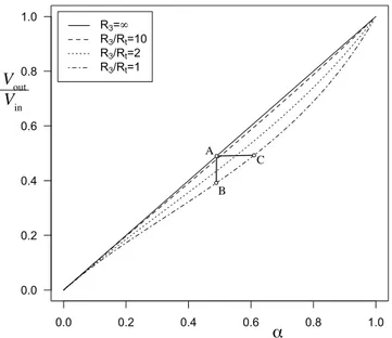
Figure 6 is a plot of Equation (17), withαon the horizontal axis andR3/Rtas the parameter.
The solid line corresponds toR3=∞, i.e., the simple potentiometer model where the load resistance
is so large that it is not important. For a givenα, points A and B shows the range ofVout/Vinwhen
R3 varies from∞to Rt. For a given, desired Vout/V in, the points A and C show thatαneeds to
change (the wiper needs to be moved) whenR3 is not large enough to be neglected.
The analysis in this section shows that the load resistance is not a big obstacle to using a potentiometer. The computations summarized in Table 1 demonstrate that with R3/R2 > 100,
the effect of the load resistance on the output voltag is negligible. Figure 6 shows that even when
R3/Rt = 1, the effect of the output resistor can be compensated by making a modest adjustment
to the potentiometer. We conclude that the simpler potentiometer formula, Equation (5), can be used for most engineering design calculations.
0.0 0.2 0.4 0.6 0.8 1.0 0.0
0.2 0.4 0.6 0.8
1.0 R
3=
R3/Rt=10
R3/Rt=2
R3/Rt=1
V
outV
inα
A
B C
+ –
R
1R
2V
outFigure 7: Using a voltage divider to supply variable voltage from a 9V battery.
3
Application: Using a 9V Battery to Supply 5V Power
Consider the circuit in Figure 7 in which a potentiometer is connected to a nine volt battery. By adjustment of the potentiometer, the circuit in Figure 7 allows a 9V battery to supply a voltage between 0 and 9V. It is not an efficient way to control the power voltage since power is dissipated in
R1with no useful gain. However, this is one simple situation where a potentiometercould be used.
Suppose you wanted to create a 5V power supply using the idea from Figure 7, but you wanted to use fixed resistors instead of a potentiometer. Neglecting the current to the load resistor, what values ofR1 andR2would give Vout= 5V if Vin= 9V?
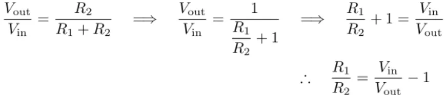
We begin the analysis by rearranging Equation (5). Solve forR1/R2:
Vout
Vin
= R2
R1+R2
=⇒ Vout
Vin
= 1
R1
R2
+ 1
=⇒ R1
R2
+ 1 = Vin
Vout
∴ RR1
2
= Vin
Vout
−1 (18)
Equation (18) allows us to find a ratio of resistors that will achieve a desired voltage output. For example, withVin= 9V andVout= 5V we obtain
Vin= 9V, Vout = 5V =⇒
R1
R2
= 9 5−1 =
4 5
What values of standard resistance satisfy the constraint R1
R2
= 4
5? Table 2 gives some standard values of 5% accurate resistors. Inspecting combinations of resistors shows that three possible combinations of resistors satisfy the requirement: R1 = 12 Ω and R2 = 15 Ω, or R1 = 16 Ω and
R2= 20 Ω, orR1= 24 Ω andR2= 30 Ω.
4
Summary
Table 3 shows the voltage divider schematics and output formulas for the two cases analyzed in Section 2. For most applications, we can safely use the simple formula obtained by assuming
Table 2: Standard resistor values for 5% accuracy. Resistors are mass produced at powers of 10 times the base values listed on the left. The values on the right are an example of the base values times 100. Seehttp://www.rfcafe.com/references/electrical/resistor-values.htm.
Base values Base values×100
10, 11, 12, 13, 15, 16, 18, 20, 22, 24, 27, 30, 33, 36, 39, 43, 47, 51, 56, 62, 68, 75, 82, 91
1000, 1100, 1200, 1300, 1500, 1600, 1800, 2000, 2200, 2400, 2700, 3000, 3300, 3600, 3900, 4300, 4700, 5100, 5600, 6200, 6800, 7500, 8200, 9100
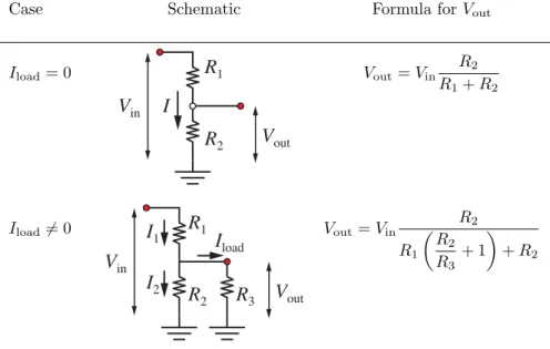
Table 3: Summary of voltage divider formulas. These formulas also apply when the two fixed resistors are replaced by potentiometer.
Case Schematic Formula forVout
Iload= 0
R
1R
2V
inV
outI
Vout=Vin
R2
R1+R2
Iload6= 0
R
1R
2R
3V
inI
1V
outI
2I
load Vout=VinR2
R1
R
2
R3
+ 1
5
Appendix A: Algebra to Simplify
1
−
R
1/R
effIn this section we will obtain a simplified form of the expression 1−R1/Reff that appears on the
right hand side of Equation (11). Start by working with the ratioR1Reff
R1
Reff
= R1
R1+
R2R3
R2+R3
= R1(R2+R3)
R1(R2+R3) +R2R3
=
R1
R
2
R3
+ 1
R1
R2
R3
+ 1
+R2
Now, subtract the preceding result from 1:
1− R1
Reff
= 1−
R1
R2
R3
+ 1
R1
R2
R3
+ 1
+R2
=
R1
R2
R3
+ 1
+R2−R1
R2
R3
+ 1
R1
R2
R3
+ 1
+R2
= R2
R1
R
2
R3
+ 1