Wavefrontshaping for absorption
optimization in a thin film silicon
solar cell.
THESIS
submitted in partial fulfillment of the requirements for the degree of
BACHELOR OF SCIENCE
in PHYSICS
Author : M.J. van Velzen
Student ID : 1046489
Supervisor : MSc. F. Mariani
Prof. Dr. M.P. van Exter 2ndcorrector : Dr. ir. S.J. van der Molen
Wavefrontshaping for absorption
optimization in a thin film silicon
solar cell.
M.J. van Velzen
Huygens-Kamerlingh Onnes Laboratory, Leiden University P.O. Box 9500, 2300 RA Leiden, The Netherlands
December 21, 2015
Abstract
Solar cells work by absorbing light to create electron - hole pairs and use a built-in electric field to separate these pairs to create a
current. We want to create a destructive interference for the reflected light of a thin film solar cell so that we increase the energy inside the solar cell. In our experiment we use a spatial light modulator to control the phase of the light wavefront that reaches the thin film solar cell. We have optimized the lightfront of a random phaseplate on the SLM with a partitioning algorithm.
This caused an 1.2% increase in the ratio between the current of the optimal phaseplate and a control phaseplate in only 4 iterations. After this the ratio became stable which indicates that
we created an optimal phaseplate. It is not yet clear if the increased current is caused by creating destructive interference for
Contents
1 Introduction 1
2 Theory 3
2.1 Solar cells 3
2.1.1 Carrier excitation 3
2.1.2 p-n junctions 4
2.1.3 Thin film solar cells 6
2.1.4 IV-curve 7
2.2 Shaping light to increase absorption 8
2.2.1 Destructive interference 9
3 Methods 11
3.1 setup 11
3.1.1 Controlling the wavefront 12
3.1.2 Imaging 12
3.1.3 Chopper & lock-in amplifier 13
3.1.4 Solar cell specifications 14
3.2 Superpixels & throughput 15
3.3 Algorithm to create the optimal phaseplate 16
4 Results & Discussion 17
4.1 Aligning 17
4.2 Power throughput after SLM 19
4.3 Measuring in the linear regime 20
4.4 Noise 23
4.5 Wavefront optimization 25
Chapter
1
Introduction
For many years the world has been trying to find replacements for fos-sil fuels. The reasons for this are numerous, like trying to combat global warming, being independent of the supply from other countries or prepar-ing for the inevitable when we run out. Many people seek a solution in re-newable energy from wind, the tides or most importantly for our research, the sun.
Solar cells are slowly becoming more common in society. They are a way to transform light into electrical energy and are clearly visible on a lot of buildings. Unfortunately there are not yet enough to fully replace fossil fuels. Their high initial cost and low efficiency make it a costly invest-ment. A lot of research has been going into making them more efficient or cheaper to produce. In our experiment we try to make the solar cell more efficient by changing the light instead of the solar cell.
Chapter
2
Theory
2.1
Solar cells
A solar cell transforms the energy from light into electricity. Because of the photovoltaic effect, the energy of incoming photons can raise the electrons inside the solar cell to a higher energy state. These higher energy electrons are then moved through an electrical circuit producing work.
2.1.1
Carrier excitation
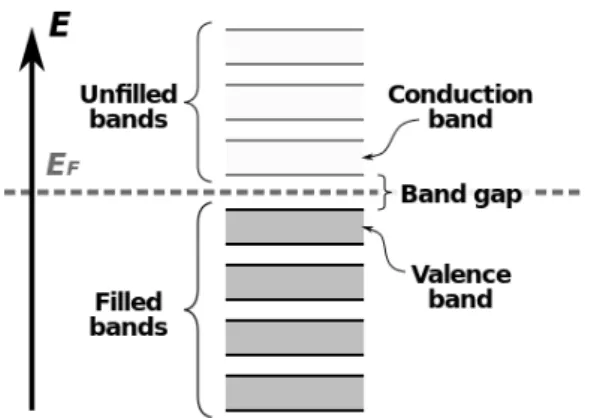
The majority of solar cells are made of semiconductors. Because of the Pauli exclusion principle the electrons of the semiconductor can not oc-cupy the same state and organize in bands of allowed levels. The highest accoupied band is called the valence band and is full of electrons. The band above it is empty in first approximation and is called the conduction band (fig 2.1).
The energy needed to excite an electron to the conduction band is de-pendent on the band gap, the energy difference of the conduction and the valence band. An incoming photon can be absorbed by a semiconductor and if the energy of the absorbed photon is equal or bigger than the band gap, the electron can be raised to the conduction band. Raising an elec-tron to the conduction band causes a hole to appear in the valence band. It is easiest to imagine this hole as a positively charged particle. Thus light falling on an semiconductor can create an electron in the conduction band and a hole in the valence band which are free to travel and transport charge and energy.
Figure 2.1: A Semiconductor electron band structure. The valence band is filled with electrons while the conduction band is empty.
conduct. It is possible to create a semiconductor which has more holes than free electrons or more free electrons than holes by introducing an im-purity in a process that is called doping. By placing an atom in the semi-conductor that has one more valence electron than the rest of the atoms this extra electron is not tightly bound by the crystal lattice. As a con-sequence free electrons are available in what is called n-type doping. By placing an atom in the semiconductor with one less valence electron the opposite type of doping can be obtained and is called p-type doping.
2.1.2
p-n junctions
Semiconductor solar cells use p-n junctions to stop the electron and hole from recombining. A p-n junction is established when a layer of p-type semiconductor and a layer of n-type semiconductor are brought together. In this situation free electrons from the n-type layer will diffuse to the p-doped region while the holes will diffuse to the n-p-doped region. The ex-cess electrons will fill the holes, essentially annihilating each other. This process leaves a depletion layer between the two regions where there are no free holes or electrons.
2.1 Solar cells 5
reaches an equilibrium and ends in a stable configuration with a built in electric field (figure 2.2).
Figure 2.2: In a p-n junction an n-doped region is in contact with a p-doped re-gion. Diffusion of the free electron and holes leave a depletion layer with a built in electric field. This electric field causes electron-hole pairs formed in the depletion layer to be split before they can recombine.
In a solar cell if a photon with enough energy is absorbed in the p-n junction it will raise an electron to the conduction band creating a hole and a free electron. If the electron-hole pair is formed within the depletion layer the electron will move to the n region and the hole to the p region under the effect of the built in electric field. This process is called the Pho-tovoltaic effect. In an open circuit these charges build-up and counteract the built in electric field. We can use the photovoltaic cell as a current generator by connecting its terminals to an external load.
2.1.3
Thin film solar cells
A thin film solar cell is a solar cell with mass-production possibilities. In contrast to silicon solar cells they are produced by physical or chemical deposition techniques which make them a cheaper but less efficient kind of solar cell [2].
A thin film solar cell consists of multiple layers. There are different structures possible but a possible construction is shown in figure 2.3. The first layer consists of glass which acts as a substrate for the solar cell. After that comes a layer of a Transparent Conductive Oxide (TCO) which is the front contact for our electrical circuit and must be transparent to let the light through. Then comes the semiconductor where the light is absorbed and the electron - hole pairs are seperated. The last layer is the back contact and is made of metal.
Figure 2.3: A schematic sketch of a thin film solar cell example from [3]. While the light is absorbed in the semiconductor the Transparent Conductive Oxide and the metal back reflector are neccesary for the contacts in an electrical circuit. The glass supports the solar cell mechanically.
Not every photon is absorbed by the semiconductor. The fraction of absorbed light is dependent on the thickness and properties of the material used. A thicker semiconductor absorbs more light because the photons have a higher chance excite an electron. We define the distance after which
the fraction 1
2.1 Solar cells 7
are typically wavelength dependent.
Another way to increase the absorbed light is to increase the path length of the light through the material. The metal back contact does this by re-flecting the light back into the semiconductor, doubling the path length.
In addition to this, the surface of the semiconductor is intentionally made rough. As seen in figure 2.3 a rough surface scatters the light, giving it multiple skewed trajectories. These give the light a longer path length and decrease the angle between the light and the back surface. Because of the decreased angle, the chance for internal reflection is increased, which makes it possible to trap light in the semiconductor [4].
2.1.4
IV-curve
You can plot the current generated by the solar cell against the voltage according to the formula
I = Io(eqV/kbT −1)−I
l (2.1)
Here Il is the photocurrent created by illuminating the solar cell and Io is the dark saturation current which is the current in the absence of light and created by diffusion in the solar cell. q is the elementary charge of an electron, V is the applied bias, kb is the Boltzmann constant and T is temperature in degrees Kelvin.
Figure 2.4 shows the IV-curve of a dark and an illuminated solar cell. In the dark a solar cell acts like a diode [2]. A reverse bias which creates a negative voltage hardly changes the current. A forward bias which creates a negative voltage increases the current exponentially.
The diode behaviour is caused by the depletion layer. A forward bias decreases the potential difference over the depletion layer. This makes the electric field weaker, making it easier for electrons to cross, and thins the depletion layer When the forward bias cancels the potential difference, the depletion layer is destroyed and the electrons are free to move, creating the exponential behaviour in the current.
A reverse bias increases the potential difference over the depletion layer. This strengthens the electric field and thickens the depletion layer. There-fore crossing the layer requires a higher energy and there will only be a small current. Only with an extensive reverse bias the solar cell will break down and allow a current increase quickly with the applied voltage [5].
Figure 2.4:The IV-curves show what happens to the current of a dark and illumi-nated solar cell when a voltage is applied. Ilis the current created by illuminating
the solar cell.
depletion layer are separated by the internal field in the depletion layer. When you plot the IV-curves for a dark solar cell and an illuminated solar cell you see that illuminating the cell essentially shifts the IV-curve down (figure 2.4). Applying a forward bias on an illuminated solar cell will thus first decrease the current until it reaches zero.
In our experiment we want to maximize Il without changing the power from the laser. To maximize Il we measure the current generated by the solar cell. With a stable temperature and voltage, the variations of Il lin-early affect the total current and we can thus find a maximum. To mea-sure variations in the total current we use a reverse bias. A reverse bias strengthens the field in the depletion layer which decreases the chance of an electron-hole pair recombining. A reverse bias thus increases the effi-ciency of charge carriers collection.
2.2
Shaping light to increase absorption
2.2 Shaping light to increase absorption 9
reflected light. A possible way to do this is by using interference.
2.2.1
Destructive interference
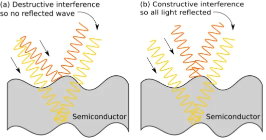
Light reaching the rough surface of the semiconductor is partially reflected and partially scattered inside the semiconductor. In the semiconductor the propagated light will be absorbed while it propagates. Some light will propagate through the semiconductor to eventually be scattered back into free space. Here the field will interfere with the field of the directly re-flected light. These fields are able to constructively or destructively inter-fere, strengthening or weakening the resulting field (figure 2.5).
Figure 2.5: Some light is reflected from the semiconductors front and back inter-face. The two reflected fields interfere in the free space. This results in a strength-ened or weakstrength-ened reflection and, more importantly, more or less light absorbed by the semiconductor.
Chapter
3
Methods
3.1
setup
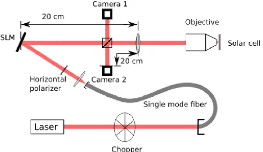
The setup we used for our experiment is shown in figure 3.1. We use a 4 mW helium-neon laser withλ= 632,8 nm and send light through a
chop-per and into a single mode fiber. After the single mode fiber a collimator creates a collimated beam and light is linearly polarized.
3.1.1
Controlling the wavefront
A Spatial Light Modulator (SLM) is a device that is able to spatially control the phase or intensity of light. The SLM we use consists of multiple pix-els of a translucent liquid crystal that has a controlled birefringent effect. This allows every pixel to adjust the phase of light falling on it. The device can be controlled via a computer to create different phaseplates and shape the wavefront reflected from the SLM. There are multiple possibilities for the use of an SLM like adaptive optics, speckle interferometry or seeing through scattering media [1]. Using the SLM to control the wavefront of the light falling on the solar cell, we want to make the reflected fields de-structively interfere in the free space.
The SLM works by changing its pixels refractive index and is optimized for linearly polarised light. We thus place horizontal polariser before the light reaches the SLM. After the SLM the light reaches a beamsplitter which sends 30% of the light intensity to camera 1. To focus the other 70% of the light intensity on the 4x4 mm solar cell we use an imaging system con-sisting of a lens and an infinity-corrected objective. Reflected light from the solar cell is sent back to the beamsplitter. The beamsplitter then sends light to camera 2 which is placed the same distance from the lens as our SLM.
To fully control the wavefront falling on the solar cell we need to know if our solar cell is in the focus of the objective. We can check this by using the conventional use of the objective as a microscope. If we shine some light on the solar cell while it is in the focus of the objective, it gives an image on camera 2. We use camera 1 to see if the phaseplate off the SLM is in the middle of our light beam.
3.1.2
Imaging
3.1 setup 13
Figure 3.2: Our imaging system consisting of a tube lens and objective focusses the light from the SLM on the solar cell.
3.1.3
Chopper & lock-in amplifier
We want to accurately measure only the photocurrent generated by the wavefront shaped light. All other light or sources of fluctuations are noise. A way to separate the signal from the noise is by using a chopper and a lock-in amplifier. The chopper is a small rotating fan which shapes the light excitation into square wave pulses.
3.1.4
Solar cell specifications
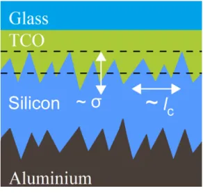
The solar cell we use in our experiment consists of an aluminium back reflector, an amorphous silicon p-i-n semiconductor, TCO and a glass sur-face. The silicon has a roughness ofσ= 40nm and lc = 200 nm whereσ is
the root mean square deviation of the height andlcis its lateral correlation lenght (figure 3.3).
Figure 3.3:Roughness of the solar cell.
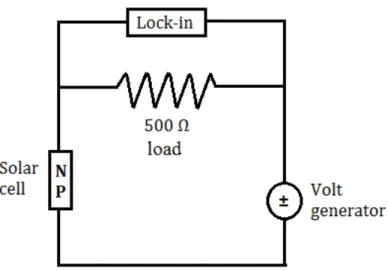
We measure the current from the solar cell according to the electronic circuit in figure 3.4. The volt generator is connected to the solar cell to supply a reverse bias of 0.5 V. The lock-in amplifier measures the voltage over the load resistor and sends it to the computer. We will use Ohm’s law
I = V
RL (3.1)
3.2 Superpixels & throughput 15
Figure 3.4: Our solar cell cell is in series connected with a volt generator and a
RL= 500Ωload. The lock-in amplifier is paralel connected to the load. This way
it can measure the voltage over the solar cell.
3.2
Superpixels & throughput
Light coming from different pixels must be distinguishable when it reaches the solar cell. We can calculate the size of the diffraction limited spot on the solar cell using the Abbe diffraction limit:
λ
2∗N A =d (3.2)
Here λ is the wavelength of our laser, NA is the numerical aperture of
our system and d is the maximum diameter of the spot we can image that is distinguishable. The NA of our system is determined by our objective which has an NA of 0.6 and we use a laser withλ=632, 8nm. The
diffrac-tion limited spot is thus 632, 8
2∗0.6 = 527nm. The pixels on the SLM have a diameter of 8µmand our imaging system has a 40 times de-magnification
3.3
Algorithm to create the optimal phaseplate
We need an algorithm that creates a phaseplate that forms the optimal wavefront for the light that reaches the solar cell.
To create this phaseplate we need an algorithm that has multiple iter-ations with a feedback loop. In these iteriter-ations pixel(s) cycle from 0 to 2π
in n steps and at the end the optimum phaseplate is chosen. There are multiple algorithms that do this like sequential algorithms that cycle only one pixel or partitioning algorithms that cycle multiple pixels [7].
Chapter
4
Results & Discussion
4.1
Aligning
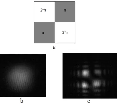
To be able to increase the current from our solar cell we need to have con-trol of the wavefront that reaches the cell. This means that our setup must be fully aligned and the laser spot on the SLM must be fully encompassed by the phase plate. The easiest way to ensure that the laserspot is encom-passed is to have the center of the phase plate in the center of the laser spot. We use the aligning phase plate shown in figure 4.1 to test this. When the center of the phase plate is in the center of the laser spot we see a certain symmetric light spot on camera 1.
Figure 4.1: Procedure used to align the SLM (a) The aligning phaseplate on the SLM. (b) A picture from camera 1 of the laserspot without an phaseplate on the SLM. (c) A picture from camera 1 with the aligning phaseplate on the SLM. The symmetric lightspot means the center of the phaseplate is on the center of the laserspot.
4.2 Power throughput after SLM 19
4.2
Power throughput after SLM
The SLM is not a perfect device, it has a fill factor of 93%. Because we can not control 7% of the SLM even a flat phaseplate creates an diffraction pat-tern. Only the center spot of this diffraction pattern falls in our throughput which leaves us with 60% of the lightpower.
Random phaseplates on the SLM can change the power throughput by diffracting light outside of our optics. We use a photodiode to measure the throughput dependance on the size of our superpixels. We first performed a calibration curve of the photodiode (figure 4.3). By fitting the results we can now use the output of the photodiode to calculate the power of the light.
Figure 4.3:A calibration of the photodiode shows that its voltage output changes linearly with the power on the photodiode.
By replacing the solar cell with the photodiode, we measure the power throughput of 10 different random phaseplates for superpixel sizes rang-ing from 1 to 20. Figure 4.4 shows the average power reachrang-ing the photodi-ode for every superpixel size. Pixelsize of zero corresponds to a flat phase-plate. This has the maximum throughput and we use this to normalize our results. It is clear that small superpixel sizes cause less power througput and that bigger superpixels slowly converge to the reference point. For our experiment we use a superpixel size of 4. This leaves 66% of the
through-put from a flat phaseplate. This leaves us with 66%∗60%
Figure 4.4:The superpixels diffraction reduces the throughput of our optical sys-tem: Smaller superpixel sizes causes more light loss while bigger superpixels slowly converge to the maximum of a flat phaseplate.
4.3
Measuring in the linear regime
We want the photocurrent to be proportional to the absorbed light, so we need to check if the solar cell has a linear response to lightpower. To find this linear regime we will look at multiple IV-curves.
Looking at the IV-curves of our solar cells we noticed they deteriorated over time, sometime assuming the shape expected for resistive behaviour. This means that we somehow broke our solar cells (figure 4.6). To explain the reason our cells broke we looked at multiple causes including our bias source. After measuring the output of the bias source (figure 4.5) we found that peak voltages appeared when we turned the bias source on or off. We obtained stable IV-curves when we made sure that the solar cell was never connected to the bias source when this was switched on/off.
4.3 Measuring in the linear regime 21
Figure 4.5: A voltage measurement of our bias source. (1) The bias source is turned on. (2) The output of the bias source is turned on. (3) The bias source is set to a 1 V output. (4) The bias source is turned off.
Figure 4.7: IV-curves of the cell we used with different laserpowers on the cell. With more power on the cell the lines shift downwards according to the formula [2.1]. That there is a current for a reverse bias without light indicates that the solar cell used has a greater than normal dark saturation current (.
4.4 Noise 23
4.4
Noise
To be able to use our algorithm, the increase of the output of the solar cell must be bigger than the noise in our system. To find the noise in our sys-tem we first measured the light power of our laser for 100 seconds with a powermeter (figure 4.9). With the laser [70,2 mA] we measured an average of 55.6µW. The signal has a standard deviation of 0.0338µW which gives
us a signal to noise ratio of 0.06%.
Figure 4.9: The fluctuations of the laser output measured with a powermeter on the spot of the solar cell.
With the laser focused on the solar cell we measured its output for 30 seconds using the lock-in (figure 4.10). The average current from the solar cell is 4.841 µA with a standard deviation of 0.005 µA which gives us a
signal to noise ratio in our whole system of 0.11%. This is the threshold for noticeable changes in our system.
Figure 4.10: The output of the solar cell over 30 seconds. The measurement is made with a lock-in amplifier while a constant lightpower of 76µW falls on the
cell.
Figure 4.11: The output of the solar cell over 20 minutes. Every 30 seconds a measurement is made. After 90 seconds the laser is turned on with a constant output and 142µW reaching the cell. At the end of the measurement the current
4.5 Wavefront optimization 25
4.5
Wavefront optimization
Figure 4.12 shows the measured current for every step in multiple itera-tions. The iterations show a waveform with a clear minimum and maxi-mum. Iteration 1 has a maximum at 70.9µAand a minimum at 69.8µA.
The variance in the iteration is 1,6% of the average output which is a fac-tor of 10 bigger than the signal to noise ratio in our system. This shows that the modulation is an effect of the projected phaseplate. The difference between the average output of iteration 1 and 5 is twice as big as the dif-ference between the average of iteration 10 and 15. This indicates that the output is converging to a maximum.
Figure 4.12: In every iteration half of the pixels are cycled from 0 to 2π in 10
steps. The plot shows the measured voltage output of the solar cell for every step in iteration 1, 5, 10 and 15. The four iterations have a sinusoidal fit and all show a clear maximum.
Figure 4.13 shows the output of the solar cell after every iteration for a flat and optimized phaseplate and their ratio. The output for the flat phaseplate is used as a control signal to monitor fluctuations of the laser and the solar cell.
4.5 Wavefront optimization 27
Chapter
5
Conclusion
In our set-up we control the wavefront of the light that reaches our thin film solar cell. We have shown that using the partitioning algorithm it is possible to optimize a random phaseplate to increase the output of a solar cell. We have shown that we are in the linear regime of our solar cell where an increased output is directly correlated to the increased light power on the solar cell and that the increase in the ratio by 1.2% is bigger than the noise in our system. The sinusoidal waveform that is visible in every iteration of our algorithm is an indication that there is an optimal phaseplate.
References
[1] A. P. Mosk, A. Lagendijk, G. Lerosey, and M. Fink,Controlling waves in space and time for imaging and focusing in complex media, Nature Photon-ics6, 283 (2012).
[2] J. Nelson, The Physics of Solar Cells, Series on Properties of Semicon-ductor Materials, Imperial College Press, 2003.
[3] U. Palanchoke, V. Jovanov, H. Kurz, P. Obermeyer, H. Stiebig, and D. Knipp,Plasmonic effects in amorphous silicon thin film solar cells with metal back contacts, Optics Express20, 6340 (2012).
[4] O. Isabella, J. Krˇc, and M. Zeman,Modulated surface textures for enhanced light trapping in thin-film silicon solar cells, Applied Physics Letters97, 101106 (2010).
[5] O. Breitenstein, J. Bauer, K. Bothe, W. Kwapil, D. Lausch, U. Rau, J. Schmidt, M. Schneemann, M. C. Schubert, J.-M. Wagner, and W. Warta,Understanding junction breakdown in multicrystalline solar cells, Journal of Applied Physics109, 071101 (2011).
[6] P. A. Temple,An introduction to phasesensitive amplifiers: An inexpensive student instrument, American Journal of Physics43, 801 (1975).

![Figure 2.3: A schematic sketch of a thin film solar cell example from [3]. While the light is absorbed in the semiconductor the Transparent Conductive Oxide and the metal back reflector are neccesary for the contacts in an electrical circuit](https://thumb-us.123doks.com/thumbv2/123dok_us/8319670.2204945/12.892.392.558.514.811/schematic-semiconductor-transparent-conductive-reflector-neccesary-contacts-electrical.webp)