Pb-Free High Temperature Solder Joints for Power Semiconductor
Devices
Yasushi Yamada*, Yoshikazu Takaku**, Yuji Yagi*, Ikuo Nakagawa***, Takashi Atsumi***, Mikio Shirai***, Ikuo Ohnuma** and Kiyohito Ishida**
*Toyota Central R&D Labs.,Inc., 41-1, Yokomichi, Nagakute, Nagakute-cho, Aichi 480-1192, Japan
**Tohoku University, Aoba-yama 6-6-2, Sendai-city, Miyagi 980-8579, Japan
***Toyota Motor Corporation, 1 Toyota-cho, Toyota-city, Aichi 471-8572, Japan (Received August 4, 2009; accepted November 2, 2009)
Abstract
Three types of inexpensive Pb-free solder joints, namely Zn-based and Bi-based solders, and a CuSn alloy were studied for application to the high-temperature operation of wide band-gap power semiconductor devices using GaN or SiC. Zn– Al solder sheets, whose melting point is 380°C were prepared, and then surface oxides were removed by RF plasma etching. Subsequently, Cu thin films were deposited by the DC sputtering method on the solder sheet. After that, joint samples were fabricated using a conventional electrical furnace with H2/N2 gas flow. That the joints were sufficiently dense was confirmed by scanning acoustic microscope. The wettability of the solder was improved due to contact between the pure Zn–Al solder without oxide and the Ni surface of the substrate, and the chemical reaction between the Zn–Al solder and the deposited Cu thin film. Bi with CuAlMn particle solders, whose melting point is 270°C, were fab-ricated and it was found that the solder has almost double the tensile strength of pure Bi. Excellent wettability was observed with the Ni or Pd thin film deposited on the Cu substrate. It was found that deposited Ni or Pd was not observed in the interface between the substrates after the joint samples were fabricated. CuSn alloy joints were fabricated using Sn thin films deposited and annealed on Cu substrates. The temperature during the annealing was kept at approximately 350°C; therefore, only the Sn film was melted and some chemical reaction occurred between the liquid Sn and solid Cu. Then, Cu3Sn alloy, whose melting point is 640°C, appeared in the joint and the composition was confirmed by X-ray dif-fraction analysis. Furthermore, it was found that the CuSn alloy is harder than Cu as measured by nano indentation analysis. In addition, the joints showed excellent thermal cycle reliability.
Finally, the properties of these joints are summarized.
Keywords:Solder, Joint, Pb-free, Power Semiconductor, Reliability
1. Introduction
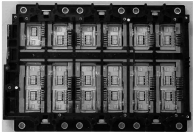
Electrical vehicles such as hybrid electrical vehicles are set to play a role in reducing the carbon dioxide exhausted from automobiles. These vehicles use electrical inverters that convert from DC to three-phase AC. Many power semiconductor devices are used for the inverters and are mounted on substrates as shown in Fig. 1.[1] The invert-ers are required for small size; therefore, high power den-sity is required as shown in Fig. 2.[2]
Considering the miniaturization of the inverters, the high-temperature operation of the devices is an important challenge. Next generation power devices using GaN and SiC are applicable for such high temperature operations, exceeding 200°C, and the packaging technologies, such as
joint materials and processes, should be studied.
Sn-based lead-free solders are well-known materials. However, their melting points are around 220°C, which is not sufficient for the high temperature operation of power devices. Novel metal-based materials such as Au–Sn sol-ders and sintered Ag joints are expensive, so they are dif-ficult to use for automobiles.
In this paper, three new types of solder joints, including a Zn-base solder, a Bi-base solder and a CuSn alloy joint are described.
2. Zn-base Solder Joint
A eutectic Zn–Al solder has a melting point of 380°C[3] and it can be formed as a sheet. However, the surface
oxides of the solder are difficult to remove under the reductive atmosphere around 300 to 400°C. Furthermore, even if the oxides are removed mechanically, new oxides quickly appear in air.
For these reasons, the surfaces of the solder sheets were removed by RF plasma etching; subsequently, Cu thin films of 50 nm thicknesses were deposited by the DC sputtering method without a vacuum break. A photo of the sample is shown in Fig. 3. The sample before those pro-cesses, shown in Fig. 3, is covered with native oxide on the solder surface. On the other hand, after those processes, the sample is covered with Cu thin film. In addition, it was found that the thin film of Cu on the substrate enhanced the wettability due to the chemical reaction between the Zn and Cu.
The joint samples were fabricated using a conventional electrical furnace with 5%H2/N2 gas flow at 430°C for 30 minutes. Then the samples were observed with a SAM (Scanning Acoustic Microscope) as shown in Fig. 4. The joint sample without the wettability improvement men-tioned above shows white parts around the edge of the sample. Those parts seem to be voids or cracks. On the other hand, the joint sample with the mentioned improve-ment looks almost black, so it seems that the joint is
suffi-ciently dense.
In addition, a cross-sectional photo of the joint sample made with a SEM (Scanning Electron Microscope) is shown in Fig. 5. Few voids and cracks are found in the solder layer and at the interface between the solder and substrates as well. Therefore, it seems that this joint is suf-ficiently dense for the power device packaging.
3. Bi-based Solder Joint
Bi is a metal whose melting point is 270°C. However, it is brittle and has low tensile strength. To overcome these inferior properties, a new Bi-based solder with CuAlMn particles was fabricated because the melting temperature is controlled by the Bi-based matrix and relaxation of ther-mal stress is expected due to the martensite transforma-tion by CuAlMn particles.[4]
The composition of the particle was designed as Cu– Fig. 1 A power module used in hybrid vehicle.
Fig. 2 Power density increase of electrical converters.
(a) Before the wettability improvement process
(b) After the wettablity improvement process Fig. 3 Photo of Zn-based solder sheet.
(a) Without the wettability improvement process
(b) With the wettability improvement process Fig. 4 SAM observation of joint sample.
23at%Al–2at%Mn in order to obtain the solder layer of 60:30:10 of Bi:CuAlMn:Bi3Ni. The CuAlMn particles were prepared by gas-atomizing method. After that, each parti-cle was coated with electroless Ni plating using a dropping method to improve Bi wettability on the particles. Then the coated particles were mixed with Bi melt and ingots of the solder were obtained. The cross-sectional microstructure is shown in Fig. 6.
Specimens for the mechanical property test were pre-pared from the cast ingots. They were almost 10 mm in diameter and 60 mm in length. The specimens were machined using an electric-discharge machining method and were annealed at 50°C for 30 minutes to remove the stress induced by the machining.
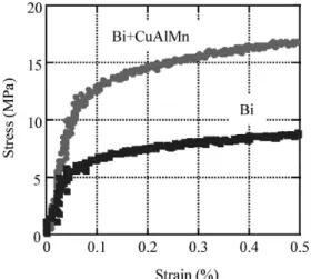
The stress-strain properties of the fabricated specimen are shown in Fig. 7. It was found that the tensile strength of the fabricated solders was remarkably improved in com-parison with that of pure Bi. In addition, the mechanical properties strongly depend on the temperature, as shown in Fig. 8. The fracture strains were very small at –40°C and
25°C and are brittle-like. On the other hand, large strains were found at 105°C and 195°C. In addition, the tensile strength remained around 10MPa at 195°C; therefore, it seems that the solder itself has sufficient strength at around 200°C.
Bi itself has poor wettability on substrates, so thin films of other metals deposited on the Cu substrates were exam-ined to overcome the problem. Small pellets of Bi were
Fig. 6 Cross sectional microstructure of Bi + CuAlMn solder.
Fig. 7 Stress and strain curve of the Bi-based solders.
Fig. 8 Temperature dependency of stress and strain proper-ties of Bi+CuAlMn solder.
Fig. 9 Wettability test result of Bi solder for different surface finished on Cu substrate.
Fig. 10 Cross section observation of wettability test sample of Pd deposited substrate.
melted in a 5%H2/N2 gas flow using an electrical furnace. Photos of the Au, Ni or Pd deposited on the Cu substrates after melting tests are shown in Fig. 9. The areas of the sol-der spreading with the Ni or Pd deposited samples are larger than that of the Au deposited sample. Generally, Au thin film is used to improve the wettability; however, excel-lent wettability is observed with 50nm of Ni or Pd thin film deposited on the Cu substrate. The chemical interaction between Bi and deposited Ni or Pd seems to be very high. In addition, the deposited Ni or Pd was not observed at the interface after the Bi was melted on the substrate as shown in Fig. 10. Therefore, the deposited materials seem to be diffused in the melted solder.
4. CuSn Alloy Joint
CuSn alloys such as Cu3Sn and Cu6Sn5 have high melt-ing points, 640°C and 415°C, respectively. Therefore, if the devices are heated beyond those melting points, the devices might be damaged. On the other hand, Sn and Cu are known to show high chemical reactivity even when solid. Accordingly, CuSn alloy joints were fabricated with Sn films 2 or 10 μm thick deposited and annealed on both sides of Cu substrates. The annealing was carried out at 350°C for 30 minutes in a 5%H2/N2 gas flow with 5 MPa screw pressure. Therefore, only the Sn was melted and a chemical reaction occurred between liquid Sn and solid Cu.
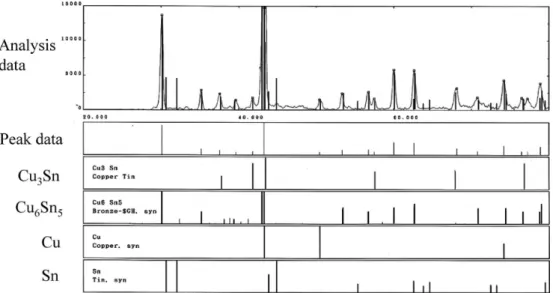
After the annealing process, CuSn alloys are found between the Cu substrates as shown in Fig. 11. A single material is observed for the 2 μm Sn film sample, while two materials are found with the 10 μm film Sn sample. The cross-section of the 10 μm joint was analyzed by X-ray
dif-fraction analysis. Peaks of Cu3Sn and Cu6Sn5 were detected. However, no peaks of single phase Sn were detected in the joint, as shown in Fig. 12. All of the depos-ited Sn film seems to have reacted with the Cu substrate and changed to CuSn alloys. This indicates that those CuSn alloy joints will show high-temperature durability,
(a) Sn thin film: 2 μm
(b) Sn thin film: 10 μm Sn
Fig. 11 Cross sectional microstructure of CuSn alloy joint.
even above the melting point of Sn.
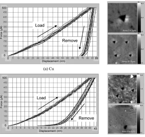
Furthermore, nano indentation analysis was carried out to measure the hardness of the CuSn alloy. A maximum 500 μN force at the rate of 100 μN/s was applied to the joint, and the displacements were measured several times. Almost 86 nm of the maximum displacement was mea-sured for Cu. On the other hand, 42nm was meamea-sured for Cu3Sn, as shown in Fig. 13. The calculated Young's modu-lus are 118 GPa for Cu and 146 GPa for Cu3Sn. Photos in Fig. 13 show the pressed marks of the probe. It is observed that the areas of the marks for Cu are larger than
those of Cu3Sn. Consequently, it is seen that the Cu3Sn alloy are harder than Cu.
Additionally, those joint showed almost no damage after the wide temperature range of a thermal cycle test such as 2000 cycles of –40/230°C. From these results, the joint seems to have excellent reliability.
5. Conclusion
Three types of inexpensive, Pb-free solder joints, namely a Zn-based solder, a Bi-based solder, and a CuSn alloy were studied for the high-temperature operation of wide Fig. 13 Comparison in hardness using nano indentation analysis (Rate: 100 μN/s, Lines: repeat, Right photo: pressed mark).
Table 1 Properties of joints.
Properties Zn–Al Bi + CuAlMn Cu3Sn Mechanical Strength (R.T.) 150 MPa 15 MPa > Cu
Thermal conductivity High
(Zn: 117W/mK) Low
(Bi: 8W/mK)
Moderate Electrical Conductivity High
(Zn: 5.5 μΩcm) Low
(Bi: 107 μΩcm)
Moderate Chemical Melting point 380°C 270°C 640°C
(process 350°C) Suggested interface Ni with Cu thin
film
Cu with Ni or Pd thin film
band-gap power semiconductor devices. Considerable functionality was obtained using several approaches to overcome the technical difficulties. The important proper-ties of these joints are summarized in Table 1. Zn-based solder has superior mechanical and electrical properties and is suggested for conventional Ni plating surfaces. Bi-based solders show relatively lower mechanical and electrical properties; therefore, it might be applicable to relatively low heat flux regions such as around heat sinks. CuSn alloy joints have moderate mechanical and electrical properties. However, they are limited to thin joints on the order of μm size. Generally, more than two kinds of joints are used for power modules, so appropriate joints can be applied in the design of the power module.
References
[1] T. Kojima, Y. Yamada, Y. Nishibe, M. Ciappa and W. Fichtner, “A Novel Compact Thermal Modeling
Approach to Electro-thermal Simulation for Automo-tive IGBT Modules”, Proc. of IPEC-Niigata, pp. 787– 792, 2005.
[2] H. Ohashi, I. Omura, S. Matsumoto, Y. Sato, H. Tadano and I. Ishii, “Power Electronics Innovation with Next Generation Advanced Power Devices”, IEICE, Vol. E87-B, No. 12, pp. 3422–3429, 2004. [3] Y. Yamada, Y. Takaku, Y. Yagi, I. Nakagawa, T.
Atsumi, M. Shirai, I. Ohnuma and K. Ishida, “Relia-bility of wire-bonding and solder joint for high temper-ature operation of power semiconductor devices”, Microelectronics Reliability, Vol. 47, pp. 2147–2151, 2007.
[4] Y. Takaku, I. Ohnuma, Y, Yamada, Y. Yagi, Y. Nishibe, Y. Sutou, R. Kainuma and K. Ishida, “Bi-Base Compos-ite Solders for Mounting Power Semiconductor Devices”, JIEP, Vol. 11, pp. 141–146, 2008.