Electron Diffraction and Microscopy Study of Nanotubes and
Nanowires
Hakan Deniz
A dissertation submitted to the faculty of the University of North Carolina at Chapel Hill in partial fulfillment of the requirements for the degree of Doctor of Philosophy in the Department of Physics and Astronomy.
Chapel Hill 2007
Approved by:
Advisor: Professor Lu-Chang Qin
Reader: Professor Hugon Karwowski
Reader: Professor Rene Lopez
Reader: Professor Laurie McNeil
Reader: Professor Sean Washburn
©2007
Hakan Deniz
iii
ABSTRACT
HAKAN DENIZ: Electron Diffraction and Microscopy Study of Nanotubes and
Nanowires
(Under the direction of Dr. Lu-Chang Qin)
Carbon nanotubes have many excellent properties that are strongly influenced by their
atomic structure. The realization of the ultimate potential of carbon nanotubes in
technological applications necessitates a precise control of the structure of as-grown
nanotubes as well as the identification of their atomic structures. Transmission electron
microscopy (TEM) is a technique that can deliver this by combining the high resolution
imaging and electron diffraction simultaneously. In this study, a new catalyst system (the
Co/Si) was investigated in the production of single-walled carbon nanotubes (SWNTs) by
laser ablation. It was discovered that the Co/Si mixture as a catalyst was as successful as
the Ni/Co in the synthesis of SWNTs. The isolated individual SWNTs were examined by
using nanobeam electron diffraction for the structure identification and it was found that
carbon nanotubes grown by this catalyst mixture tend to be slightly more metallic.
The electron diffraction technique has been refined to establish a new methodology to
determine the chirality of each shell in a carbon nanotube and it has been applied to
determine the atomic structure of double-walled carbon nanotubes (DWNT), few-walled
carbon nanotubes (FWNT) and multi-walled carbon nanotubes (MWNT). We observed
Several FWNTs and MWNTs have been examined by our new electron diffraction
method to determine their atomic structures and to test the efficiency and the reliability of
this method for structure identification. We now suggest that a carbon nanotube of up to
25 shells can be studied and the chirality of each shell can be identified by this new
technique. The guidelines for the automation of such procedure have been laid down and
explained in this work.
The atomic structure of tungsten disulfide (WS2) nanotubes was studied by using the
methods developed for the structure determination of carbon nanotubes. The WS2
nanotubes are another example of the tube forming ability of the layered structures and a
member of the family of inorganic fullerene-like structures. These nanotubes are much
larger in diameter than carbon nanotubes. The tubes studied here have helicities less than
18o and usually have near zigzag structure.
The short-range order (SRO) in the atomic structure of carbon soot produced by laser
ablation was investigated using electron diffraction and radial distribution function (RDF)
analysis. The effects of the furnace temperature and the metal catalyst on the SRO in the
carbon soot were also studied. It was discovered that the SRO structure is the same for all
carbon soot samples studied and is very similar to that of amorphous carbon. These
techniques were also applied to determine the atomic structure of amorphous boron
nanowires. We found out that the atomic structure of these boron nanowires agree well
v
ACKNOWLEDGEMENTS
I would like to extend my sincere gratitude and thanks to my advisor Lu-Chang Qin
who has supported me, guided me and encouraged me in my research and in my struggles
over last three years here making it possible for me to finish this work. I would like to
express my special thanks to Qi Zhang from whom I have learned a lot of information
about operation and application of transmission electron microscopy. I also would like to
thank my previous and current group members, Zejian Liu, Gongpu Zhao, Han Zhang,
Letian Lin who were always kind and helpful to me in my research and my life in the
group. I especially want to thank my friend Anna Derbakova by making my life easier in
my research with computer scripts that she wrote.
I would like to give my thanks to Dr. Otto Zhou who was so nice in letting me use his
laser ablation system and his laboratory extensively for my research. I also would like to
thank my entire committee members, Dr. Hugon Karwowski, Dr. Laurie McNeil, Dr.
Rene Lopez, and Dr. Sean Washburn for their guidance and encouragement. Finally, I
would like to thank my best friends Shon Gilliam and Ted Uyeno for their friendship, for
TABLE OF CONTENTS
Chapter
1. Introduction……….1
1.1 Structural Order and Disorder………...1
1.2 Carbon Nanotubes (CNT)……….4
1.2.1 Structure……….4
1.2.2 Electronic Properties………..7
1.3 CNT Characterization Techniques...………...12
1.3.1 Scanning Tunneling Microscopy (STM)……….12
1.3.2 Raman Spectroscopy………14
1.3.3 Optical Absorption Spectroscopy………...15
1.4 Inorganic Nanotubes………...16
1.5 Objectives………...18
1.6 References………...20
2. Theory of Electron Diffraction and Imaging for Carbon Nanotubes…………....24
2.1 Theory of Diffraction………..24
2.2 Imaging of CNT by TEM………...30
vii
2.3 References………...42
3. Characterization of SWNTs Produced by Laser Ablation of Si Containing Catalysts……….44
3.1 Synthesis of CNTs………..44
3.2 Production of SWNTs by Laser Ablation……...47
3.3 TEM and NBED Characterization………..…48
3.4 Analysis of SWNTs Produced by Si Containing Catalysts………55
3.5 Summary and Conclusions……….62
3.6 References………...65
4. Structure Characterization of MWNTs……….69
4.1 Characterization of DWNTs………...70
4.2 Characterization of FWNTs………85
4.3 Characterization of MWNTs………...99
4.3.1 Introduction………..99
4.3.2 Application of Indexing Method………106
4.4 Summary and Conclusions………...124
4.5 References……….129
5. Tungsten Disulfide (WS2) Nanotubes……….133
5.1 Introduction………...133
5.2 Structure………135
5.3 TEM and NBED Characterization of WS2 Nanotubes……….138
5.4 Summary and Conclusions………...154
5.5 References……….…159
6.1 Introduction and Motivation……….162
6.2 Amorphous Carbon Soot………..163
6.3 Electron Diffraction and RDF Analysis of Soot………...167
6.3.1 Theoretical Background……….167
6.3.2 RDF of Carbon Soot………..169
6.4 Fluctuation Electron Microscopy (FEM) on Carbon Soot………175
6.4.1 Theory and Overview………...175
6.4.2 Experimentation and Results………...181
6.5 Boron and Its Structure……….183
6.6 Amorphous Boron Nanowires………..186
6.7 RDF Analysis of Amorphous Boron Nanowires………..190
6.8 Summary and Conclusions………...195
6.9 References……….199
7. Summary and Conclusions……….202
Appendix A. Table for Chiral Indices of DWNTs………....209
Appendix B. Tables for Chiral Indices of FWNTs………...210
ix
ABBREVIATIONS
CNT Carbon nanotube
CRN Continuous random network
DWNT Double-walled carbon nanotube
FEM Fluctuation electron microscopy
FWNT Few-walled carbon nanotube
HRTEM High-resolution transmission electron microscopy
MRO Medium-range order
MWNT Multi-walled carbon nanotube
NBED Nano-beam electron diffraction
RDF Radial distribution function
RRS Resonant Raman spectroscopy
SRO Short-range order
STM Scanning tunneling microscopy
SWNT Single-walled carbon nanotube
Chapter 1
Introduction
Since its invention in 1932, transmission electron microscopy (TEM) has been a major
tool for researchers to study the structure of materials from crystalline to amorphous. It
has been in use for imaging, diffraction and chemical analysis of solids. Traditionally,
x-ray or neutron diffraction has been the principal method for the study of crystals while
TEM has been used to image individual atoms and to study defects in crystals. TEM has
now become an indispensable technique for research in the field of nanotechnology in the
last decade especially after the observation of carbon nanotubes was first carried out in a
TEM [1].
1.1 Structural Order and Disorder
The atomic structure of materials can be grouped in three major categories: short-range
order (SRO), medium-range order (MRO) and long-range order (LRO). The long range
order refers to the crystalline form of matter. The structure of perfect crystals is relatively
easy to describe because they follow translational periodicity and symmetry.
SRO and MRO
2
structure can only be defined in terms of a unit cell with an infinite number of atoms.
Therefore, a statistical description of the structure is inevitable. Although there is no long
range order in amorphous materials, there is a very well defined short-range order since
two atoms can not approach each other closer than a typical bond length. So, the atomic
structure can be described in terms of a pair density function that gives the probability of
finding an atom at a distance r from an average atom excluding itself. The atomic
structure can be obtained statistically through the radial distribution function (RDF)
constructed from experimentally measured scattering intensities. The RDF curves show a
very sharp first peak corresponding to the nearest inter-atomic distance in the sample and
the successive peaks following it with broadened widths. It only gives the information
about a single structural unit and its immediate connection to the next neighbors and
fades away very quickly, making it difficult to obtain any kind of structural information
beyond the length scale of ~0.8 nm [2-4]. Since the RDF analysis gives information about
the average structure of the material, the three-dimensional atomic structure can never be
determined unambiguously.
The continuous random network (CRN) model was introduced in early 1930s to
explain the structure of covalently bonded glasses [5]. In the CRN model, the basic
structural unit of the glass is similar to that of its crystalline counterpart. For example, the
structural unit for vitreous SiO2 is a SiO4 tetrahedron. In the SiO4 tetrahedron, each Si
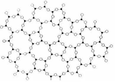
atom is bonded to four oxygen atoms and each oxygen atom to two Si atoms (Fig. 1.1.1).
The connections of the tetrahedra lead to a network structure in three dimensions with no
translational symmetry, in contrast to the structure of crystalline quartz. The complete
the coordination numbers of the structural unit and the distribution of the bond angles and
lengths. The medium-range order is the next structural length scale in glasses and
amorphous materials. It refers to the way that the basic units connect to each other to
describe a structure on the length scale up to 2 nm [6]. For the SiO2 case, the tetrahedra
are connected to each other through the corners with a random distribution of torsion
angles, and this leads to the structure (CRN) with almost non-existent medium range
order. The deviations from the corner sharing basic units, such as edge or face sharing
tetrahedra are an indication of an order higher than that of the short-range.
Fig. 1.1.1 Two dimensional schematic representation of the CRN model for SiO2 (black
dots for Si atoms and open circles for oxygen atoms). Adapted from reference [5].
Although the CRN model is successful in explaining the short range order and other
basic features of the network glasses, it fails to elucidate other properties such as mass
4
scattering vector values, meaning that it corresponds to larger distances in real space
beyond that of the short-range order. It is anomalous in the way that the real space
correlation function remains almost unchanged whether or not the FSDP is included in
the Fourier transform of the structure factor [7].
1.2 Carbon Nanotubes (CNT)
Carbon nanotubes have drawn an enormous amount of interest in the scientific
community since their discovery by Iijima in 1991 [1]. This novel form of carbon has
many extraordinary properties due to their nanometer-size diameter, large aspect ratio
and hollow core [8-11]. They are envisaged to have promising applications in areas
ranging from atomic probes, sensors, drug delivery systems, and transistors to flat panel
displays and electron field emitters. The properties of carbon nanotubes are very sensitive
to the geometry of their atomic structures [12-16] and the realization of the above
mentioned technological applications of carbon nanotubes requires precise control and
knowledge of their atomic structure.
1.2.1 Structure
A single-walled carbon nanotube (SWNT) can be obtained by rolling up a graphene
about an axis perpendicular to the chiral vector (perimeter vector) Ch
r
to make a seamless
hollow cylinder. The chiral vector is defined in terms of the primitive vectors of the
hexagonal graphene lattice by:
Ch uar1 var2
r
+
= , (1.2.1)
The angle between the basis vector ar1 and the chiral vector is called the chiral angle
(helical angle) or the helicity of the nanotube and is given by
] ) 2 ( 3 arctan[ u v v + =
α
. (1.2.2)The diameter d of the tubule is given by Ch/π where Ch is the circumference of the tube
and can be expressed as
d =Ch /π = Ch /π =a0 u2 +v2 +uv/π r
, (1.2.3)
in terms of the chiral indices and the lattice parameter a0 of the two dimensional
graphene (0.246 nm). Carbon nanotubes come in two different classes of symmetry:
chiral (helical) and achiral (non-helical) nanotubes. For chiral nanotubes, the chiral angle
lies in the range of [0o, 30o] if the handedness of the tubes is ignored (u ≥ v ≥ 0). For achiral nanotubes, there are two special cases. One is called the zigzag nanotube with
chiral indices of (u, 0) having the chirality of 0o. The other is called the armchair nanotube with chiral indices of (u, u) having the chiral angle 30o.
The periodicity of the nanotube is given by the translational vector T
r
which runs
parallel to the tube axis and perpendicular to the chiral vector Ch
r
. Together they define
the unit cell of the nanotube, also called the radial projection net. The translation vector
T
r
can be written using the basis vectors as
T utar1 vtar2
r
+
= (1.2.4)
where ut and vt are integers. Using the orthogonality relation between the chiral and
6
M v u
ut =− +2 , (1.2.5)
and
M v u
vt = 2 + , (1.2.6)
where M is the greatest common divisor of (2u+v) and (u+2v). Then the periodicity
of the tube takes the form of:
T = 3a0 u2 +v2 +uv/M = 3Ch/M
r
. (1.2.7)
Fig. 1.2.1 The unrolled graphene lattice of a carbon nanotube, with chiral indices of (5,
1.2.2 Electronic Properties
The electronic band structure of a single-walled carbon nanotube is closely related to
that of the two-dimensional graphene sheet that is rolled up to form the tube. The
monolayer thickness of the tube imposes a periodic boundary condition along the
circumference or the Ch
r
direction and the wave vector k =(kx,ky) r
is quantized
circumferentially, whereas the wave vector along the tube axis is continuous for a tube
with an infinite length. The energy dispersion relation of the tube can be obtained from
the dispersion relation of a two-dimensional graphene sheet and is given by [12]
E (k) Eg2D(k)(kK2/K2 K1) r r
r
µ
µ = + , (1.2.8)
where Eg2D(k) r
is the dispersion relation of graphene expressed as
0 0 2 0 1/2
0 2 )} 2 ( cos 4 ) 2 cos( ) 2 3 cos( 4 1 { )
(k k a k a k a
E x y y
D
g =±γ + +
r
(1.2.9)
and γ0 is the nearest neighbor hopping parameter (2.9 eV for graphene) and a0 is the
lattice constant [12]. In equation (1.2.8), K1
r
is the discrete wave vector along the
circumference of the tube, K2
r
is the reciprocal lattice vector along the axis of the tube,
and µ is an integer. Using the quantization condition along the circumference, which is
q C
k⋅ h =2
π
r r
where q is an integer, leads to the following result at which metallic
conductance for a tube occurs [13, 14]:
(u−v)=3q. (1.2.10)
8
relations for metallic nanotubes of (5, 5) and (9, 0) and semiconducting nanotube (10, 0)
support the conclusion that the electronic structure is dependent on the helicity and
diameter of the nanotubes (see Fig. 1.2.2) [16]. Approximately, one third of all nanotube
species will be metallic and the remaining two thirds semiconducting.
These interesting results can be understood better in terms of the band structure of 2D
graphene which is a zero gap semiconductor. For an infinite graphene sheet, the allowed
wave vectors k
r
are infinite as well in two dimensions. For a nanotube with a small
diameter, the periodic boundary conditions along the circumference only allow a few
discrete sets of wave vectors k
r
. A few of the discrete k
r
vectors are shown in Fig.1.2.3
in the direction of K1
r
with a separation K1 between two adjacent vectors. For each K1
r
vector we can define the continuous k
r
vectors along the K2
r
direction. So, the energy
bands of the tube are composed of the lines in 1D which are the cross sections of the band
structure of the graphene in 2D. The 2D graphene band structure is a hexagonal Brillouin
zone with a degenerate density of states at the K-points (zone corners) where bonding and
anti-bonding π bands meet. For a tubule having the condition (u-v)=3 satisfied, the line
(the wave vector kK2/K2 K1
r r
µ
+ ) will pass through one of the K-points in the Brillouin
zone and the tube will be metallic with zero energy band gap. For the tubes where
3 v)
-(u ≠ , none of the lines will pass through at the zone corners and the tube will be a
semiconductor with a moderate energy gap [17]. As the diameter increases, the band
structure of the tubule resembles more that of graphene and the energy gap will decrease
Fig. 1.2.2 One dimensional energy dispersion relations for (a) armchair nanotube of (5,
5), (b) zigzag nanotube of (9, 0) and (c) zigzag nanotube of (10, 0). Adapted from
reference [16].
Fig. 1.2.3 The wave vector k
r
for 1D carbon nanotube is shown as bold lines in the 2D
Brillouin zone of graphene for (a) metallic tube and (b) for semiconducting tube. It has
discrete values in the direction of K1
r
and continuous in the direction of K2
r . K1
r
and K2
10
The electronic band structure of carbon nanotubes shows sharp peaks or spikes known
as van Hove singularities (vHS) at the onsets of energy sub-band edges due to one
dimensional character of nanotubes (see Fig. 1.2.4). For metallic nanotubes, the 1D band
structure has a small but non-vanishing constant density of states (DOS) at the Fermi
level. For semiconducting nanotubes, the band structure shows an energy gap with zero
DOS. These vHS are important for property measurements of nanotubes by scanning
tunneling microscopy, resonant Raman spectroscopy, etc. The separation of symmetric
vHS peaks in valance and conduction bands is known to depend on diameter [18]. The
band gap of a semiconducting tube is given by Egap =2γ0ac−c/d where ac−c is
nearest-neighbor distance between carbon atoms (0.142 nm) and the separation of the first vHS
Fig. 1.2.4 Electronic density of states for two zigzag carbon nanotubes: (a) the (10, 0)
nanotube which is semiconducting and (b) the (9, 0) nanotube which is metallic. The
12
1.3 CNT Characterization Techniques
Many techniques have been used to characterize carbon nanotubes including X-ray
diffraction, scanning electron microscopy (SEM), transmission electron microscopy
(TEM), atomic force microscopy (AFM), Raman spectroscopy, scanning tunneling
microscopy (STM), optical absorption spectroscopy, and nuclear magnetic resonance
(NMR). Among these Raman spectroscopy, optical absorption spectroscopy, and STM
are the most commonly applied ones to resolve and to determine the atomic structure
(chiral indices) of carbon nanotubes in addition to electron diffraction and TEM.
1.3.1 Scanning Tunneling Microscopy (STM)
STM is a non-optical microscopy technique in which a sharp metal tip is scanned
across a surface to reveal geometric and electronic structure by detecting a tunneling
current flowing between the tip and the surface. The magnitude of tunneling current is
dependent on distance between the tip and the surface, bias voltage between them, barrier
height, etc. Topographic images are obtained by operating the STM in constant current
mode where the tip to sample separation (a few atomic diameters) is controlled by a
feedback loop. Atomic resolution is achieved when the tip is reduced to a single atom at
the very end. In scanning tunneling spectroscopy (SPS), the variation of tunneling current
versus bias voltage (I-V curve) is measured at a fixed sample position and fixed
tip-to-sample distance. The differential conductance ( dI/dV ) calculated from I-V curve is
proportional to the local DOS of the material under study.
STM and STS studies of purified SWNTs have shown that the electronic properties
resolution STM image of SWNT, a triangular lattice of dark dots, which are attributed to
the centers of the hexagons, is seen (see Fig. 1.3.1). The solid and dashed lines represent
the tube axis and the zigzag direction respectively. The angle between them is the chiral
angle that can be measured from the image. The diameter can be estimated using either
tube heights with respect to the surface or line profiles obtained perpendicular to the tube
axis. An accuracy of ±1o in chiral angle and ±0.1 nm in diameter measurements obtained allows for an identification of chiral indices unambiguously [22]. Spectroscopy
measurements performed on nanotubes can further narrow down possible choices of
indices to a unique assignment by distinguishing between metallic or semiconducting
state.
Fig. 1.3.1 Atomically resolved STM image of an individual single-walled carbon
nanotube. T, H and φ represents the tube axis, chiral direction and chiral angle
respectively. Adapted from reference [19].
STM is a powerful characterization tool in the sense that the atomic structure and
14
properties of outer shell only. The effect of other shells on the electronic spectroscopy of
MWNTs is weak [23]. A recent work demonstrated that the chirality of inner shell in
DWNTs can be found from combined STM and SPS measurements [24].
1.3.2 Raman Spectroscopy
Raman spectroscopy is a powerful tool to study the diameter dependence of vibrational
mode frequencies and electronic structure of carbon nanotubes. Raman scattering is a
resonant process and occurs when the energy of the incident photons is matched by one
of the inter-band electronic transitions in a nanotube. A typical Raman spectrum of a
SWNT sample shows a sharp peak located between 120 and 350 cm-1 and another high intensity one located between 1490 and 1630 cm-1. These are the radial breathing mode (RBM) and the graphitic mode (or G-band), respectively. The RBM mode is due to the
equal radial displacement of all C atoms in the tube. It’s a low frequency vibrational
mode and dependent on the diameters of the tubes but not on their chiralities. The G-band
results from the stretching of C-C bond in sp2 bonded carbon. The frequency wRBM of
RBM mode is inversely proportional to the diameter and commonly used to determine
the diameter of SWNTs. It is given by
B
d A
wRBM = + . (1.3.1)
The constants A and B have been found to be 248 cm-1 nm and 0 cm-1 respectively for isolated SWNTs on Si/SiO2 substrate [25]. The different values of A and B have been
reported so far and the disagreement might be due to nanotube-nanotube interactions in
The diameter information from RBM mode alone is not enough for the assignment of
chiral indices because the assignment is very sensitive to the precise values of A and B.
The second information needed is the inter-band transition energies (Eii) which can be
obtained from Resonant Raman Scattering (RRS) experiments. In RRS, a laser light of
several different energies is used to obtain complete chirality distribution on a mixture of
nanotubes in the sample and their transition energies. A plot of Eii versus d from
experiment can be compared with a similar plot from tight-binding calculations. The
identification of the families of nanotubes from geometrical patterns in both plots leads to
the chiral index assignment [27]. The calculated energy separations Eii(d) for all
nanotubes whose diameters lie between 0.7 nm to 3.0 nm is given in reference [17].
Raman spectroscopy is a technique sensitive to the nanotubes of small diameters (<2.0
nm). RBM signal gets very weak and broadened for MWNTs due to large outer shells.
Since they are much larger in diameter and contain an ensemble of the tubes with
diameters ranging from small to larger, their Raman spectra resemble to that of graphite.
However, it has been shown that the innermost walls of MWNTs exhibit strong RBM
modes in the spectra and these individual walls can be characterized by Raman
spectroscopy due to their very small inner diameter (<2.0 nm) [28, 29].
1.3.3 Optical Absorption Spectroscopy
Most materials absorb ultraviolet (UV) or visible light. Absorption at particular
16
broad range of wavelengths will produce information about electronic structure of the
material in question. Luminescence is a process of emission of a photon with energy
equal to the energy difference between the ground and excited states and again it will
yield information about the structure of the electronic states. That’s why optical
absorption and photoluminescence is unique and common tool to characterize and obtain
the inter-band transition energies and electronic structure of SWNTs. Photoluminescence
can only identify semiconducting single-walled nanotubes whereas optical absorption can
identify both metallic and semiconducting nanotubes. SWNTs well dispersed in solutions
show high energy-resolution in their optical absorption spectra, which leads to the
accurate determination of Eii(d) [30]. A large number of nanotubes can be studied
easily. The chiral index assignment method here works similar to the one for RRS.
1.4 Inorganic Nanotubes
After the discovery of carbon nanotubes, the news of the synthesis of tungsten
disulfide (WS2) nanotubes by Tenne et al [31] in 1992 showed that forming a tubular
structure of nanometer size is not unique to carbon. This was followed by reports of other
new types of nanotubes, such as MoS2 [32], WSe2 [33], MoSe2 [33], BN [34], and GaN
[35], from inorganic compounds with layered structures. The different families of
inorganic nanotubes synthesized so far include transition metal chalcogenides (WS2,
MoS2, etc.), transition metal oxides (TiO2, SiO2, ZnO, GaO, etc.), transition metal halides
(NiCl2), boron and silicon based (BN, BCN, Si) and metal (Au, Cu, Ni, Bi, etc.)
nanotubes. The full list of inorganic nanotubes synthesized so far up to the year 2004 can
The inorganic nanotubes have structures similar to those of carbon nanotubes (they are
composed of coaxial cylindrical tubules) but the 2D sheet structure differs from that of
the graphite. For example, in transition metal chalcogenides MX2 where M is W or Mo
and X is S or Se, the sheet structure contains three layers where a single layer of metal
atoms is sandwiched between two layers of chalcogenide atoms [31]. This kind of
structure leads to properties different from those of carbon nanotubes. The WS2 and
MoS2 nanotubes do not possess tensile strength as high as that of carbon nanotubes but
they are stronger under compression. They are predicted to be semiconducting and their
electronic structure varies only slightly with their helicity and diameter [37]. The WS2
and MoS2 powders have long been known as good lubricants and are in use in lubrication
industry. Their nanotubes have been shown to have good lubrication qualities as well
[38]. Their use as a scanning probe tip was also demonstrated and it was shown that they
could be much better AFM tips than carbon nanotubes due to their inert nature and
durable structure [39]. The boron nitride tubes were first theoretically predicted [40] and
then were successfully synthesized in the laboratory [34]. They are predicted to be
insulating and their band gap approaches that of hexagonal BN (5.8 eV) as the tube
diameter increases, in contrast to carbon nanotubes in this aspect. The electronic
properties of BN nanotubes are not dependent on their chirality, diameter and the number
of walls, unlike their carbon relatives [40]. It has been suggested that they could be used
in molecular electronics because their electronic properties can be modified with doping.
The first inorganic nanotubes WS2 and MoS2 were synthesized by the reduction of metal
18
production of carbon fullerenes and nanotubes, for instance laser ablation or arc
evaporation. The other methods used for synthesis are substitution reaction, template
growth, hydrothermal pyrolysis, decomposition of precursor crystals, etc described in
following reviews [41-43]. Although inorganic nanotubes is fast growing field, the
reports and the studies on their properties do not match those on carbon nanotubes and
still await to be conducted.
1.5 Objectives
In this work, our aim is to determine the atomic structure of each and every shell in
MWNTs using TEM and electron diffraction. For future technological applications and
scientific studies of MWNTs, it is of primary interest to know the structure of MWNT
samples accurately. Other characterization techniques reviewed in section 1.3 are
powerful in studying the atomic structure of SWNTs but have limitations for the
characterization of the atomic structure of MWNTs. STM can measure the structure and
electronic properties at the same time and enables us to correlate them with each other
but it only allows studying the outer shell. Raman spectroscopy is a non-destructive and
cheap technique and allows characterizing large number of nanotubes with a single
measurement. However, it is only sensitive to characterize the nanotubes of diameter less
than 2.0 nm.
Although electron diffraction has been applied successfully and extensively to
determine the atomic structure of single-walled carbon nanotubes, it has not been widely
used as a well-established technique for the atomic structure determination of MWNTs
increases, it becomes difficult to identify the structure of each wall since the number of
possibilities for the chiral indices of the tube increases with increasing diameter. When
this is coupled with the inter-shell interferences, it is a quite challenging task to identify
the chirality and the structure of each and every shell in a MWNT. The MWNTs are the
main focus of this work, and the objectives are listed under a few headings:
1. Characterize the diameter and the helicity of the SWNTs synthesized by laser
ablation of a new catalyst system;
2. Determine the structure of DWNTs and few-walled carbon nanotubes (FWNTs)
accurately and extend the applications to MWNTs;
3. Develop a systematic method to determine the atomic structure of every layer in a
MWNT and test the accuracy and the limit of the method;
4. Apply the method developed for MWNT structure determination to identify the
structure of WS2 inorganic nanotubes;
5. Determine the structure of amorphous boron nanowires produced by CVD using
electron diffraction and radial distribution function analysis;
6. Characterize the SRO and MRO structure of carbon soot produced by low
temperature laser ablation using the methods mentioned in previous step and
20
1.6 References
1. Iijima, S. (1991). Helical microtubules of graphitic carbon. Nature354, 56-58.
2. Warren, B.E. (1990). X-Ray Diffraction. Dover Publishing Inc.: New York.
3. Wright, A.C. (1990). Diffraction studies of glass structure. Journal of Non-crystalline Solids123, 129-148.
4. Qin, L.C. (2001). Progress in Transmission Electron Microscopy 1, Edited by Zhang, X.F., Zhang, Z. Springer: New York.
5. Zachariasen, W.H. (1932). The atomic arrangement in glass. J. Am. Chem. Soc.
54, 3481-3851.
6. Elliott, S.R. (1991). Medium-range structural order in covalent amorphous solids. Nature354, 445-452.
7. Elliott, S.R. (1991). Origin of the first sharp diffraction peak in the structure factor of covalent glasses. Phys. Rev. Lett. 67, 711-714.
8. Yao, Z., Postma, H.W., Balents, L., Dekker, C. (1999). Carbon nanotube intramolecular junctions. Nature402, 273-276.
9. De Heer, W.A., Chatelain, A., Ugarte, D. (1995). A carbon nanotube field emission electron source. Science270, 1179-1180.
10. Dai, H., Hafner, J.H., Rinzler, A.G., Colbert, D.T., Smalley, R.E. (1996). Nanotubes as nano-probes in scanning probe microscopy. Nature384, 147-150.
11. Kong, J., Franklin, N.R., Zhou, C., Chapline, M.G., Peng, S., Cho, K., Dai, H. (2000). Nanotube molecular wires as chemical sensors. Science 287, 622-625.
12. Saito, R., Dresselhaus, G., Dresselhaus, M.S. (1999). Physical Properties of CarbonNanotubes. Imperial College Press: London.
14. Saito, R., Fujita, M., Dresselhaus, G., Dresselhaus, M.S. (1992). Electronic structure of chiral graphene tubules. Appl. Phys. Lett. 60, 2204-2206.
15. Meyyappan, M. (2005). Carbon Nanotubes Science and Applications CRC Press: Boca Raton, Florida.
16. Dresselhaus, M.S., Eklund, P.C. (2000). Phonons in carbon nanotubes. Advances in Physics49, 705-814.
17. Saito, R., Dresselhaus, G., Dresselhaus, M.S. (2000). Trigonal warping effect of carbon nanotubes. Phys. Rev. B61, 2981-2990.
18. Mintmire, J.W., White, C.T. (1998). Universal density of states for carbon nanotubes. Phys. Rev. Lett. 81, 2506-2509.
19. Wildoer, J.W.G., Venema, L.C., Rinzler, A.G., Smalley, R.E., Dekker, C. (1998). Electronic structure of atomically resolved carbon nanotubes. Nature 391, 59-62.
20. Odom, T.W., Huang, J.L., Kim, P., Lieber, C.M. (1998). Atomic structure and electronic properties of single-walled carbon nanotubes. Nature391, 62-64.
21. Hassanien, A., Tokumoto, M., Kumazawa, Y., Kataura, H., Maniwa, Y., Suzuki, S., Achiba, Y. (1998). Atomic structure and electronic properties of single-walled carbon nanotubes probed by STM at room temperature. Appl. Phys. Lett.
73, 3839-3841.
22. Venema, L.C., Meunier, V., Lambin, P., Dekker, C. (2000). Atomic structure of carbon nanotubes from scanning tunneling microscopy. Phys. Rev. B 61, 2991-2996.
23. Rubio, A. (1999). Spectroscopic properties and STM images of carbon nanotubes. Appl. Phys. A68, 275-282.
22
isolated single-wall carbon nanotubes by resonant Raman scattering. Phys. Rev. Lett.86, 1118-1121.
26. Fantini, C., Jorio, A., Souza, M., Strano, M.S., Dresselhaus, M.S., Pimenta, M.A. (2004). Optical transition energies for carbon nanotubes from resonant Raman scattering: environment and temperature effects. Phys. Rev. Lett. 93, 147406.
27. Telg, H., Maultzsch, J., Reich, S., Hennrich, F., Thomsen, C. (2004). Chirality distribution and transition energies of carbon nanotubes. Phys. Rev. Lett. 93, 177401.
28. Benoit, J.M., Buisson, J.P., Chauvet, O., Godon, C., Lefrant, S. (2002). Low-frequency Raman studies of multiwalled carbon nanotubes: experiments and theory. Phys. Rev. B66, 073417.
29. Zhao, X., Ando, Y., Qin, L.C., Kataura, H., Maniwa, Y., Saito, R. (2002). Radial breathing modes of multiwalled carbon nanotubes. Chem. Phys. Lett. 361, 169-174.
30. Lian, Y., Maeda, Y., Wakahara, T., Akasaka, T., Kazaoui, S., Minami, N., Choi, N., Tokumoto, H. (2003). Assignment of the fine structure in the optical absorption spectra of soluble single-walled carbon nanotubes. J. Phys. Chem. B 107, 12082-12087.
31. Tenne, R., Margulis, L., Genut, M., Hodes, G. (1992). Polyhedral and cylindrical structures of tungsten disulfide. Nature360, 444-446.
32. Feldman, Y., Wasserman, E., Srolovitz, D.J., Tenne, R. (1995). High-rate, gas phase growth of MoS2 inorganic nested fullerenes and nanotubes. Science 267,
222-225.
33. Nath, M., and Rao, C.N.R. (2001). MoSe2 and WSe2 nanotubes and related
structures. Chem. Comm. 2001, 2236-2237.
34. Chopra, N.G., Luyken, R.J., Cherrey, K., Crespi, V.H., Cohen, M.L., Louie, S.G., Zettl, A. (1995). Boron nitride nanotubes. Science269, 966-967.
36. Remskar, M. (2004). Inorganic nanotubes. Advanced Materials16, 1497-1504. 37. Seifert, G., Terrones, H., Terrones, M., Jungnickel, G., Fruenheim, T. (2000).
Structure and electronic properties of MoS2 nanotubes. Phys. Rev. Lett. 85,
146-149.
38. Rapoport, L., Billik, Y., Feldman, Y., Homyonfer, M., Cohen, S.R., Tenne, R. (1997). Hollow particles of WS2 as potential solid-state lubricants. Nature 387,
791-793.
39. Rothschild, A., Cohen, S.R., Tenne, R. (1999). WS2 nanotubes as tips in
scanning probe microscopy. Appl. Phys. Lett. 75, 4025-4027.
40. Rubio, A., Corkill, J.L., Cohen, M.L. (1994). Theory of graphitic boron nitride nanotubes. Phys. Rev. B49, 5081-5084.
41. Rao, C.N.R., Nath, M. (2003). Inorganic nanotubes. Dalton Transactions 1, 1-24.
42. Tenne, R., Rao, C.N.R. (2004). Inorganic nanotubes. Phil. Trans. R. Soc. London A362, 2099-2125.
Chapter 2
Theory of Electron Diffraction and Imaging for Carbon Nanotubes
2.1 Theory of Diffraction
The kinematical theory of electron diffraction can be applied to understand the electron
diffraction patterns of carbon nanotubes, since carbon atoms have a low scattering
intensity for fast electrons and the tubule is composed of only a few thin layers of
graphite. The electron diffraction patterns of carbon nanotubes differ noticeably from
those of graphite due to the finite size of the tube in the radial direction and its curvature.
The scattering intensities from a carbon nanotube exhibit themselves as a set of equally-
spaced layer lines perpendicular to the tube axis similar to the diffraction patterns of a
DNA molecule. These layer lines result from the fact that the honeycomb lattice of
graphite has a well-defined periodicity in the direction parallel to the tubule axis. As a
result, the diffraction spots of a nanotube are sharply defined along the z-axis but
elongated perpendicular to the tubule axis due to the curvature of the tube.
The (u,v) carbon nanotube can be considered as a composition of u helix pairs
parallel to the ar2 direction or v helix pairs parallel to the ar1 direction (where each helix
consists of a pair of atomic helices). The structure factor of a whole tubule will be the
sum of the successive helix-pair structure factors. The theory of diffraction by helical
applied to determine the structure of synthetic polypeptides [1]. Later, their theory was
used and further developed by Qin [2] and Lucas et al [3, 4] to explain the electron
diffraction patterns of carbon nanotubes.
The structure factor of a continuous helix can be written down following the C. C. V.
theory and their notation:
F(R,ψ,Z)=Jn(2πRr)×exp[in(ψ +π/2)], (2.1.1)
where (r,φ,z) are the cylindrical coordinates in real space, (R,ψ,Z) are the
corresponding cylindrical coordinates in reciprocal space, C is the pitch length of a
continuous helix, and Jn denotes the Bessel function of order n where n is an integer (see
Fig. 2.1.1). In the structure factor (2.1.1), Z is equal to n/C and the diffraction spots are
on the layer lines along the z-axis equally spaced by 1/C. The square modulus of the
structure factor, which is the intensity distribution in the reciprocal space, is independent
of ψ. For a discontinuous helix, we can define the structure as a set of atoms lying on a
helical line which has periodicity of c with a distance ∆ between atoms along the vertical
axis (see Fig. 2.1.2). In reciprocal space the layer lines result from the convolution of the
structure factor of a continuous helix with the Fourier transform of a set of the atoms,
which is a discrete set of points located at Z = j/∆ on the Z-axis [2]. The result is the
transform of a discontinuous helix seen at the heights on the Z-axis given by the selection
rule:
Z =l/c=n/C+m/∆, (2.1.2)
26
Fig. 2.1.1 (a) A continuous helix of radius r0 with pitch length C and (b) its projected
structure in two dimensions.
Fig. 2.1.2 Structure of a discontinuous helix in two dimensional projection. Atoms repeat
For a helix with more than one atom in the unit cell (asymmetric unit), the summation
should be done over all the atoms within the unit cell:
=
∑
+∑
− +n j
j j
j
n Rr in f i n lz c
J l
R
F( ,ψ, ) (2π )exp[ (ψ π/2)] exp[ ( φ 2π / )] (2.1.4)
where fj is the atomic scattering amplitude for carbon atoms and (φj, zj) is the relative
atomic shifts of all composing helices. When all atoms are on the cylindrical surface of
diameter d, the structure factor F becomes
=
∑
+∑
− +n j
j j
j
n Rd in f i n lz c
J l
R
F( ,ψ, ) (π )exp[ (ψ π /2)] exp[( φ 2π / )]. (2.1.5)
For a SWNT of chiral indices (u,v) with perimeter Ch and helicity α, the pitch C is
) 60 tan( −α
= o
h
C
C and the distance between atoms is ∆=a0sin(60o −α) [5]. The
axial periodicity is given by c= 3Ch /M where M is the maximum common divisor of
) 2
( u+v and (u+2v). Then the selection rule (2.1.2) can be rewritten as
uM uv v u m v u n
l [ ( 2 ) 2 ( )]
2 2 + + +
+
= . (2.1.6)
Adding the structure factors of all the composing helices with the relative atomic shifts of
) , , 2 /
(d φj zj leads to
)]. 2 / ( exp[ ) ( ] / ) ( 2 exp[ 1 )] ( 2 exp[ 1 }] 3 / ] ) 2 ( [ 2 exp{ 1 [ ) , , ( ,
π
ψ
π
π
π
π
ψ
+ + − − + − − + + + =∑
in dR J u mv n i mv n i u m v u n i f l R F n m n uv (2.1.7)Unless (n+mv)/u is an integer, the quotient in equation (2.1.7) is zero [6]. This restricts
28
The intensity distribution on each layer line is governed by Bessel functions of
different orders, which take the cylindrical curvature of the tube into account, and is
dominated by a single Bessel function determined by the selection rule [7]. On the
equatorial layer line where l =0, the order of the dominant Bessel function is n=0 and
the intensity distribution is proportional to the square of Bessel function of zeroth order.
Three principal layer lines in an electron diffraction pattern of a nanotube correspond to
the {100} reflections of two hexagons twisted relative to each other and half of the twist
angle is the helicity of the nanotube. Fig. 2.1.3 shows a simulated electron diffraction
pattern of a carbon nanotube with chiral indices (18, 3). Three layer lines seen above and
below the equatorial layer line in the simulation are labeled l1, l2 and l3 in descending
order and their values are l1 =(2u+v)/M , l2 =(u+2v)/M and l3 =(u−v)/M,
respectively [6, 8]. The order of the Bessel function that dominates the intensity
distribution on each layer line can be found from equation (2.1.6) and the values of l
given just above. They are n1 =−v, n2 =u, and n3 =−(u+v), respectively. Thus, the
scattering intensities on the three principal layer lines l1, l2 and l3 are
I(R,ψ,l1)∝ Jv(πdR)2, (2.1.9)
I(R,ψ,l2)∝ Ju(πdR)2, (2.1.10)
and
I(R,ψ,l3)∝ Ju+v(πdR)2. (2.1.11)
Equations (2.1.9-2.1.11) enable us to determine the chiral indices (u,v) of a carbon
nanotube from its electron diffraction pattern accurately and unambiguously. Since the
peak positions of each Bessel function are unique, the order of the Bessel function can be
determined by measuring the ratio of its first two peak positions. The layer line spacings
D1 and D2 shown in Fig. 2.1.3 can be used as supplementary information to determine the
chiral indices (u,v). The ratio of v to u can be expressed as [9, 10]
) 2
(
) 2
(
2 1
1 2
D D
D D u
v
− −
= . (2.1.12)
This equation together with the measured diameter of a nanotube from TEM images can
be used as a complementary relation to determine the chiral indices (u,v) of a
30
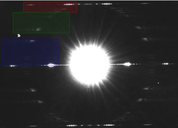
Fig. 2.1.3 Simulated electron diffraction pattern of (18, 3) chiral carbon nanotube.
Uppercase letters are used for labeling the layer lines in the simulation. (simulation from
http://www.physics.unc.edu/project/lcqin/www1/nds/hdsh/hdsh.html).
2.2 Imaging of CNT by TEM
The analytical techniques to characterize carbon nanotubes include (but are not limited
to) transmission electron microscopy (TEM), Raman spectroscopy, and scanning probe
microscopy. The simultaneous imaging and diffraction capabilities that a TEM provides
have made it the primary instrument over the years to study such sub-nanometer
study of the structure, the diameter and the crystallinity of carbon nanotubes. However,
great caution must be taken when it comes to interpreting TEM images of carbon
nanotubes for the determination of the structure and the diameter since they are not free
of imperfections.
2.2.1 Theory
There are two major contrast mechanisms used in TEM to create an image of a
specimen: amplitude contrast and phase contrast. The amplitude contrast is obtained in an
image if a small objective aperture is used to exclude most scattered electron beams
except the selected beam. The areas of the specimen with higher mass or stronger atomic
potential will scatter more electrons toward larger angular regions (regions away from the
optical axis and the central beam) and will appear dark in the images. Phase contrast
results from the differences in the phases of the electron waves scattered through a thin
specimen. In a phase contrast image, a larger objective aperture is usually used to allow
more scattered beams to pass through the objective lens to form a final image. It offers
higher resolution on the structure imaged and it is usually called HRTEM. The HRTEM
images of carbon nanotubes in the literature mostly refer to phase contrast imaging
conditions. It is very sensitive to the imaging conditions such as specimen thickness,
orientation, scattering factor of the specimen, aberrations and variations in defocus value
of the objective lens. These all make phase contrast images difficult to interpret but this
high level of sensitivity is what makes the imaging of atomic structure in a specimen
32
An electron microscope transforms each point in the specimen into a disk in the final
image. If we represent the specimen by a specimen function t(x,y) then a point (x,y) in
the specimen is transformed to a region defined by g(x,y) in the image. This can be
written mathematically as [11]
g(rr)=t(rr)⊗h(rr). (2.2.1)
) (r
g r is called the convolution of t(rr) with h(rr) where h(rr) is called the point spread
function of the microscope since it spreads a point into a disk. We see disks in the image
because the imaging system is not perfect. Moreover, more than one point in the
specimen might contribute to what we see in the final image since the disks could
overlap. Therefore, what we need to do is to correlate what we see in the image with the
structure of the specimen in a linear fashion [11].
The high resolution seen in an image means high spatial frequencies required to form
an image. This means the beams diffracted far away from the optical axis should be
included in the image-forming field of the objective lens to increase the fine details
observed in a final image. The beams away from the optical axis will be bent at greater
angles by the objective lens and these beams will be focused at a point different than
those beams closer to the optical axis because of spherical aberration of the lens. This
will cause a loss of fine detail in the final image. Thus, the resolution of an electron
microscope is limited by the spherical aberration of the objective lens.
To be able to simulate or interpret phase contrast images of a thin specimen, first we
need to formulate the specimen structure. In an electron microscope column, we can
consider the electrons moving along the optical axis (z-direction) incident on the
Ψ(zr)=exp(2
π
iuzz)=exp(2π
iz/λ
), (2.2.2)where λ is the wavelength of the electron and uz is the propagation wave vector along the
z-axis. The relativistic expression for the electron wavelength in vacuum is
) 2
( m0c2 eV eV
hc
+ =
λ
. (2.2.3)In the expression, m0 is the rest mass of the electron and V is the accelerating voltage of
the microscope (eV is the kinetic energy of the electron). For modern microscopes, the
energy of the incident electrons is much higher than that of the electrons in the specimen.
For a thin specimen, the electrons interact with the weak electrostatic potential of the
specimen when they are transmitted through it and acquire a phase factor at the exit face.
The wave function transmitted through the specimen at the exit face is the multiplication
of the incident plane wave by the specimen transmission function:
t t(r) (z) t(r)exp(2πiz/λ) r r r = Ψ =
Ψ (2.2.4)
and
t(rr)=exp[i
σ
Vz(rr)]. (2.2.5)In the transmission function, σ is the interaction constant (not scattering cross-section)
and Vz(rr) is the projected atomic potential of the specimen along the z-axis. Vz(rr) is the
integral of the 3D specimen potential along the optical axis:
Vz(rr)=Vz(x,y)=
∫
Vs(x,y,z)dz. (2.2.6)The interaction constant is σ =2πmeλ/h2 where m is the relativistic mass of the electron
34
specimen is thin so that the potential inside is small and the specimen structure can be
projected on two dimensions by a simple integral along z-axis. In the weak phase object
approximation (WPOA), Vz(x, y) is much smaller than one so that the exponential term
in the transmission function can be expanded as (neglecting higher order terms in
expansion)
t(r)=1+iσVz(x,y) r
. (2.2.7)
The WPOA is telling us that the amplitude of the transmission function is linearly related
to the projected structure of specimen [11].
At the back focal plane of the objective lens, the transmission function of the
specimen will be received and propagated through to contribute to the final image
contrast by the transfer function of the lens. Equation (2.2.1) can be rewritten in terms of
Fourier transforms in the reciprocal space:
G(ur)=T(ur)H(ur) (2.2.8)
and
H(ur)= A(ur)E(ur)exp[iχ(ur)]. (2.2.9)
A convolution of two functions in real space is the multiplication of their Fourier
transforms in reciprocal space. Here T(ur) is Fourier transform of the transmission
function of the specimen which arrives at the back focal plane (we ignored the phase term
due to plane waves because we are looking for the intensity in the final image). The
transmitted electrons at the back focal plane are collected by the objective lens and
modified by its contrast transform function H(ur) to form the final image in the imaging
plane. In H(ur), A(ur) is the aperture function, E(ur) is the envelope function and χ(ur)
value ∆f of the objective lens, which is also known as the aberration function or
phase-distortion function [11] :
χ(u)=π∆fλu2 +0.5πCsλ3u4
r
. (2.2.10)
The image wave function will be an inverse Fourier transform of equation (2.2.8) in the
image plane:
i FT 1[G(u)] r
−
=
Ψ . (2.2.11)
Then the image intensity g(x,y) will be the square modulus of the wave function in real
space in the image plane of the objective lens:
g(r) i2 t(r) h(r)2 r r r ⊗ = Ψ
= . (2.2.12)
In the WPOA theory, we know that only the imaginary part of H(ur) will contribute to
the contrast in the final image [11, 12]. Thus we can rewrite the contrast transfer function
in terms of the sine of the phase-distortion function:
B(ur)= A(ur)E(ur)sin[χ(ur)]. (2.2.13)
Even though B(ur) is not identical to H(ur), sometimes B(ur) is called the contrast
transfer function. In the aperture term, the objective lens aperture will collect only the
diffracted beams falling inside and cut off all others larger than the value defined by the
radius of the aperture [11, 12].
If we ignore the envelope function and take the aperture function as unity for the
beams falling inside the objective aperture and zero for all other beams, then sin[χ(ur)]
will be solely responsible for the output of the transmission system and the image
36 50
− =
∆f nm for a TEM (like JEOL JEM-2010F for example). In the calculated
functions we see the band of constant transmission and an oscillatory band with zeros. In
an ideal contrast transfer function one would like to see a constant horizontal line. The
oscillatory behavior means that the CTF acts like a band-pass filter and the high
frequency part of the spectrum is filtered out and makes no contribution in the final
image. The optimum CTF is the one that has the fewest zeros and an almost constant
spectrum in transmission. The effect of spherical aberration of the objective lens and the
negative defocus value can be balanced against each other and such imaging condition is
known as the “Scherzer defocus” [11,12]. At the Scherzer defocus, all diffracted beams
have almost a constant phase until the first cross-over of the horizontal axis which defines
the optical resolution of the imaging system. This is also known as the Scherzer
resolution and it is the best that we can expect from the microscope [11, 12]. This is not
the information limit but it’s the limit to what we can interpret intuitively from the
images:
∆fsch=−1.2(Csλ)1/2 (2.2.14)
and
rsch=0.66Cs1/4λ3/4. (2.2.15)
The ultimate resolution or the information limit of the microscope will be determined by
other factors like energy spread, chromatic aberration and electrical instabilities that are
included in the envelope function. The final form of contrast transfer function will be
obtained by multiplying the phase-distortion function with the envelope function. The
effect of the envelope function will be a sharp cut-off of the spectrum at high spatial
information limit and any information beyond this limit can only be retrieved by
sophisticated image analysis processes. The Scherzer resolution will still be the directly
interpretable limit read from the images.
Fig. 2.2.1 The contrast transfer function calculated for JEOL JEM-2010F at the defocus
values of (a) -30 nm and (b) -50 nm, respectively. The red arrows indicate the first
38
2.2.2 TEM Images of CNT
The images of carbon nanotubes can be interpreted in terms of the WPOA theory. A
SWNT has only two atomic layers of carbon at the top and the bottom in the electron
beam direction. The top and bottom atomic layers are parallel to one another and
perpendicular to the electron beam except near the edges of the tube. Moreover, the
carbon atoms are weak scatterers for energetic electrons due to the low atomic number
(Z=6) of carbon. A high-resolution image of a SWNT can be easily obtained using a
modern TEM equipped with a field emission gun. Ignoring image deteriorations due to
thermal and mechanical vibrations and the stage drift, the final image will give the
ultimate structure of the SWNT in terms of the projected potential of the tube. However,
no electron microscope is perfect. The projected potential of the tube will be deteriorated
because of vibrations, aberrations and electrical instabilities of the lenses.
Figure 2.2.2 shows high resolution TEM images of a SWNT, a double-walled
(DWNT) and a few-walled carbon nanotube (FWNT) together with their cross sections.
We see two hollow concentric cylinders in a cross section of the DWNT for example.
What we see in its HRTEM image is two parallel dark lines that run along the tubule axis.
The dark lines are the projected structure of the tube at the edges. The diameter of the
inner and outer shells can be measured using the dark lines in the images. We need to be
cautious of the fact that the structure seen in the images is very sensitive to the imaging
conditions. The widths of the dark lines seen in images vary with the defocus of the
objective lens and the contrast might not be uniform inside the dark lines [13]. This
makes the determination of the diameter more obscure because the diameter values will
Fig. 2.2.2 Electron micrographs of a SWNT (a), a DWNT (b) and a FWNT (c) with four
walls. The cross-sections of each nanotube are shown at bottom. The scale bar is same for
40
The error in diameter measurements becomes more significant for the smaller tubes
due to the pronounced curvature [13]. There are other important factors that need to be
taken into account when the carbon nanotubes are imaged inside the TEM for structural
measurements. The orientation of the nanotube with respect to the electron beam is one
of them. In most imaging situations, it is assumed that the nanotube lies on a flat plane
perpendicular to the incident beam direction. The tilt of the plane of the nanotube or the
rotation of the nanotube about the tube axis is additional sources of error in diameter
measurements [13, 14]. The other situation that needs to be avoided is imaging of
nanotubes when they overlap with thin amorphous carbon films [15].
The smallest of the carbon nanotubes were discovered with HRTEM. The first
discovery was the synthesis of a 0.4 nm diameter carbon nanotube inside a multi-walled
carbon nanotube [16]. Later this was followed by the news of the smallest nanotube yet
with a 0.3 nm diameter, inside a MWNT [17]. The formation of an individual SWNT as
small as 0.3 nm in diameter was also observed using high resolution TEM [18]. When we
use TEM to study such sub-nanometer scale materials, caution must be taken.
Sometimes, a ghost image appears in TEM micrographs due to the coherently scattered
electrons with the use of field emission gun and improper focusing conditions [14]. This
also makes the imaging and interpretation of bundles of nanotubes difficult to figure out
if they are composed out of the SWNTs or DWNTs only. Fig. 2.2.3 illustrates the
observation of a small carbon nanotube inside a MWNT due to use of a field emission
gun and improper defocus. The MWNT seems to be completely filled inside with the
innermost tube being 0.4 nm in diameter. A focus series of images of the same tube needs
Fig. 2.2.3 Electron microscopy images of a MWNT taken at two different defocus values.
The scale bar is same for both images. The image on the right shows the appearance of a
42
2.3 References
1. Cochran, W., Crick, F. H. C., Vand, V. (1952). The structure of synthetic polypeptides. I. The transform of atoms on a helix. Acta Cryst. 5, 581-586.
2. Qin, L. C. (1994). Electron diffraction from cylindrical nanotubes. J. Mater. Res. 9, 2450-2456.
3. Lucas, A. A., Bruyninckx, V., Lambin, Ph. (1996). Calculating the diffraction of electrons or X-rays by carbon nanotubes. Europhysics Lett. 35, 355-360.
4. Lambin, Ph., Lucas, A. A. (1997). Quantitative theory of diffraction by carbon nanotubes. Phys. Rev. B56, 3571-3574.
5. Liu, Z., Zhang, Q., Qin, L. C. (2000). Determination and mapping of diameter and helicity for single-walled carbon nanotubes using nano-beam electron diffraction. Phys. Rev. B71, 245413.
6. Qin, L. C. (2006). Electron diffraction from carbon nanotubes. Rep. Prog. Phys.
69, 2761-2821.
7. Liu, Z., and Qin, L.C. (2004). Symmetry of electron diffraction from single-walled carbon nanotubes. Chem. Phys. Lett.400, 430-435.
8. Qin, L. C. (2007). Determination of the chiral indices of carbon nanotubes by electron diffraction. Phys. Chem. Chem. Phys. 9, 31-48.
9. Gao, M., Zuo, J. M., Twesten, R. D., Petrov, I., Nagahara, L. A., Zhang, R. (2003). Structure determination of individual single-walled carbon nanotubes by nano-area electron diffraction. Appl. Phys. Lett. 82, 2703-2705.
10. Liu, Z., Zhang, Q., Qin, L.C. (2005). Accurate determination of atomic structure of multiwalled carbon nanotubes by nondestructive nanobeam electron diffraction. Appl. Phys. Lett. 86, 191003.
11. Williams, D. B. and Carter, C. B. (1996). Transmission electron microscopy. New York: Plenum Press.
13. Qin, Q. and Peng, L. M. (2002). Measurement accuracy of the diameter of a carbon nanotube from TEM images. Phys. Rev. B65, 155431.
14. Hayashi, T., Muramatsu, H., Kim, Y. A., Kajitani, H., Imai, S., Kawakami, H., Kobayashi, M., Matoba, T., Endo, M., Dresselhaus, M. S. (2006). TEM image simulation study of small carbon nanotubes and carbon nanowires. Carbon 44, 1130-1136.
15. Qin, L. C., Zhao, X., Hirahara, K., Ando, Y., Iijima, S. (2001). Electron microscopic imaging and contrast of smallest carbon nanotubes. Chem. Phys. Lett. 349, 389-393.
16. Qin, L. C., Zhao, X., Hirahara, K., Miyamoto, Y., Ando, Y., Iijima, S. (2000). The smallest carbon nanotube. Nature408, 50.
17. Zhao, X., Liu, Y., Inoue, S., Suzuki, T., Jones, R. O., Ando, Y. (2004). Smallest carbon nanotube is 3 Ǻ in diameter. Phys. Rev. Lett. 92, 125502.
18. Peng, L. M., Zhang, Z. L., Xue, Z. Q., Wu, Q. D., Gu, Z. N., Pettifor, D. G. (2000). Stability of carbon nanotubes: How small can they be? Phys. Rev. Lett.