HBM Tester Waveforms, Equivalent Circuits, and Socket
Capacitance
Timothy J. Maloney
Intel Corporation, 2200 Mission College Blvd., SC9-09, Santa Clara, CA 95054 USA tel.: 408-765-9389 e-mail: [email protected]
This paper is co-copyrighted by Intel Corporation and the ESD Association
Abstract - The Tektronix CT2 current probe is used to acquire more accurate Human Body Model waveforms with 0-ohm and 500 ohm tester loads than a CT1, owing to the CT2’s low-frequency performance. The integrals and centroids of these waveforms then readily yield precise values of tester circuit elements and effective socket capacitance. Expressions are derived for effective socket capacitance resulting from distributed capacitance along a transmission line connecting to an unmatched load. These lead to options for reducing the effective socket capacitance while retaining the lines for delivering the HBM pulse.
I. Introduction
It was shown in 2009 [1] that HBM waveforms taken with a 0-ohm standard test load using a current probe can yield basic circuit modeling values for the tester,
such as the charging capacitance Chb, the time
constant RhbChb, and thus the series resistance Rhb.
These parameters are extracted from “moments” of the waveform (integral and centroid, or 0th and 1st
moments in this case) as described in [1], and extend from circuit analysis dating back to the Elmore theorem [2]. While obtaining Chb from integrated
current was fairly obvious, it was the Elmore theorem applied to the 2-pole RLC model of HBM that showed the ease of extracting true RhbChb, irrespective of
inductance L1. While Ref. 1 cautioned that current
measurements extracted with a CT1 current probe may have to be corrected for low frequency response of the probe, it is now found that the CT2 probe (also from Tektronix, Inc.) can provide good data for HBM tester characterization and circuit modeling, without significant need for correction.
The analytical methods of [1] can now be extended to a 4-pole model as used heavily for HBM work in the 1990s [3,4], to obtain circuit modeling information quickly and simply. As in [3], standard waveform measurements with loads of 0 and 500 ohms are used to deduce values of the parameters, notably Chb, Rhb
and socket capacitance C2. Chb and Rhb are the basic
human body model parameters, of course, while socket capacitance needs to be limited because it
produces extra stress on many ESD protection devices, stress that could be inappropriately destructive. This was well recognized in the 1990s and [3] presented electrothermal simulations showing the extent of that extra stress. Also, if a no-connect (NC) pin is stressed, the air will break down starting at about 800V and discharge the entire socket capacitance immediately, usually to a neighboring pin, producing an event far more destructive than HBM at the same voltage [5]. Ref. 3 also showed how difficult it was to achieve “selectivity” against high values of C2 using only rise time and peak
current standards with 0 and 500 ohms. To determine C2 accurately seemed to require computer-driven
multi-parameter analysis and curve fitting. In this work, we find that C2 is far more accessible than we
thought, through analysis of waveform moments. Highly “selective” methods for finding equivalent C2
could be adopted if we wish, or at least we could quickly determine the C2 of a tester that might
produce a problem with a device during HBM testing.
II. Analytical Foundations
1. Extraction of s-domain Functions
∫
∞−
=
0dt
e
t
h
s
H
(
)
(
)
st∫
∞⋅⋅
⋅
+
−
+
−
=
0
3 3 2 2
6
2
1
st
s
t
s
t
dt
t
h
(
)[
]
∑
∞∫
=
∞
−
=
0 0
1
kk k k
dt
t
h
t
s
k
!
(
)
.
)
(
(1)
The various terms in the series are moments of the waveform, which yield coefficients of a Laplace domain function H(s) = a0+a1s+a2s2+… While an
acceptable way of determining those coefficients, given a digital oscilloscope waveform h(t), would be to do the time integrals as in (1) (and discussed in [1] in terms of integration by parts), the Laplace transform formulation itself offers a more efficient and more easily implemented algorithm that was briefly treated in [1].
In this work, h(t) will be some kind of HBM
waveform. Equation (1) tells us that the a0 coefficient
of H(s) is simply the integral h(t) from start to finish. But the Laplace treatment also tells us that this
integral function =
∫
t
d h t h
0
1( ) (
τ
)τ
transforms toH1(s) = H(s)/s = a0/s+a1+a2s+…, as 1/s is the
integration operator in the Laplace domain. Essentially, h1(t) is a step of height a0 with other
features given by the rest of the coefficients. The Elmore Delay is indicated by a1, after normalizing to
a0 and accounting for the (-1) factor. The next
time-dependent function of interest thus subtracts the basic
step height a0 from h1(t), i.e.,
∫
−= t h d a t
h
0
0 '
1( ) (
τ
)τ
for which the transform isH1’(s) = a1+a2s+a3s2+… We are back where we
started with H(s), and know to find a1 by integrating
h1’(t) to get h2(t), then noting the step height again.
The integral this time is the “area capture” integral as shown in [1], Fig. 9, and also later in this work, Fig. 6. Because we subtracted the step height to form h1’(t),
the integral is, strictly speaking, negative in our example, but that is expected from the (-1) factor for that term in Eq. 1, given a positive waveform. Thus the Elmore Delay (-a1/a0) is positive, as expected.
With digital data and integration with (for example) a spreadsheet program, we can determine any and all coefficients through iteration as above. For many waveforms therefore, particularly a smooth one like HBM, the s-domain function H(s) is thus available,
rather easily, to a number of coefficients (limited only by noise) and can be related to circuit models that predict those coefficients.
The above algorithm is very time-efficient on the computer if one is interested in a low-order polynomial, i.e., just the first few s-coefficients for acquiring circuit element knowledge. For N digital points in the scope waveform, the integral for each coefficient is of order N in time complexity, so for q coefficients, there are on the order of Nq operations (O(Nq)). In this work, we will find that q=2 applied to each waveform will be enough to determine our circuit elements. In contrast, using a fast Fourier transform (FFT) algorithm would have O(N*log2N)
time complexity and would give N/2 frequency components, but this is far more information than needed for circuit modeling. The zero-frequency FFT component would correspond to a0 but we would still
have to take a derivative near zero frequency to find a1. Even so, given that modern digital oscilloscopes
usually offer quick FFT conversion of a waveform to the frequency domain, one may well want to use that
FFT function to extract a0 and a1 (or more
coefficients) quickly with a user-defined math function on the scope.
2. Transformers and Their Transfer Functions
Another aspect of the 2009 work [1] that we will use is the notion of a transfer function for transformers, such as the CT1 and CT2 current transformers for HBM that this paper discusses. As shown in [1], the low frequency cutoff of the transformer is an important property because it describes the “droop” experienced as the transformer tries to follow the HBM waveform out into the decay time of 150 ns and beyond. To a remarkable degree, for a given current level the step response of one of these transformers is an exponential decay, as in Figure 1, so a single pole can describe the transfer function for that aspect. Another pole can describe high frequency rolloff, in which case the complete transfer function for a current transformer like the CT1 or CT2 can be approximated, ignoring normalization factors, by
)
)(
(
)
(
b
s
a
s
s
s
T
+
+
=
(2),where a=1/τxf, as in Fig. 1 and Ref. 1, and b=1/τhf,
focus on the a frequency or τxf. τxf is
current-dependent for both CT1 and CT2 probes, but while it is around 6.35 µsec for the CT1, it can be well over 100 µsec for the CT2. That will be significant.
Figure 1. Step response of a transformer; τxf is the 1/e decay time.
With two poles, the step response of the transformer is a double exponential, with a fast rise time. The impulse response of the transformer is, as usual, the derivative of the step response, and it is the impulse response that gives us, through convolution [8], the observed HBM waveform. The near-delta function in the current probe’s impulse response near t=0 will faithfully reproduce the HBM waveform, but it is the negative slope of the step response that gives us a weak or strong negative multiplier for the real HBM waveform in convolution. That is why a long τxf is
desired for fidelity.
III. HBM Waveform Measurement
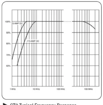
The Tektronix CT1 current probe [9] has traditionally been used for HBM waveform characterization [3]. Its high-frequency cutoff, approaching 1 GHz, is excellent for HBM rise times and peak currents, but its low-frequency cutoff is upwards of 100 kHz (Figure 2a) and causes noticeable sag in step response even at the 1 microsecond level [1]. Impulse response therefore has a strong negative component (imagine differentiating Fig. 1), and convolving such a response with the actual current waveform means that the decaying HBM current tail is depressed, and eventually drops below zero noticeably. This has surely caused systematic error in most measurements of HBM decay constant. Data taken with a CT1 can be corrected [1], but distortions are current-dependent [9], so it can be difficult to correct data accurately. The Tektronix CT2 probe [9] has been found to be more suitable for HBM waveform measurement.
Low-frequency cutoff is in the 1-10 kHz range (Figure 2b), which much better fits the HBM decay time of 150 nsec. Corrections are therefore negligible, and within electrical noise limits. This is indicated in Figure 3, comparing a section of the decay tail for the CT1 and CT2 probes on the very same pulse. The plunge below zero is clearly seen for the CT1. Meanwhile, rise time curves and peak current for 0 and 500 ohm loads are almost indistinguishable for CT2 versus CT1. In this case of a Thermo MK-4 tester, there was less than 1 per cent difference for those features, with 6-7 ns rise time for a 0 ohm load. The CT1 probe can always be used for rise time or peak current if there are any doubts about the CT2, but manufacturer data [9] indicates the impact of the CT2 bandwidth on those parameters may be negligible. At the same time, numerous measurements of the decay constant with the CT1 have shown that its droop, caused by low frequency response, is responsible for 0-ohm load decay constants failing the 130 ns minimum spec [11], particularly at 4kV, where distortion is greater. The CT2 then shows this “failure” to be a CT1 measurement artifact and not a tester fault. Use of the CT2 as the primary current probe for HBM waveforms is thus recommended.
Figure 2a. Tektronix CT1 probe data, from [9].
IV.
4-pole HBM Model and Circuit
Parameter Extraction
The traditional four-pole model (also called 4th order
model) of HBM is shown in Figure 4, with elements
V
t
labeled as in [3]. One slight but important difference is the added voltage source, pictured as a step because we are indeed taking the circuit from charged Chb to
zero volts. We therefore are interested in the total admittance and response to a voltage step, giving the current.
Figure 2b. Tektronix CT2 probe data, from [9].
CT2 and CT1, 500 ohm
-0.01 -0.005 0 0.005 0.01 0.015 0.02 0.025 0.03
760 780 800 820 840 860 880 900 920
time, nsec
cu
rre
n
t,
A
Figure 3. Expanded view of 500 ohm HBM tails for CT1 (lower) and CT2 (upper) current probes, with CT1 signal going negative because of its low frequency cutoff.
Approximate values of the circuit elements are as follows:
Rhb =1500 ohms
Chb =100 pF
C1 ≈ 2 pF
L1 ≈ 10 µH
R1 = 0 or 500 ohms
C2 ≈ 20 to 50 pF
Figure 4. 4th order model of HBM ESD tester, including parasitic capacitances and inductance. As Chb is initially charged to + or
-V0 and then discharges, HBM is conceptually the step response
of this network.
It has long been recognized [3,4] that C2 is the result
of distributed capacitance, and therefore will depend
on how R1 compares to the effective Z of the
transmission line. Ref. 3 found that 500 ohms was high enough to reveal nearly all of C2. We discuss
more about distributed capacitance in the next section. The admittance functions for the circuit in Figure 4 can be written with standard methods in the Laplace domain, and reduced to expressions for the currents we can measure with a current probe in series with R1,
resembling some of the work done in [1]. The full admittance function in the s-domain for the 4-pole network is
(3)
The step voltage is V=V0/s. For 0 ohms, C2 drops out,
the network is 3rd order, and we measure the full
current as
,
1
)
1
(
)
(
30 3 2 0 2 0 1
1 0
0
s
b
s
b
s
b
s
C
R
C
V
s
I
hb hb− −
−
+
+
+
+
=
(4) whereb1-0=Rhb(Chb+C1), b2-0=L1Chb, b3-0=L1ChbRhbC1.
Full current is hard to measure for nonzero R1, and is
treated in Appendix A. For R1=500 ohms, the current
in the 500 ohm branch is
, 1
) 1
( )
( 4
500 4 3 500 3 2 500 2 500 1
1 0
500
s b s b s b s b
s C R C
V s
I hb hb
− −
−
− + + +
+
+ =
(5) where b1-500=Rhb(Chb+C1)+R1(Chb+C2),
b2-500=RhbR1(Chb(C2+C1)+C2C1)+L1Chb,
b3-500=L1Chb(RhbC1+R1C2), and
CT1 CT2
C1
Chb
Rhb
L1
C2 R1
V0
1
1
1
1 21
1 2
1
+
+
+
+
+
=
s
s
C
R
C
R
s
s
C
R
C
R
s
C
L
s
C
s
Y
hb
hb hb hb hb
hb
)
b4-500=L1Chb(RhbC1R1C2). In both cases the 0th order
response is the total charge, Qt=V0Chb. Figure 5
shows 0 and 500 ohm test load waveforms for a Thermo MK-4 tester with a CT2 probe, both revealing a capacitance Chb of about 114 pF.
Figure 5. 0 and 500 ohm test load waveforms, 1kV, CT2 probe, measuring Qt=114 nC in each case for an MK-4 tester.
Things get interesting as we investigate centroids of these waveforms, following the methods in [1] and as described in Section II above. In particular, [1] and Section II proved that the area A above the integrated current curve, divided by Qt, gives the centroid of the
original waveform (units of time), as shown in Figure 6. The centroids τ0 and τ500 are of course the
first-order s-coefficients (times -1) of the series expansions of the current expressions (4) and (5), again following [1]:
).
(
)
(
)
(
.
)
(
2 1
1 2
1 1
1 500
1 500
1 1
1 0
1 0
C
C
R
C
R
C
R
C
C
R
C
C
R
C
R
b
C
R
C
R
C
C
R
C
R
b
hb hb
hb
hb hb
hb hb
hb
hb hb hb
hb hb hb
+
+
=
−
+
+
+
=
−
=
=
−
+
=
−
=
− −
τ
τ
(6)
Note that τ0 is unchanged from the simple 2-pole
model in [1]. In (5), let R1 be the true value of the
500 ohm resistor, R500. The socket capacitance C2
therefore is
hb
C R
C = − −
500 0 500 2
τ
τ
(7)
Note that C1 and L1 have dropped out of the analysis
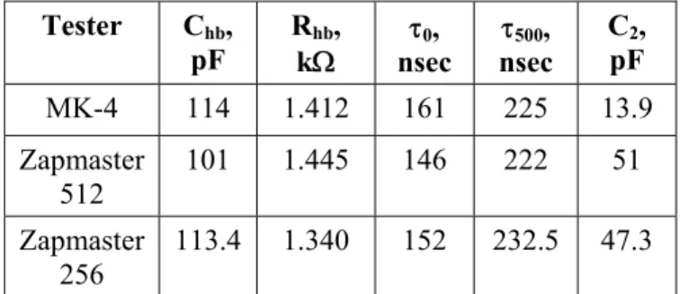
and appear only in higher order moments. For the MK-4 tester discussed above, the complete set of extracted values is listed in Table I. The socket capacitance C2=13.9 pF is considered a very good
result, and indeed the waveforms easily passed all specs related to socket capacitance.
Tester Chb,
pF
Rhb,
kΩ nsec τ0,
τ500,
nsec
C2,
pF
MK-4 114 1.412 161 225 13.9 Zapmaster
512
101 1.445 146 222 51
Zapmaster 256
113.4 1.340 152 232.5 47.3
Table I. Major circuit model values and time constants for three different HBM testers at two different sites, using CT2 probe and 0 and 500 ohm (R500=500-501 ohm) loads.
At the same time, older Zapmaster HBM testers, configured for 512 and 256 pins, at two different Intel sites, gave Rhb and Chb values as shown (see Table I),
but with higher socket capacitance C2=47-51 pF. Sure
enough, in the 512 case the 500 ohm Ipeak value did not pass spec. The 0-ohm load decay for the 512 was short enough that it failed on a CT1 probe (128 ns) but passed on a CT2 (135 ns). The 256 waveforms narrowly passed specs on the CT1 but had much healthier margins on the CT2. All this is in agreement with the notion that JEDEC and ESDA HBM specs were formulated with the intention of tolerating up to 50 pF of equivalent socket capacitance.
Figure 6. Integrated current for a 1 kV HBM waveform, converging to total charge Qt. The centroid τ of the original
waveform is computed from A/Qt = τ, where A is the area above
the curve, and is the Elmore Delay of this integrated current curve. Related theorems are proven in [1].
V. Distributed Socket Capacitance
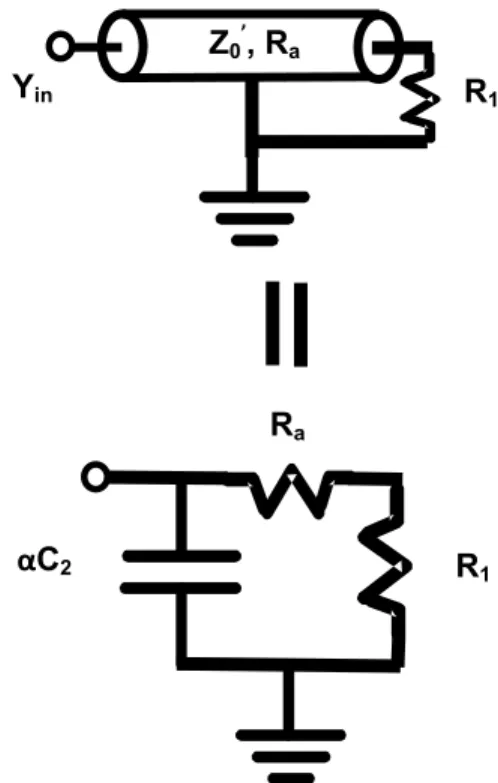
An automated HBM ESD tester acquires much of its apparent inductance L1 and socket capacitance C2from the distributed transmission lines through the relays to the socket board. That portion of the lumped element model as in Fig. 4 can be found from a first order approximation of the transmission line model, terminated by resistance R1 (0 and 500 ohms) with
line impedance Z0=1/Y0. This is illustrated in Figure
τ
= 166 ns
7, for which we want to find a simple network equivalent of Zin or Yin. For R1=0, there will be some
L1 and no C2, but from Eqs. 1-7, it is clear that L1 does
not affect the first-order C2 calculation that we arrive
at in Eq. 7 once we have a lumped model. Thus we turn to the case of R1=500 ohms and look at the input
admittance, aiming for in
j
C
xY
sC
xR
Y
=
+
=
1+
1
1
ω
Figure 7. HBM circuit model with distributed inductance and capacitance (L1 and C2 as in Fig. 4) shown as a transmission line
from the HBM network module to the socket load R1. Zin (equal
to 1/Yin) is expected to yield equivalent C2.
and effective capacitance Cx. From transmission line
theory [10],
l
l
l
l
LC
Y
Y
s
LC
sY
Y
Y
Y
Y
Y
Y
Y
in1 0 0 1
1 0
0 1 0
1
tanh
tanh
+
+
≈
⎥
⎦
⎤
⎢
⎣
⎡
+
+
=
γ
γ
, (8)
for low values of γℓ, γ the propagation constant
jω√LC=s√LC, L and C the capacitance and
inductance of the line per unit length, and ℓ the line length. Also Y02=C/L for the lossless transmission
line. To first order, the denominator expands for low values of γℓ to multiply the numerator, resulting in
L
+
−
+
=
LC
l
Y
Y
Y
s
Y
Y
in0 2 1 2 0
1 (9)
If the full distributed capacitance is C2=Cℓ, this
becomes
.
1
)
1
(
1
2 1
2 1
2 0 2 1
C
s
R
R
Z
sC
R
Y
in≈
+
−
=
+
α
(10)As expected, the effective capacitance Cx=αC2
declines with higher Z0 and tunes out completely with
an impedance match of R1=Z0. This means that one
strategy for reducing Cx is to raise the effective Z0,
say by distributing nearly lossless “loading coils” (e.g., ferrite beads) along the line. This recalls a coil loading method used in the 19th century to reduce the
resistive attenuation of telegraph signals, as the attenuation length is approximately 2Z0/R, R the
resistance per unit length [10], although the purpose here is slightly different. The extra total inductance puts some limits on the shortest achievable HBM rise time (see Appendix A), but the 2-10 ns window for 0-ohm loads [11], for example, should not be threatened by a few extra microhenries.
Figure 8. Expressions for the Yin of the distributed section of the
HBM model with total distributed resistance Ra give an equivalent
socket capacitance αC2 and parallel resistance as shown. Eq. (16)
is the general expression for the socket capacitance reduction factor α. The HBM network module resistance Rhb should be
reduced by (approximately) Ra in order to preserve the waveform
properties as discussed in Section IV.
Another way to reduce Cx is to borrow from the HBM
network’s 1500 ohms of series resistance and distribute some resistance Ra along the transmission
lines that also have their distributed capacitance
totaling C2. If the inductance now becomes
negligible,
γ
l
=
R
aC
2s
,2 0
sC R
Z = a , and
⎥ ⎥ ⎥ ⎥
⎦ ⎤
⎢ ⎢ ⎢ ⎢
⎣ ⎡
+ + =
l l
γ
γ
tanh tanh 1
1 0
1 0
0
R Z
R Z
Z
Zin
C1
Chb
Rhb
Z0
R1
V0
Zin
αC2
Z0’, Ra
Yin R1
R1
⎥ ⎥ ⎥ ⎥ ⎦ ⎤ ⎢ ⎢ ⎢ ⎢ ⎣ ⎡ + + = l l l l
γ
γ
γ
γ
2 1 0 1 0 0 tanh tanh tanh 1 tanh R Z R ZZ . (11)
But for small γℓ, tanhγℓ≈γℓ, Z0γℓ=Ra, and
2 1 1 2 1 1 1 1 1 sC R R R C sR R R R R R Z a a a a a in + + = ⎥ ⎥ ⎥ ⎥ ⎦ ⎤ ⎢ ⎢ ⎢ ⎢ ⎣ ⎡ + +
≈ . (12)
This means that
2 1
1
C
s
R
R
Y
ain
≈
+
+
α
, (13)where α=R1/(Ra+R1), and corresponds to the circuit
model in Figure 8. The effective capacitance Cx= αC2
and is reduced accordingly by the distributed resistance Ra. But if the total inductance Lt is not
negligible, Ra is simply replaced by Ra+sLt (=Z0γℓ) in
(12-13), leading us to a more general expression
⎥
⎥
⎥
⎥
⎦
⎤
⎢
⎢
⎢
⎢
⎣
⎡
⎟⎟
⎟
⎟
⎟
⎠
⎞
⎜⎜
⎜
⎜
⎜
⎝
⎛
+
′
+
+
⎥
⎦
⎤
⎢
⎣
⎡
+
=
1 2 2 0 1 1 2 11
1
1
R
R
s
C
Z
R
R
R
sC
R
Y
a ain . (14)
We now take
2
0 C
L
Z′ = t for the transmission line,
while the actual impedance is complex and includes the effect of Ra. Expanding this to first order, we have
⎥
⎦
⎤
⎢
⎣
⎡
⎟⎟
⎠
⎞
⎜⎜
⎝
⎛
+
′
−
+
+
+
≈
)
(
1
1
1 1 2 0 1 1 21
R
R
R
Z
R
R
R
sC
R
R
Y
a a a in . (15)This reduces to (10) for Ra=0 and to (13) for Lt or Z0'
negligible, so now we see that the general capacitance reduction factor is
⎟⎟ ⎠ ⎞ ⎜⎜ ⎝ ⎛ + ′ − + = ) ( 1 1 1 2 0 1 1 R R R Z R R R a a
α
(16)for a transmission line with inductive and resistive loading as above. From this expression, it can be easily shown that the tradeoff of Ra and Z0' is
particularly simple when α<0.5 is desired, as that condition is
2 1 2 0
2
2
Z
R
R
a+
′
>
. (17)Therefore when R1=500 ohms, α<0.5 is achieved with
300 ohms for each of Ra and Z0', for example, along
with other solutions beyond the elliptical boundary in the Ra- Z0' plane. Lower effective capacitance of this
kind also has the desired effect on sudden destructive currents that can be delivered in snapback [3] or in breakdown of a no-connect pulse [5], as the inductive and resistive loading limits the current.
VI. Conclusions
The Tektronix CT2 current probe is found to be adequate for short-time HBM waveform measurements like rise time and peak current, and more suitable than the same manufacturer’s CT1 probe for long-time measurements like decay constant. CT2 waveforms do not suffer from significant droop in HBM waveform tails, making them suitable for circuit element extraction through asymptotic waveform analysis methods, even with a 4-pole model of HBM.
Integration of the 0-ohm load waveform gives main
HBM capacitance Chb, and the waveform’s first
moment or centroid gives the RhbChb time constant τ0
and therefore Rhb, through straightforward and
essentially graphical means. While the authors of Ref. 3 found that only a careful multi-parameter fit to waveforms could determine a best value of C2, the
methods here, summarized by Eq. 7, allow tester equivalent socket capacitance C2 to be accurately
measured from the 0-ohm values (Chb, τ0) plus the 500
ohm centroid time constant. This allows a precise measurement of this important value with a simple, easily accessible method, as the error in C2 should be
limited only by noise and numerical accuracy. The method leading up to Eq. 7 provides the “selectivity” for C2 that has long been sought by ESD researchers.
A related qualification standard would depend on acceptance of digital waveform records and procedures for extracting simple integrals and centroids from the waveforms.
Much of the effective socket capacitance αC2 in an
HBM tester can result from the necessarily long distribution lines from the HBM network module to the component at the socket. The network analysis methods of this paper are extended to find the effective socket capacitance that results from (1) the known finite impedance and terminating load of the transmission line, and (2) distributing some of the required 1500 ohms of series resistance throughout this transmission line. Simple general expressions for
αC2 then show how inductive loading and/or
this capacitance and thus reduce unwanted extra stress during the HBM test. Newer HBM testers have much lower αC2 and are already using these methods.
Appendix A: Additional
Mathematics
For nonzero R1, the full current is found from Eq. 3 to
be . 1 ) 1 )( 1 ( ) ( 4 500 4 3 500 3 2 500 2 500 1 2 1 1 0 500 s b s b s b s b s C R s C R C V s
I hb hb
full − − − − − + + + + + + = (A1)
This is Eq. 5 with one more zero. Thus the measured I500(t) is the convolution of Ifull-500(t) with exp(-t/R1C2),
so for a fast rise time on Ifull-500(t), the R1C2 time
constant is expected to add to it and dominate the rise time of I500(t). HBM test standards [11] have agreed
with this.
Note that all these network functions are ratios of polynomials. The essential properties of the functions can be examined by considering each network function to be
,
1
1
)
(
2 2 1 2 2 1 m m n ns
b
s
b
s
b
s
a
s
a
s
a
s
H
+
⋅⋅
⋅
+
+
+
+
⋅⋅
⋅
+
+
+
=
(A2)m≥n, and corresponding to time domain function h(t). It is useful to expand H(s) about s=0 to obtain an infinite series in powers of s,
2 2 1 1 1 2 2 1
1
)
(
)
(
1
)
(
s
a
b
s
a
b
b
a
b
s
H
=
+
−
+
−
−
+
⋅⋅
⋅
+
−
+
−
+
−
−
+
3 31 2 1 1 1 2 2 1 2 1 3
3
2
)
(
a
b
a
b
b
b
a
b
a
b
b
s
(A3)
This kind of result appears in many works on signal integrity [6]. It is also useful to consider the factors of the numerator and denominator of H(s), described by the m poles pi and the n zeros zi that form the roots of
the polynomials. It is a consequence of Vieta’s Formulas describing the relations among symmetric polynomials Sq [12] of these roots to the coefficients
that we can form Sn-1/Sn for the poles and zeros and
find that
(A4)
Remember that the real parts of our poles and zeros will typically be negative numbers, and the coefficients positive real, so the minus signs can be dropped if we regard the reciprocal poles and zeros as positive time constants. Note also that complex conjugate poles or zeros σ±jω add together to become a real number 2σ/(σ2+ω2).
The fact that the poles and zeros sum to an easily calculated number can be used to refine some of our estimates. In the 1993 work by Verhaege, et al., [3], the main decay constant τ2 for the 4th order network is
found to be
τ2=(Rhb+R1)(Chb+C1). (A5)
For the shorting waveform R1=0, this reduces to
τ20=Rhb(Chb+C1). (A6)
However, in the expression for I0(s), Eq. 4, this
corresponds to b1-0, the sum of all the poles, including
rise time plus decay constant. It is clearly correct for L1=0, where everything collapses to a single pole, but
then the rise time would be zero and out of spec. Some influence of inductance is expected, as is the case for a 2-pole network (note that 1/a + 1/b = RhbChb). By starting with L1=R1=0 and adding in L1
as a “small” perturbation, one gets
(A7)
The last term indicates the rise time of the HBM network, with the expected L/R leading term.
Acknowledgements
The author would like to thank Russell Sears, Marti Farris and Abishai Daniel of Intel for the HBM tester data, acquired using both CT1 and CT2 current probes. Thanks also to Evan Grund for manuscript review and additional insights.
References
[1] Timothy J. Maloney, “Evaluating TLP Transients and HBM Waveforms”, EOS/ESD Symposium Proceedings, pp. 143-151, 2009.
[2] W.C. Elmore, “The Transient Analysis of Damped Linear Networks With Particular Regard to Wideband Amplifiers”, J. Appl. Phys. Vol. 19(1), pp. 55-63 (1948).
[3] K. Verhaege, P. Roussel, G. Groeseneken, H. Maes, H. Gieser, C. Russ, P. Egger, X. Guggenmos, and F. Kuper, “Analysis of HBM ESD Testers and Specifications Using a 4th Order Lumped Element Model”, EOS/ESD Symposium Proceedings, pp. 129-137, 1993.
[4] L. van Roozendaal, A. Amerasekera, P. Bos, W. Baelde, F. Bontekoe, P. Kersten, E. Korma, P. Rommers, P. Krys, U. Weber and P. Ashby, “Standard ESD Testing of Integrated Circuits”, . 1 , 1 1 1 1 1
∑
∑
= = − = − = n i i m i i a z b p)
)
(
2
1
(
)
(
2 1 2 1 1 1 1 20C
C
R
C
L
C
C
R
L
C
C
R
hb hb hb hb hb hbhb
+
−
−
+
+
EOS/ESD Symposium Proceedings, pp. 119-130, 1990.
[5] H. Kunz, C. Duvvury, J. Brodsky, P. Chakraborty, A. Jahanzeb, S. Marum, L. Ting, and J. Schichl, “HBM Stress of No-Connect IC Pins and Subsequent Arc-Over Events that Lead to Human-Metal-Discharge-Like Events into Unstressed Neighbor Pins”, EOS/ESD Symposium Proceedings, pp. 24-31, 2006.
[6] R. Gupta, B. Tutuianu, and L.T. Pileggi, “The Elmore Delay as a Bound for RC Trees with Generalized Input Signals”, IEEE Trans. on Computer-Aided Design of Integrated Circuits and Systems, vol 16, no. 1, pp. 95-104, January 1997.
[7] M. Celik, L. Pileggi, and A. Odabasioglu, IC Interconnect Analysis, (New York: Kluwer Academic Publishers, 2002).
[8] R.N. Bracewell, The Fourier Transform and Its Applications, (New York: McGraw-Hill, 1965).
[9] Web article, Tektronix page on CT1, CT2, and
CT6 current probes:
http://www2.tek.com/cmswpt/psdetails.lotr?ct=PS &lc=EN&ci=13500&cs=psu. Figs. 2a, 2b used with permission.
[10] S. Ramo, J. Whinnery, and T. Van Duzer, Fields and Waves in Communication Electronics, (New York: John Wiley & Sons, 1965), p. 46.
[11] ANSI/ESDA/JEDEC JS-001-2010, ESDA/JEDEC Joint Standard for Electrostatic Discharge Sensitivity Testing--Human Body Model (HBM)--Component Level (Jan. 2010). Available at www.jedec.org and www.esda.org. [12] Web articles,
http://mathworld.wolfram.com/PolynomialRoots. html, also
http://mathworld.wolfram.com/VietasFormulas.ht ml.
![Figure 2a. Tektronix CT1 probe data, from [9].](https://thumb-us.123doks.com/thumbv2/123dok_us/8195199.2172549/3.918.490.818.571.900/figure-a-tektronix-ct-probe-data-from.webp)