DEVELOPMENT AND CHARACTERIZATION OF AN IOT NETWORK FOR AGRICULTURAL IMAGING APPLICATIONS
A Thesis presented to
the Faculty of California Polytechnic State University, San Luis Obispo
In Partial Fulfillment of the Requirements for the Degree Master of Science in Electrical Engineering
by Jacob Wahl
COMMITTEE MEMBERSHIP
TITLE: Development and Characterization of an IoT Network for Agricultural Imaging Applications
AUTHOR: Jacob Wahl
DATE SUBMITTED: June 2020
COMMITTEE CHAIR: Jane Zhang, Ph.D.
Professor / Graduate Coordinator Department of Electrical Engineering
COMMITTEE MEMBER: Vladimir Prodanov, Ph.D. Associate Professor
Department of Electrical Engineering
COMMITTEE MEMBER: Bridget Benson, Ph.D. Associate Professor
ABSTRACT
Development and Characterization of an IoT Network for Agricultural Imaging Applications Jacob Wahl
Smart agriculture is an increasingly popular field in which the technology of wireless sensor networks (WSN) has played a large role. Significant research has been done at Cal Poly and elsewhere to develop a computer vision (CV) and machine learning (ML) pipeline to monitor crops and accurately predict crop yield numbers. By autonomously providing farmers with this data, both time and money are saved. During the past development of a prediction pipeline, the primary focuses were CV and ML processing while a lack of attention was given to the collection of quality image data. This lack of focus in previous research presented itself as incomplete and inefficient processing models. This thesis work attempts to solve this image acquisition problem through the initial development and design of an Internet of Things (IoT) prototype network to collect consistent image data with no human interaction. The system is developed with the goals of being low-power, low-cost, autonomous, and scalable. The proposed IoT network nodes are based on the ESP32 SoC and communicate over-the-air with the gateway node via Bluetooth Low Energy (BLE). In addition to BLE, the gateway node periodically uplinks image data via Wi-Fi to a cloud server to ensure the accessibility of collected data. This research develops all functionality of the network, comprehensively characterizes the power consumption of IoT nodes, and provides battery life estimates for sensor nodes. The sensor node developed consumes a peak current of 150mA in its active state and sleeps at 162µA in its standby state. Node-to-node BLE data transmission throughput of 220kbps and node-to-cloud Wi-Fi data transmission throughput of 709.5kbps is achieved. Sensor node device lifetime is estimated to be 682 days on a 6600mAh LiPo battery while acquiring five images per day. This network can be utilized by any application that requires a wireless sensor network (WSN), high data rates, low power consumption, short range communication, and large amounts of data to be transmitted at low frequency intervals.
ACKNOWLEDGMENTS
First and foremost, I would like to endlessly thank my parents and sisters for their constant love and for promoting the importance of education.
I would like to thank my advisor, Dr. Zhang, for offering support throughout this process and suggesting this topic to me. Thank you to Dr. Prodanov for recommending the development board used in this thesis and for valuable suggestions throughout my development process. Thank you to Dr. Benson for providing critical and constructive feedback of my paper.
I would like to thank my close friends Avery, Donald, Elysa, Faye, Jennie, Madi, and Sarah for the friendship and encouragement over the past five years. You all truly made Cal Poly a home and a wonderful place to learn, and I cannot thank you enough.
TABLE OF CONTENTS
Page
LIST OF TABLES ... x
LIST OF FIGURES ... xi
1. INTRODUCTION ... 1
1.1 Background and Overview ... 1
1.1.1 Technology in Agriculture ... 1
1.1.2 Motivation ... 1
1.1.3 Significance of Quality Data ... 3
1.2 Statement of Problem ... 4
1.3 IoT Background ... 4
1.4 Scope of Work ... 5
2. LITERATURE REVIEW ... 7
2.1 Vinduino ... 7
2.1.1 Overview ... 7
2.1.2 Analysis ... 9
2.2 Long-range & Self-powered IoT Devices for Agriculture & Aquaponics Based on Multi-hop Topology ... 10
2.2.1 Overview ... 10
2.2.2 Analysis ... 11
2.3 Smart Agriculture Farming with Image Capturing Module ... 12
2.3.1 Overview ... 12
2.3.2 Analysis ... 13
3.1 System Goals ... 14
3.2 Wireless Communication ... 15
3.2.1 LPWAN: LoRa and SigFox ... 16
3.2.2 PAN: ZigBee and Bluetooth Low Energy ... 16
3.2.3 Summary of Wireless Communication Technologies ... 17
3.3 Hardware Case Studies ... 18
3.3.1 Arduino Nano 33 BLE... 18
3.3.2 Particle Argon... 18
3.3.3 Espressif ESP32 SoC ... 19
3.3.4 Hardware Summary ... 20
3.4 Final Design Summary ... 20
4. HARDWARE OVERVIEW... 22
4.1 ArduCAM IoTai Development Board ... 22
4.2 Espressif ESP32 SoC ... 24
4.3 OV2640 Image Sensor ... 25
4.4 Other Considerations ... 26
5. DEVELOPMENT ... 27
5.1 Functionality Overview ... 27
5.2 Embedded Development Environment ... 27
5.3 Image Capture – Sensor Node ... 29
5.4 SD Card and Flash Storage Interface ... 33
5.4.1 SanDisk Industrial 8GB Card ... 33
5.4.2 Image File Reading and Writing ... 33
5.5 Bluetooth Low Energy (BLE) Functionality ... 36
5.5.1 BLE Theory and Overview ... 36
5.5.2 Image Transmission via BLE – Sensor Node ... 39
5.5.2.1 General Overview ... 39
5.5.2.2 BLE Device Creation and Advertising on ESP32 ... 40
5.5.2.3 BLE Data Format and Transmission on ESP32 ... 42
5.5.3 Image Reception via BLE – Gateway Node ... 45
5.5.3.1 General Overview ... 45
5.5.3.2 BLE Client Testing with nRF Application ... 46
5.5.3.3 BLE Client on ESP32 ... 47
5.5.4 Server to Client BLE Link Verification... 52
5.6 Low Power Sleep Modes ... 52
5.7 Wi-Fi and Cloud Server Link ... 55
5.7.1 Firebase Realtime Database... 55
5.7.2 Firebase Database for the ESP32... 55
5.8 Functional Summary ... 58
6. SYSTEM CHARACTERIZATION ... 60
6.1 Functional Power and Energy Testing ... 60
6.1.1 Power Draw Test Setup ... 60
6.1.2 System Idle Power ... 62
6.1.3 Image Capture Power ... 63
6.1.4 SD Card and SPIFFS File Write Power ... 64
6.1.6 Sleep Mode Power ... 70
6.2 Sensor Node Power Characterization – Optimal Configuration ... 71
6.3 Battery Life Estimates ... 73
6.4 Gateway Node Power Characterization ... 75
6.4.1 BLE Client Power ... 75
6.4.2 Wi-Fi to Cloud Power ... 77
6.5 Extra Low-Power Design Methods ... 77
6.6 IoT System Comparison ... 78
7. CONCLUSION AND FUTURE WORK ... 80
7.1 Summary and Conclusion... 80
7.2 Future Considerations and Recommendations ... 81
WORKS CITED ... 84
CODE APPENDICES ... 87
A: Final Sensor and Gateway Node Firmware Files ... 87
LIST OF TABLES
Table Page
Table 1: Wireless IoT Communications Comparison ... 17
Table 2: Hardware Features Summary ... 20
Table 3: Variable Tx Buffer Size Effect on 110kB File Throughput ... 67
Table 4: Sensor Node Active Mode - Optimal ... 72
Table 5: Sensor Node Standby Mode - Optimal ... 72
Table 6: Executions Per Battery for Sensor Node Functions ... 74
Table 7: Sensor Node Conservative Lifetime Estimates with Various LiPo Batteries ... 75
LIST OF FIGURES
Figure Page
Figure 1: Handheld Smartphone Image (left) & Drone Image at 3m (right) [2] ... 2
Figure 2: Typical IoT Network Structure ... 5
Figure 3: Vinduino High Level Network Flow [6] ... 7
Figure 4: Vinduino Remote Sensor Node [6] ... 8
Figure 5: ThingSpeak (by MathWorks) Analytics Platform ... 9
Figure 6: IoT System Architecture [7] ... 10
Figure 7: Block Diagram of IoT System Implementation [8] ... 12
Figure 8: Firebase Utilities ... 12
Figure 9: Preliminary High-Level System Design ... 15
Figure 10: Arduino Nano 33 BLE Board [18] ... 18
Figure 11: Particle Argon Development Board [19] ... 19
Figure 12: Espressif ESP32 SoC ... 19
Figure 13: Final High Level IoT System Design ... 21
Figure 14: ArduCAM IoTai Development Board ... 22
Figure 15: ESP32 High Level Functional Block Diagram [20]... 24
Figure 16: OV2640 CMOS Image Sensor Module [22] ... 25
Figure 17: ESP32-DevKitC Breakout Board ... 26
Figure 18: Additional Board Manager URL Field ... 28
Figure 19: ESP32 Platform to Install on Board Manager ... 28
Figure 20: Image Capture Firmware Flow ... 29
Figure 21: API Function Names with Parameters ... 30
Figure 22: Camera Initialization Custom Function ... 31
Figure 23: Image Capture Custom Function ... 32
Figure 24: Image Data File Writing Code ... 34
Figure 26: Image Captured by OV2640 (rotated 90 degrees), 139KB ... 35
Figure 27: BLE Basic Server and Client Interaction ... 37
Figure 28: Indication / Notification Schemes ... 37
Figure 29: GATT Data Structure for BLE [25] ... 38
Figure 30: BLE Data Transmission Firmware Flow Diagram ... 40
Figure 31: Creation of BLE Device, Server, Service, and Characteristic ... 41
Figure 32: Start BLE Advertising ... 42
Figure 33: Data Formatting and Transmission Firmware Flow ... 43
Figure 34: BLE Characteristic Value Setting and Notification Code ... 44
Figure 35: Case 1 Process in Serial Port ... 44
Figure 36: Case 2 Process in Serial Port ... 45
Figure 37: Nordic nRF BLE Connection Screenshots ... 46
Figure 38: ESP32 BLE Device Information on nRF App ... 47
Figure 39: BLE Data Reception Firmware Flow Diagram ... 48
Figure 40: BLE Device Scan Object Creation ... 49
Figure 41: BLE Scan Interval and Window Diagram ... 49
Figure 42: Set Scan Characteristics Code... 50
Figure 43: Connect to Server Function Code ... 51
Figure 44: Notification Callback Function ... 51
Figure 45: Sensor Device Cycle Timing Diagram ... 52
Figure 46: Deep Sleep ESP32 Powered Components [28] ... 53
Figure 47: Deep Sleep Functions ... 54
Figure 48: Firebase and Wi-Fi Access Keys ... 55
Figure 49: File Upload to Firebase Process ... 56
Figure 50: Firebase Database Image File View ... 56
Figure 51: Image File to Firebase Function... 57
Figure 52: Functional Summary Reference Diagram ... 58
Figure 54: Power Draw Test Connection Setup ... 61
Figure 55: Development Board Idle Current ... 62
Figure 56: Image Capture Test Script Cycle (Boot to Sleep) ... 63
Figure 57: Five Images Captured Test Script ... 64
Figure 58: Image File Write Test for microSD ... 65
Figure 59: Image File Write Test for SPIFFS ... 65
Figure 60: BLE Advertising and Transmission Current Draw for microSD ... 66
Figure 61: BLE Advertising and Transmission Current Draw for SPIFFS ... 67
Figure 62: BLE Advertising Current Draw Plot ... 68
Figure 63: BLE Transmission Current Draw Plot using microSD ... 69
Figure 64: BLE Transmission Current Draw Plot using SPIFFS ... 69
Figure 65: AlphaLab LNA10 ... 70
Figure 66: Deep Sleep Current Draw without and with MicroSD ... 71
Figure 67: Standby and Active Mode Percentages for One Hour ... 73
Figure 68: BLE Scanning Current Test ... 76
Figure 69: BLE Reception Current Test ... 76
Figure 70: Wi-Fi Image File to Firebase Cloud Current Test ... 77
Chapter 1 INTRODUCTION
1.1 Background and Overview
1.1.1 Technology in Agriculture
The agricultural industry as a whole is facing significant challenges, from the rising costs of supplies, labor shortages, a shift in consumer preferences for sustainability, and the surge in global population. These challenges have led to more innovation and investment capital put into modern agriculture than ever before [1]. As a result, the use of different complex and connected technologies have been employed to assist the industry enhance operational efficiency, improve productivity, and reduce costs. Primarily, the use of Internet of Things (IoT), Computer Vision (CV), and Machine Learning (ML) are being used together to develop intricate pipelines to keep farmers knowledgeable about their farms, crops, and yields.
One specific application of using the combination of IoT, CV, and ML is to build a remote crop monitoring and yield prediction system. The crop monitoring system would provide farmers with easy access to valuable information regarding their plants’ growth conditions, and thus support farmers’ decisions about crop production. Additionally, yield predictions prior to harvest dates is essential for improving product management and marketing plans. It would help farmers monitor their fields throughout the year and allow flexibility in hiring an appropriate number of laborers when they will be needed. Misestimating harvest times and labor requirements result in large fiscal losses as well as crop waste in the field due to untimely harvests. A system as described is incredibly advantageous for farmers.
1.1.2 Motivation
Significant work has already been done in the computer vision and machine learning sections of the described pipeline, leaving IoT open to be explored [2], [3]. This section addresses issues brought up in two previous Cal Poly thesis works focused on CV and ML that became the motivation behind this paper to develop an IoT system.
The first work, Towards a Strawberry Harvest Prediction System Using Computer Vision and Pattern Recognition, was written by Andreas Apitz and completed in June 2018. He attempted to develop a data
test. Apitz focused on many different CV techniques to detect and segment red strawberries (the crop of interest) out of images he had collected in Cal Poly’s crop fields. He tested thresholding in various color spaces, obstacle masking, and Hough transforms to accomplish this. Apitz also explored three different methods for data collection: manual handheld camera, mounted camera, and quadcopter drones. For his work, he primarily used the manual and drone method for his testing, though he noted that the mounted camera method could be the best option (but failed to test it as it required extensive design). From these methods, he recorded many shortcomings in image collection. The manual handheld camera method was time consuming and incredibly inconsistent. Changes in viewing angles, illumination levels, and
acquisition frequencies (ranging from once a day to once a week) all contributed to more difficult computer vision development. The drone method was quick but was unable to capture images closer than about 10 meters over the ground using autopilot, and this altitude made it impossible to detect strawberries
accurately and reliably. This meant to detect strawberries, the drone had to be piloted manually. Even with this factor, the drone would have to fly at least 3 meters above the ground, making it difficult still to extract strawberries from images. A side-by-side view of the handheld camera and piloted drone data acquisition methods are shown below in Figure 1.
Figure 1: Handheld Smartphone Image (left) & Drone Image at 3m (right) [2]
periodically take pictures of the plants and upload them” to a remote server, through “Bluetooth or Wi-Fi.” Though not stated specifically, Apitz was suggesting an IoT network structure of devices.
The second work, Strawberry Detection Under Various Harvestation Stages, was written by Yavisht Fitter and completed in March 2019. Fitter analyzed various techniques, both computer vision and machine learning, to detect strawberries at various stages in their growth cycle. He implemented histogram of oriented gradients (HOG), local binary patterns (LBP) and convolutional neural networks (CNN) on a limited custom-built dataset. His data collection method consisted of using a smartphone to take images “twice a week … at an average height between 4 to 5 feet” [3]. He collected a total of 600 images and used 75% to train and 25% to test his methods. While the testing and development of his three techniques proved to be useful, Fitter stated that they could be improved, and other methods were not attempted due to a lack of data.
The common theme within both author’s recommendations is the importance of good image collection needed for complex processing down the line. Some of the problems they encountered with their collection methods include inconsistencies of acquisition frequency, varying illumination levels, varying viewing angles and heights, as well as a time-consuming collection process. This serves as the primary motivation behind this thesis work, to solve these problems and consider the suggestions of these authors.
1.1.3 Significance of Quality Data
1.2 Statement of Problem
There is an unreliable source of image data to be properly used within the complex CV and ML processes that have been developed to predict harvest yields. The motivation of this thesis is to address the issues described by previous thesis works and to improve the image collection process in order to create a more robust and useful crop detection and yield prediction model. Solving this problem could assist in giving farmers an autonomous method of analyzing their crops, reducing time and cost to them, and to reduce crop waste in the field due to untimely harvests. This thesis proposes the design and development of a custom IoT system to be used as the sole data collection step in a crop detection and yield prediction pipeline that addresses and solves the deficiencies of methods used previously.
1.3 IoT Background
The Internet of Things technology is such a broad and commonly used term. This section attempts to briefly narrow the scope of IoT to this paper and to give enough background to understand basic terms and systems.
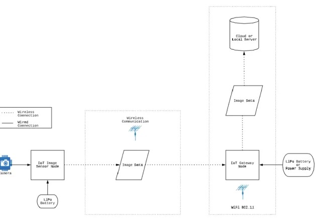
Figure 2: Typical IoT Network Structure
The general flow of data is: (1) data collection by Sensor Nodes, ranging from temperature data to image data, (2) data transmission over an RF communication link from Sensor Nodes to Gateway Nodes, (3) Gateway Nodes store data and upload previously collected data to Cloud Servers via the internet, and (4) easily accessible storage of data in the Cloud Server to be utilized by the end user from anywhere in the world with an internet connection.
As a summary of important parts of an IoT network, the following list defines key terms.
• Sensor Node – Performs data collection and storage, has ability to receive and transmit data over RF communication
• Gateway Node – Ability to receive and transmit data over RF communication, the internet access point, uploads received data via internet
• Cloud Server – Data storage on the internet, easily accessible via the internet from anywhere, at any time for the end user
1.4 Scope of Work
This thesis provides design and development decisions in creating a low-cost, low-power IoT system to be used in agricultural applications. This research will aim to build a standalone prototype system with the ability to be expanded upon. The main goal for the prototype system is to develop essential
all three. As the prototype sensor node will be designed to monitor crops, the device lifetime should be at least 1-year of uninterrupted operation on battery power. Each node in the network should cost no more than $30 to enable affordable implementation for farmers. The end user of the image data should be able to access captured pictures at any time via the internet.
Chapter 2 reviews relevant research papers pertaining to similar IoT systems developed. Chapter 3 reviews a preliminary system design for this thesis while providing specific goals and hardware case studies. Chapter 4 overviews the hardware system chosen for this thesis, the ArduCAM IoTai, and details features of the development board as well the core SoC, the ESP32. Chapter 5 documents design decisions and processes while developing key features of the IoT system. Chapter 6 details a comprehensive
Chapter 2 LITERATURE REVIEW
This chapter discusses three previous papers or projects that have developed IoT systems in agricultural settings. The goal of this literature and project review is to gain an understanding of what designs and decisions were made to develop successful similar systems in the past and learn from them. While none of the works reviewed here tackled the specific task of capturing and connecting image data to the internet, they do contain valuable information regarding wireless communication and unique hardware solutions. In fact, the task of agricultural IoT imaging for the purpose of crop detection and yield prediction (albeit a very narrow topic) seems to have never been attempted before.
2.1 Vinduino
2.1.1 Overview
The first project was born out of necessity by a California farmer. Vinduino (Vineyard + Arduino), was created to better manage the irrigation system of a southern California vineyard. The primary goal of the system was to provide a low-cost and easy to build system with rugged components for optimizing agricultural irrigation.
The process of the system developed is depicted in the Figure 3. The sensor nodes are placed out in the fields where they can collect any needed data from crops. They then send the collected data out to the gateway node, placed near the edge of the field and close to an internet router. This gateway can then upload the data via the router to a cloud server, where the data is aggregated into graphs to be easily analyzed by the farmer. After checking the data, the farmer can then send out simple commands to the sensor nodes to change irrigation control, if needed.
Figure 4: Vinduino Remote Sensor Node [6]
The project uses multiple soil moisture sensors, located at different depths to prevent overwatering and control irrigation to not exceed the active root zone. The solar powered remote sensor nodes have three gypsum soil moisture sensors and several options for temperature or humidity sensors. The designed board, shown in Figure 4, includes a Globalsat LM-210 LoRa module for long-range wireless communication (up to 6 miles), a built-in solar battery charger, and a built-in real time clock (RTC) for precise irrigation timing. This board also has the option to plug in an ESP8266 SoC to provide Wi-Fi connectivity. The functionality of the sensor node is controlled by an Arduino Pro Mini [6].
This platform service is made by MathWorks, the makers of MATLAB. ThingSpeak allows data to be aggregated, visualized, and analyzed in real-time in the cloud, shown in Figure 5.
Figure 5: ThingSpeak (by MathWorks) Analytics Platform
Any data that has been uploaded to ThingSpeak can be processed and analyzed in MATLAB. The farmer can view this data from wherever he wants with an internet connection on his own personal machine. With these visualizations, he can make decisions about irrigation and send simple commands to the irrigation valves via the sensor nodes to adapt to any changes.
2.1.2 Analysis
While this previous work was not an academic paper, it provides an incredible amount of information and documentation on its development, which is why I chose to include it in this thesis. This project saw real-world success and was completely implemented in this farmer’s vineyard. The success of this project’s functionality should not shield it from a critical review and analysis, though. This section will briefly overview what this project did well, and what could possibly be improved.
and ThingSpeak are intentional and gave me some insight into design tradeoffs including data rate, transmission distance, data size, and cloud platform limitations.
The sensor and gateway nodes in this project were designed and implemented with discrete modules on to a custom printed circuit board. In my opinion, the design of the sensor node has a redundancy that could be fixed, and the physical hardware placement could be given a second look. On the sensor node, the optional ESP8266 SoC is used only as a Wi-Fi replacement if the LoRa module was deemed unnecessary. By making the ESP8266 a permanent installment of the node and removing the Arduino Pro Mini, the node would become a lot easier to modify and just as easy to control. The SoC does indeed include native Wi-Fi, but also integrates a 32-bit Tensilica microprocessor. This processor has many more capabilities than an Arduino Atmega328 microcontroller, including lower power consumption, more peripheral interfaces, and a lower cost. You can even program and upload code to the ESP8266 from the Arduino IDE. In addition to this hardware replacement, an improvement to the physical layout of the system can be made. Looking at Figure 3 of the system flow, it would be advantageous to move the location of the gateway node to near the farmer’s house. The farmer can easily install an internet router in his home (if not installed already) and completely cut out the internet router on the opposite side of the field. This would reduce cost and time to the farmer.
2.2 Long-range & Self-powered IoT Devices for Agriculture & Aquaponics Based on Multi-hop Topology
2.2.1 Overview
This paper presented at the 2019 IEEE 5th World Forum on Internet of Things (WF-IoT) presents a prototype design of a long-range, self-powered IoT device for use in precision agriculture [7]. The IoT system presented is shown in Figure 6.
The system is designed to collect temperature, humidity, light, air pressure, soil acidity, and soil moisture data and transmit it back to an IoT server. The sensor nodes are designed with BMD-340 modules based on the nRF52480 microcontroller with an on-board antenna. The controller has Bluetooth 5 long-range support integrated into the chip. They use the bq25570 integrated circuit from Texas Instruments for energy harvesting, battery charging, and voltage conditioning. The nodes are powered from a Li-Ion battery with a 120mAh capacity. The sensor nodes are programmed to transmit at 125 kilobits per second in long-range mode using forward error correction (FEC) scheme to perform error detection and correction on received data.
To transmit this data collected at the sensor nodes to the gateway node, based on the ESP32 SoC, a custom developed “multi-hop” network is used. This network allows the system to extend its range to full coverage of large crop fields. The protocol enabled data transmission distances of 1.8km per hop, extending sensor coverage of almost any size to be viable. As this system will have many sensor nodes and a few gateway nodes placed around a large field, this network topology is able to route messages towards a dedicated gateway, where the closest gateway is chosen after the network has adapted. Once data gets to a gateway node, the messages are published via MQTT over Wi-Fi to a local network server.
2.2.2 Analysis
2.3 Smart Agriculture Farming with Image Capturing Module
2.3.1 Overview
This research paper, submitted to the 2019 Global Conference for Advancement in Technology (GCAT), focuses on the development of building an IoT system with a camera module device to analyze possible diseased crops [8]. The scope of this paper is similar to this one but aims to solve a different agricultural problem.
Figure 7: Block Diagram of IoT System Implementation [8]
The architecture of the system is given in Figure 7. An Arduino Mega 2560 acts as the central processor and initiates all tasks in the process. The model uses temperature, humidity, and water moisture sensors connected to the analog pins of the Arduino as well as an OV7670 0.3-megapixel camera. Data collected by the system is received by the Arduino and sent to the cloud using an ESP8266 as a Wi-Fi module.
The team used Firebase (backed by Google) as cloud storage for all data collected by the device. Firebase is a user-friendly platform to create and use databases for dynamic storage. The data can then be accessed by anyone with the proper authentication from any internet connected device. Figure 8 shows the synchronization of data over any connected device.
2.3.2 Analysis
Chapter 3
PRELIMINARY SYSTEM DESIGN
3.1 System Goals
The proposed system will be the sole data collection step in this CV and ML pipeline and focus on creating a base functionality design that can be its own standalone point-to-point system able to monitor the growth of a single viewable area in a farm. The goal of this thesis is to develop a low-cost, low-power image acquisition IoT solution that addresses the common issues seen by previous works.
In order to create a good solution, the development focused on the following areas.
• Low Cost: The designed system should be affordable for the end user and consumer. Each node should be at most $30.
• Low Power: The system (especially the sensor node) should use as little power as possible. The nodes must have long lifetimes while running on battery power. The longer the devices can run on a single battery charge, the less frequent they have to be maintained by a human. The sensor nodes should last at least 1-year operating on battery power.
• Scalability: While this thesis aims to develop a single sensor node and gateway node pair with accompanying significant functionality, this network will likely have to expand in size to meet farmer demands. A focus should be put on scale so that the network is easily able to accommodate change and improvement down the line, such as a mesh network.
• Autonomy: This system should be primarily autonomous to reduce the amount of effort by humans to collect and utilize this image data. Once this system is in place, no human input or maintenance will be needed until the battery is discharged.
Figure 9: Preliminary High-Level System Design
The decisions now must be made on what hardware will be used as the sensor and gateway nodes, which wireless communication technology will be used to link the nodes, and the best peripherals to be connected before we start functional development.
The two most significant factors to this design are the hardware/software ecosystem and the wireless communication technologies chosen. These two things will facilitate data flow and data speeds throughout the system. The following two sections will describe the needs of the system with respect to each factor and compare different technologies reviewed.
3.2 Wireless Communication
Choosing the best communication method for sensor to gateway node links as well as the gateway link to the internet is significant. IoT systems generally have three different categories of wireless
3.2.1 LPWAN: LoRa and SigFox
The LoRa (Long Range) communication technology is a commonly used IoT protocol. This technology was the driving link for the Vinduino project, described in Chapter 2. LoRa is a low-power wide-area network technology. It is based on spread spectrum modulation techniques and uses license-free sub-gigahertz radio frequency bands like 433MHz or 915MHz. This enables very long-range transmissions with low power consumption. While LoRa has a line-of-sight range of multiple kilometers, it has incredibly low bandwidth. This puts significant limitations on the data that is can be sent. The message payload needs to be as small as possible and encoded as binary data. Most recommendations keep the payload under 12 bytes. Because the data has to be transmitted over such a long distance, the interval between messages should be in the range of several minutes [10]–[13].
SigFox is a very similar communication technology as LoRa. The technology operates in the license-free frequency bands around 920MHz. It is a lightweight protocol with very little overhead needed to transmit data which means it consumes very little power. SigFox only supports one-way communication as opposed to the bidirectionality of LoRa. The pitfalls of SigFox follow those of LoRa. The communication technology is ultra-narrowband and will only support 140 messages per day per device with 12 byte payloads [14], [15].
While both LPWAN technologies have their advantages in most classic IoT networks, their biggest limitation is the largest disadvantage for our system. In order to create low-power sensor nodes for this imaging system, the transmission time must be minimized. To do this, the communication bandwidth must be large, and the data rate must be fast enough to transmit kilobyte sized images in a reasonable amount of time.
3.2.2 PAN: ZigBee and Bluetooth Low Energy
The wireless standard known as Bluetooth should sound familiar to most people. It describes a short-range wireless communication technology that has penetrated the consumer market faster than any other. The Bluetooth Special Interest Group introduced Bluetooth Low Energy, a newer standard than the classic serial port profile (SPP) Bluetooth, and this now has monopoly over the consumer electronic short-range communication market. It is used in almost every device people use on a day to day basis and has become synonymous with in-home IoT solutions. BLE has a slightly shorter range than ZigBee, but also has a much higher data rate at around 1 megabit per second for short bursts. The low energy aspects come when the device sleeps in between those bursts, which requires less power usage. ZigBee does not have this functionality [16], [17]. BLE also has the ability to be configured in a mesh or star network topology, giving it scalability for variable size networks.
As the idea for a large IoT network has potential for the system being developed, these PAN
technologies are an attractive option. The number of sensor nodes will most likely be large and constrained to a relatively small area, so the distance between these nodes will be small. This enables the use of such communication technologies.
3.2.3 Summary of Wireless Communication Technologies
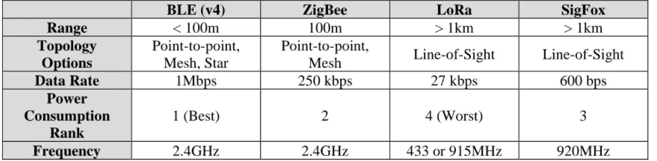
Table 1 describes the four communication technologies discussed while comparing certain key characteristics between them.
Table 1: Wireless IoT Communications Comparison
BLE (v4) ZigBee LoRa SigFox
Range < 100m 100m > 1km > 1km
Topology Options
Point-to-point, Mesh, Star
Point-to-point,
Mesh Line-of-Sight Line-of-Sight
Data Rate 1Mbps 250 kbps 27 kbps 600 bps
Power Consumption
Rank
1 (Best) 2 4 (Worst) 3
Frequency 2.4GHz 2.4GHz 433 or 915MHz 920MHz
3.3 Hardware Case Studies
This section briefly outlines the core hardware that was assessed to develop this IoT system. Hardware solutions were researched after deciding that BLE would be the wireless communication to transmit data from sensors to gateway nodes. Key characteristics in attractive hardware were various low-power modes, integrated BLE modules, numerous peripheral selections, and cost.
3.3.1 Arduino Nano 33 BLE
The Arduino Nano 33 BLE features a powerful nRF52840 32-bit ARM Cortex M4 processor that runs at 64 MHz. The board has 1 MB of program memory and 256 kB of SRAM [18]. Figure 10 shows the physical development board.
Figure 10: Arduino Nano 33 BLE Board [18]
The board also integrates 14 digital GPIO pins and one UART, SPI, and I2C interface each. The nRF52840 has a fully integrated Bluetooth 5 module with BLE mode. This chip is also able to run in multiple sleeping modes for low-power consumption in the microamp range.
3.3.2 Particle Argon
Figure 11: Particle Argon Development Board [19]
It has plenty of storage with 1 MB of program memory and 256 kB of RAM for the nRF52840 and 4 MB of program memory for the ESP32. There are 20 mixed signal GPIO lines with UART, I2C, and SPI interfaces. This system has only one PCB antenna (for BLE) but has two separate U.FL ports to attach external antennas for Wi-Fi and BLE [19].
3.3.3 Espressif ESP32 SoC
The ESP32 is advertised as a low-cost, low-power SoC with integrated Wi-Fi and Bluetooth 4.2 capabilities. At the core, there is a dual-core Tensilica Xtensa LX6 microprocessor that runs up to 240MHz. The ESP32 also integrates an ultra-low power co-processor and an RTC for low current consumption with five different sleep modes [20]. Figure 12 shows the surface mount chip that is soldered on to a variety of development boards.
Figure 12: Espressif ESP32 SoC
3.3.4 Hardware Summary
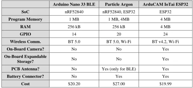
Table 2 summarizes key points in the hardware solutions reviewed. The characteristics chosen are of importance to the specific IoT system being developed in this thesis.
Table 2: Hardware Features Summary
Arduino Nano 33 BLE Particle Argon ArduCAM IoTai ESP32
SoC nRF52840 nRF52840, ESP32 ESP32
Program Memory 1 MB 1 MB, 4MB 4 MB
RAM 256 kB 256 kB 4 MB
GPIO 14 20 24
Wireless Comm. BT 5.0 BT 5.0, Wi-Fi BT v4.2, Wi-Fi
On-Board Camera? No No Yes
On-Board Expandable
Storage? No No Yes
PCB Antenna? No Yes (only for BLE) Yes
Battery Connector? No Yes Yes
Cost $20.20 $27.00 $19.99
While all of these platforms have the potential to develop into an IoT system, the cost of the platform is a major selling point. The Arduino and Argon board are feature-rich solutions but would require external purchasing of cameras and expandable storage hardware to be used, adding to the prices listed. The ArduCAM IoTai based on the ESP32 provides a wide array of scalable features and integrates all the wanted peripherals onto a single development board for under $20. For these reasons, the ESP32 based ArduCAM IoTai is chosen to be at the heart of the proposed IoT system.
3.4 Final Design Summary
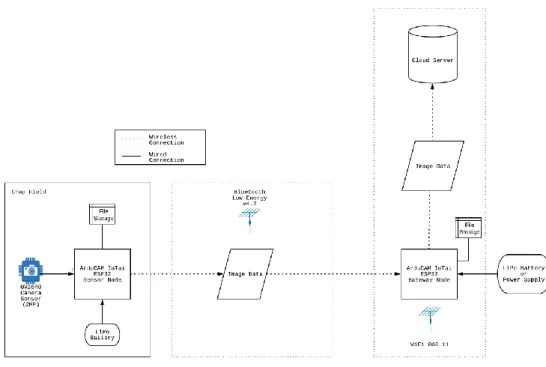
Since the gateway node will be assumed to be near a stable internet connection, it will also be assumed it will be near a constant power source. This description is illustrated in Figure 13 below.
Chapter 4
HARDWARE OVERVIEW
This chapter will give an overview of the hardware chosen for the development of this thesis. A detailed discussion of the features of the ArduCAM development board, ESP32 system on a chip (SoC), and OV2640 image sensor module will be included, as these are the primary pieces of the IoT system being developed.
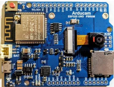
4.1 ArduCAM IoTai Development Board
The device chosen to function as both the sensor node and gateway node in our network is the ArduCAM IoTai UNO PSRAM development board, shown in Figure 14. This hardware module is an all-in-one solution with many attractive features for developing a custom IoT system.
Figure 14: ArduCAM IoTai Development Board
This development board is based on the ESP32 SoC and the OV2640 2 Megapixel Camera Module, which are both described later in this chapter. Apart from these two components, the development board also features the following useful parts:
• MicroSD Card Slot
• LiPo Batter Connector (2-pin)
• 4MB PSRAM, 32Mbit Flash
• USB-Serial Interface
The microSD card slot and plentiful on-board flash storage are large factors in making this system a scalable network. Having the option to be able to variably expand the on-board storage of this board allows for greater flexibility in its applications. MicroSD cards are sold with a wide range of storage sizes, from 64MB to 512GB, depending on the type of card. The flash storage chips also give a way to organize image files well due to the fact that a basic tree file system can be implemented on them rather easily. Because our application will be based around the storage of images that will vary in size, it is important to have plenty of storage space on these devices as well as a good organization system to easily access the image files in software.
The development board features a 2-pin battery connector to power the system. The sensor node of the proposed system will be far away from any power sources, so it must be powered by a battery. This connector leads to a voltage regulator that will power the ESP32 SoC at 3.3 volts, therefore, we can have batteries of different nominal voltages plugged in to our development board, expanding our options.
Program memory is incredibly important in this design. Apart from storing images, the board must be able to store firmware and its overhead. With 32Mbits of flash memory, the board can store a respectable amount of firmware, and with 4MB of PSRAM (pseudo-static random-access memory) it can create and manipulate significant amounts of program variables when firmware runs. For a comparison, an Arduino UNO based on the ATmega328 chip has 32kB of flash memory and 2kB of SRAM (static RAM) memory. Our system will need a significant amount of memory for programs and variables as the system will be using Wi-Fi and Bluetooth technologies which include large overhead sizes for controllers and other needed data.
Though it is not necessarily a requirement for programming, the board features a USB-serial chip that makes program compilation and uploading very simple. The alternative to this would be to use an FTDI adapter which allows for many common problems to occur when trying to program the board, like improper wiring or compatibility issues.
Lastly, the development board includes a PCB antenna for radio frequency (RF) transmissions from the ESP32, as well as a U.FL connector for the option to attach an external antenna. This feature is
4.2 Espressif ESP32 SoC
The most important part of the development board is the SoC it is built around, the brains of the system. The ESP32, created by Espressif Systems, is a low-cost, low-power system with both Wi-Fi and dual-mode Bluetooth capabilities. At its heart, the chip features a dual-core Tensilica Xtensa LX6
microprocessor with a clock frequency of 240MHz. Designed for mobile devices and IoT applications, the ESP32 achieves ultra-low power consumption through multiple power saving features and relying on its real-time clock (RTC) and ultra-low power co-processor (ULP). The full functional block diagram is shown in Figure 15.
Figure 15: ESP32 High Level Functional Block Diagram [20]
The ESP32 also features many interfaces for the addition of peripheral devices. These include standard I2C (inter-integrated circuit), DAC (digital-to-analog converter), SPI (serial peripheral interface), and SDIO (secure digital input output). All of these interfaces are incredibly important for designing a scalable IoT system that can adapt to changes and additions. Though this thesis will not include any external devices that need to be directly interfaced with (like analog sensors), having the option and bandwidth to do so is a large advantage for this system.
4.3 OV2640 Image Sensor
This system being developed relies on images, so the camera module used is of great importance. The module must be able to capture quality images and have the ability to control many image processing functions like white-balancing, saturation, de-noising, and similar processes.
The OV2640 camera module is a low voltage CMOS image sensor that provides full functionality of a single-chip camera and image processor in a small package. This module is included with purchase of the ArduCAM development board, though it is possible to replace this camera with another parallel interface image sensor if necessary. The physical module is depicted in Figure 16.
Figure 16: OV2640 CMOS Image Sensor Module [22]
This 2-megapixel camera module is capable of UXGA (ultra-extended graphics display) image display mode where the resolution of a captured image is 1600 pixels horizontally by 1200 pixels vertically (1600x1200). This totals 1.92 million pixels on the display. For our agricultural imaging application, this image quality is sufficient. If better image quality is needed at later time, a higher quality parallel interface camera module can be purchased separately and used with this system.
A very important aspect of this module is the fact that it features an on-chip compression engine. This engine consists of three major blocks: a DCT (discrete cosine transform) block, a quantization block, and an entropy encoding block (Huffman encoding) [22]. These three blocks perform JPEG compression on images captured, greatly reducing the size needed to represent and store the image while keeping the image quality almost unchanged. Reducing the size of these images will decrease the amount of time it takes to transmit the image data, therefore decreasing the amount of power being used by the system. This will allow for a longer device lifetime while running on battery power.
white-balance, and black-level calibration. Exposure is the amount of time the CMOS sensor array is exposed to light; gain controls the amplifier gain following sample and hold circuitry; white-balance control removes unrealistic color casts so that objects that appear white in person are rendered white in the image; black-level calibration refers to the brightness of the images making sure they do not seem too dark. This feature-packed camera module includes everything needed to be a robust image capture module for our IoT system.
4.4 Other Considerations
One important aspect of this system is keeping it affordable to the end user or consumer. All the hardware described in this chapter was purchased in one package, available from ArduCAM’s website. The price for both the ArduCAM IoTai development board and OV2640 camera was $20. This price for the amount of hardware potential is impressive. While the development board with integrated peripherals was bought for this work to more easily develop primary base functionality of an IoT system, the core pieces of this can be cheaply bought individually or in smaller packages if simpler sensor nodes without imaging capabilities are needed.
Figure 17: ESP32-DevKitC Breakout Board
Chapter 5 DEVELOPMENT
5.1 Functionality Overview
This chapter describes the chronological development of significant functions within the IoT system. Each section discusses how a specific system function was created in code and attempts to explain why certain decisions were made in reference to the system goals and requirements. The following topics are presented: the embedded environment used to develop firmware, image capture processes for the sensor node, two viable storage options and respective interfacing, BLE theory, ESP32 BLE functionality for sensor and gateway nodes, low-power sleep modes for the sensor node, and Wi-Fi connection to the Firebase cloud on the ESP32.
5.2 Embedded Development Environment
The firmware developed and tested in this thesis was written in the Arduino Integrated Development Environment (IDE). This environment was chosen as it has the least number of obstacles to begin using and understanding. The Espressif ESP-IDE is also a viable choice for the more experienced embedded
developer but has a steeper learning curve than the Arduino IDE. The Arduino IDE is a familiar software environment for anyone who has tinkered with the open-source hardware platforms Arduino provides. The environment is incredibly popular around the globe and has a significant developer community behind it. This means there are many forums, tutorials, and assistance available to get started developing with this IDE.
The Arduino IDE does not come with the ability to interact with the ESP32 SoC or ArduCAM development board automatically. Luckily, there is an easy way to install the board and processor
Figure 18: Additional Board Manager URL Field
Enter the file URL into the field shown in Figure 18, separating multiple URL’s with commas. This file contains all the necessary links and tools to use all the features on the ArduCAM board. After this is entered, the ESP32 platform package must be installed in the “Boards Manager” menu, found at Tools->Boards->Boards Manager.
Figure 19: ESP32 Platform to Install on Board Manager
https://github.com/ArduCAM/ArduCAM_ESP32S_UNO_PSRAM. The site has many C and C++ source and header files for drivers and API’s to make interacting with the development board electronics a little easier.
5.3 Image Capture – Sensor Node
The first function to test and implement is to capture an image using the OV2640 camera module, as the entire IoT system revolves around this visual sensing functionality. The goal is to efficiently capture quality images to be used in computer vision processes down-the-line. To develop this, a few files are especially helpful: esp_camera.h, arducam_esp32s_camera.h, sensor.h. The first file provides a camera configuration structure as well as a data structure for the camera frame buffer. The second defines specific API function calls for camera initialization and other key actions. The third provides structure of the OV2640 driver and different settings available to the image sensor.
The basic idea of the function flow is depicted in Figure 20 below. After powering up and booting the processor, we must detect and initialize the camera module to be sure it is ready and capable to capture an image. Once the image is captured, we must provide pointers to the image frame buffer and the image frame length (or size). The buffer will hold the entirety of the image data while the frame length holds the size of the image, in bytes. These two pieces of information will be necessary in storing the imagen in either flash storage or a microSD card. A boolean flag “ESP_OK” is also returned to represent the success or failure of capturing an image.
Figure 20: Image Capture Firmware Flow
holding GPIO pin numbers for camera lines, clock frequency and timing channels, pixel format, and frame size information. This function returns a success flag if the initialization operations are completed.
Figure 21: API Function Names with Parameters
The camera sensor has a control structure defined in sensor.h that can be obtained by using the second function in Figure 21. With this structure, we gain the ability to vary and set different sensor actions while the camera is already initialized. These include brightness, contrast, frame size, gain controls, and many more.
The third function captures an image by obtaining a pointer to the frame buffer that holds the entirety of the image data. The frame buffer data structure contains five variables: a buffer, length, width, height, and format. The combination of these fully describe the image.
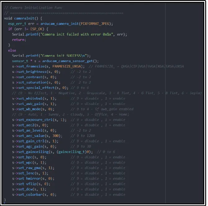
Figure 22: Camera Initialization Custom Function
shown in the function are done entirely on the OV2640 image processor. The effects and the chosen values are what produced the best images, but the comments describe possible input options. Most image effects are set to be automatic.
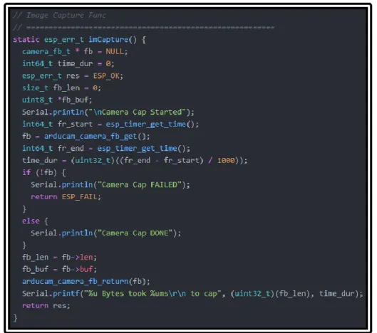
Figure 23: Image Capture Custom Function
An image capture function was developed around the API functions for our specific purposes, seen in Figure 23. Appropriately sized variables are initialized as null or zero valued for the frame buffer
At this point the image capture function is almost complete. The length and buffer data attributes must be either stored on the device for transmission later on or immediately transmitted off the device. The decision to store the image data on the device for future transmission is made for a few reasons. First, the system being developed must be as scalable as possible. As more imaging nodes are added to the system, a device may not be able to immediately transmit, or the recipient may not be ready to receive data, so organized immediate storage is the best option. This is where either flash or microSD storage can be used. The development of the remaining camera functionality is done without a final decision between these two storage options. The code needed to interact with both storage options is essentially the same with the use of the serial peripheral interface flash file system (SPIFFS) and the SD card file system libraries. The implementation of both is shown in the following section. A more in-depth comparison of the two storage types can be found in Chapter 6.
5.4 SD Card and Flash Storage Interface
5.4.1 SanDisk Industrial 8GB Card
The microSD card chosen for this work is the SanDisk Industrial 8GB card. This is a popular card chosen primarily for its low price and industrial specifications. Commercial microSD cards (regardless of manufacturer) have an operating temperature range of about 0 to 70°C (or 32 to 158°F for us Americans). The limiting factor is the low end of the temperature range as our application of this device is in crop fields where it can easily get below freezing, especially in the winter. The industrial grade cards produced by SanDisk are ideal for this application. The operating temperature range of the card being used is -25 to 85°C [25]. This range includes any temperature we would expect to see crop fields to possibly exist in. Unfortunately, this industrial grade card comes at a higher price tag. An 8GB Industrial card can be bought for around $9 while the commercial counterpart is priced around $5.
5.4.2 Image File Reading and Writing
header files are drivers for the ESP32 to interact with the on-board microSD card reader and the on-board flash storage.
Figure 24: Image Data File Writing Code
The code in Figure 24 shows the basic idea of taking the previously gathered image data and writing it to a file on the microSD card. The PATH_NAME will include the path directory with the wanted file name (for example: /ArduCAM/image_number.jpg). Directories on the card can be made manually with a file explorer on a PC or in code using the SD_MMC.mkdir(). Directories can only be made in flash memory using the SPIFFS.mkdir() call.
Using this functionality, the image data can be stored on the microSD card or in flash. Initially, a single capture was taken and sent to the SD card in order to easily view the image on a PC. The resulting image was surprising. It was dark and had bad white balance showing a green tint. Originally, the thought was that the automatic settings would do a better job at correcting the image. After some testing, it was found that the images would look best if they were taken in series of around five at a time, where the quality of the image increased until image three. After the third image, the pictures would look balanced and well corrected. This increase in quality of images from the first to the last image in one series of five is shown in the Figure 25.
Figure 25: First through Fifth Image Taken in Series with OV2640
consistently save and transmit the best image available. Therefore, it is best to take image captures in series of at least five and save the last one to storage for transmission.
Figure 26: Image Captured by OV2640 (rotated 90 degrees), 139KB
Figure 26 shows an image captured with a textbook in view. This shows the color saturation, brightness, and balance are all sufficient using the automatic settings. It is an impressive image for a 2-megapixel simple camera module. The 1600 by 1200 pixel image file is compressed to 139KB by the JPEG engine, a compression ratio of almost 14.
Theoretically, the 8GB microSD card could hold over 57,000 equivalent images. While this seems like an impractical metric for the point-to-point system being developed for this work, the system needs to be scalable. This large storage space would allow for many sensor nodes to save and share image data between themselves frequently before finally routing the image to the gateway. This also allows space for other types of data along with images to be saved. Prediction systems in the future will likely need more than just image data to be robust. The ability to save other data types like temperature, soil moisture, and airflow data could prove useful.
has been transferred off the device, the file can be removed as it is no longer needed. By constantly transmitting and subsequently removing image files, flash storage is still a viable storage option.
Though the microSD storage seems much better for our system at this point due to its easily
expandable memory, a disadvantage is mentioned in the following section. The use of flash storage also has a major advantage compared to a microSD card in terms of power, discussed in chapter 6.
5.4.3 Challenges
Using the microSD card for storing images on this development board poses an interesting problem that came up while monitoring system current draw. Surprisingly, microSD cards are actually very power-hungry devices. They require large currents to read and write data, up to 100mA for the SanDisk being used [23]. These read and write times are relatively short compared to the amount of time the card will sit idle and unused. Unfortunately, the idle current draw for this type of storage device is around 500µA, constantly pulled when unused. While this current value sounds small, the sensor node will spend the vast majority of its operational lifetime trying to use as little current as possible to extend battery life. The development board has a dedicated voltage regulator for the microSD card reader, meaning the card will continuously be powered even when the ESP32 is in a low-power mode. This problem is addressed in more detail in Chapter 6.
5.5 Bluetooth Low Energy (BLE) Functionality
5.5.1 BLE Theory and Overview
In order to develop firmware that follows the Bluetooth Low Energy standard, one must understand basic theory and operation of the wireless communication. BLE is often the ideal choice for devices that want to send small amounts of sensor data while using minimal power over short distances. Our use-case of BLE is slightly unusual, as we want to transmit relatively large image files in infrequent bursts. The primary reason we are using BLE rather than classic Bluetooth is because of the flexibility in network topologies. BLE supports point-to-point, broadcast, and mesh topologies while the classic only supports the first. BLE is chosen to make this system as scalable and adaptable as possible for the future.
device that wants to receive this data. Figure 27 below depicts the two types of devices within BLE and the connections between them.
Figure 27: BLE Basic Server and Client Interaction
When the server has control of the data it wants to share over the air, it can “advertise” its existence to clients that happen to be in the general vicinity. A client can “scan” the area and attempt to find a
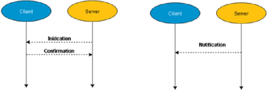
connection to a server in order to receive data. Once a verified connection is made, the server can proceed in one of two directions. One is to send data without letting the client know, forcing the client to poll for data. The other is for the server to immediately update the client when it sends data using either
“notifications” or “indications,” both of which are shown in Figure 28.
Figure 28: Indication / Notification Schemes
Now, how does each device know which other devices it should connect to? And what is the data format for packets that are being transmitted? Both of these questions can be answered by studying the Generic Attribute (GATT) hierarchical data structure that sits on top of the BLE layers, depicted in Figure 29. This structure defines basic models and procedures to allow devices to discover, read, write, and push data elements between them [24]. This is important to understand as it will help us use BLE and write our firmware.
Figure 29: GATT Data Structure for BLE [25]
The topmost layer of this data structure is the Profile, which technically does not exist on the actual BLE peripheral itself, the ESP32 in this case. The Profile is a pre-defined collection of Services that have been compiled by either the Bluetooth SIG or by other designers.
BLE Services are used to break up data being held into logic entities. They hold specific chunks of data called Characteristics (Services can contain more than one). Each Service is able to distinguish itself from others by using a unique numeric identification number, called a UUID. These identification numbers can either be officially adopted 16-bit values or completely custom 128-bit values. An example of this is the officially adopted Heart Rate Service (UUID: 0x180D) which contains three Characteristics: Heart Rate Measurement, Body Sensor Location, and Heart Rate Control Point. These are commonly used in medical or fitness wearable devices, like Fitbit watches.
understand this data. The Characteristic value is the main field that will interact with the BLE client and server; it is able to be written to and read from. The value has no restrictions on the type of data it can contain but is limited to 23 bytes of payload data, defined by the GATT structure maximum transmission unit (MTU) [26].
While this background does not make up all the theory or information that goes into BLE procedures and protocols, it is enough to understand the development procedure used in this thesis. New terms and concepts that are used and not mentioned above will be explained as they are brought up.
5.5.2 Image Transmission via BLE – Sensor Node
The development of a custom BLE image transmission process for the ESP32 involved reading and understanding many source and header C files within the BLE library in GitHub, in addition to the theory described in the previous section. The library source files can be located at:
https://github.com/espressif/arduino-esp32/tree/master/libraries/BLE/src. The Espressif API online manual also provides documentation of functions used within the library files for the Arduino ESP32 core.
5.5.2.1 General Overview
The firmware flow diagram in the Figure 30 depicts the high-level process of BLE image data transmission from the time of boot up and assumes there exists a specific image file we want to transmit. After capturing an image and saving it to storage, the process starts by defining the custom Service and Characteristic UUID values. Then the server is initialized as a BLE device, creates the Service and Characteristic properties, then begins to advertise itself over-the-air. It continues advertising until a stable connection is made to the correct client. Once this occurs, the storage file system is checked to see if the file we want to transmit exists. If it does, we open the file for reading. While we can still read new data from the file, we enter a custom algorithm that fills a buffer of any size (MTU less than or equal to 23 bytes) for any size image captured. Each time the buffer is completely filled, the Characteristic value is set before a BLE notification is sent, until the end of the file is reached. The process ends with the
Figure 30: BLE Data Transmission Firmware Flow Diagram 5.5.2.2 BLE Device Creation and Advertising on ESP32
To define the UUID’s for both the Service and Characteristic, we use a custom UUID generator from https://www.uuidgenerator.net. The values generated by this site for the Service and Characteristic UUID values respectively are:
Next, the actual BLE device instance is created with a name of our choice; “ESP32” is chosen for simplicity. This is the name that will be displayed for other devices to view it. The BLE server, Service, and Characteristic with all properties are then created. Figure 31 shows the code to instantiate these. The properties chosen to be included with the Characteristic are READ, WRITE, NOTIFY, and INDICATE. These are all properties that can be enabled but do not necessarily all have to be used for a specific case.
Figure 31: Creation of BLE Device, Server, Service, and Characteristic
Figure 32: Start BLE Advertising
Once advertising has started, we must determine when our specific client has found our server and when it has made a complete connection. In order to do this, we use a callback function. After the creation of the Server, we can add in a line of code to set its callback as a custom function we name
MyServerCallbacks(). This callback function is only triggered or entered when the Server connects to a client successfully. So, when the Server and Client make that stable connection (or disconnection), we are able to write any code to run as soon as this happens. To separate the connection and disconnection alert actions, we define two different custom functions within the MyServerCallbacks, OnDisconnect() and OnConnect(). Inside the connection function, we set a Boolean flag called deviceConnected to true. This flag enables code to run that will format and transmit chunks of image data.
5.5.2.3 BLE Data Format and Transmission on ESP32
The code developed to format and transmit the data sits within an adaptive buffer filling process. Figure 33 shows a detailed flow of the firmware developed to format and transmit image data. As a
Figure 33: Data Formatting and Transmission Firmware Flow
First, the device must decide it is ready to transmit to a client by checking the connection status. If the deviceConnected flag is true and the Tx_DONE flag is false, we enter our first statement. Once inside this conditional, we initialize the storage file system and check to see if a file exists that is ready to be
remainder of the file size divided by the MTU, chunkSize. This operation is done using the modulo operator. If the result is not zero, that means the final buffer transmission will be unequal to the MTU size. This result will vary between every image capture and is stored in a variable called remSize. Next, we want to continually read the image data and format buffers until the end of the file. To do this, we use a file system method called “available.” This method checks to see how many bytes are available for reading from the file and returns zero when it is at the last byte of data in the file. Depending on the result of remSize, we enter one of two case statements to continuously fill buffers, write Characteristic values, and send notifications to the client device so it is aware of new data. To set BLE data values and send a notification, Figure 34 shows the two lines of code that are used.
Figure 34: BLE Characteristic Value Setting and Notification Code
The only time the new buffer size determined by remSize is utilized is just before the last notification is sent for the last data packet transmission. Once the image file has been transmitted, we set the Tx_DONE flag, close the file, de-initialize the storage system, and de-initialize the Bluetooth controller on the ESP32. This stops all processes required to operate these functions on the CPU and most importantly stops the power-hungry BLE RF hardware.
This entire described process is best illustrated through an example. Figure 35 and Figure 36 display the serial port while the device is running, and the printed statements show what is taking place. During this example, the chunkSize was set to 4 bytes of image data.
In Figure 35, a series of five images are captured and the advertising period is started. Once a connection is made to the client, the sizes are printed of the file to be transmitted, the current MTU size, and the remSize. Because the file size (61600 Bytes) was perfectly divisible by the MTU (4 Bytes), case 1 is entered, and the image file is transmitted using a single size buffer.
Figure 36: Case 2 Process in Serial Port
In Figure 36, a different series of five images are captured. This time, however, the file size (61017 Bytes) is not divisible by the MTU (4 Bytes). There is one byte of data remaining, so the buffer structure must be of a different size and case 2 is entered. This process adjusts to any appropriately size MTU and any size image file to ensure full file transmission.
By changing the value of the MTU (chunkSize), we can enable higher data throughput for our system. When this code was initially tested with using a minimum chunkSize of one-byte, full image transmission typically took around one minute. This time duration must be minimized as wireless transmission has the highest power consumption out of all the CPU functions, so the MTU should be near or at the limit of 23 bytes. Chapter 6 discusses the optimization and analysis of this image data throughput.
5.5.3 Image Reception via BLE – Gateway Node
5.5.3.1 General Overview
5.5.3.2 BLE Client Testing with nRF Application
Initially, to test the functionality of the BLE server, the Nordic nRF android application was used on a smartphone. Instead of developing a client device on another ArduCAM development board and having to debug both sides at the same time, one can use this application to have their smartphone act as a client to view necessary BLE information. This method reduces the amount of debugging needed and provides a quick and efficient way of testing the server-side functionality. Once the nRF is installed and opened, navigate to the “Devices” section by tapping the 3 bars in the upper left-hand corner, shown on the left of Figure 37.
Figure 37: Nordic nRF BLE Connection Screenshots
This will take the user to the scanning page, where all BLE devices currently advertising within range will be listed, shown on the right of Figure 37. Each device will have a name (we called ours “ESP32” in our code) and if applicable, an option to connect to it. By connecting to our ESP32 device, we trigger our board to transmit image data, as written in our server code. nRF allows us to see the Service and
Figure 38: ESP32 BLE Device Information on nRF App
As shown in Figure 38, our device is “Unknown” because we have defined our device with custom UUID values. The values in both the Characteristic and Service UUID fields both match the values we configured in code. The Characteristic value shown (0x76-0x13-0x6E-0xDC) is a four-byte chunk of image data being transmitted at that instant in time.
This application allowed for easy debugging of BLE code being developed. The app was used incrementally during all steps of the Sensor Node development to ensure proper operation of code. nRF also gives a few other pieces of information that is useful to a developer, like the transmit power level and advertising interval. Using this method, the operation of the server side BLE firmware is confirmed.
5.5.3.3 BLE Client on ESP32
![Figure 15: ESP32 High Level Functional Block Diagram [20]](https://thumb-us.123doks.com/thumbv2/123dok_us/8220504.2179454/37.918.193.816.405.644/figure-esp-high-level-functional-block-diagram.webp)