VEML6075
www.vishay.com
Vishay Semiconductors
UVA and UVB Light Sensor with I
2
C Interface
DESCRIPTION
The VEML6075 senses UVA and UVB light and incorporates
photodiode, amplifiers, and analog / digital circuits into a
single chip using a CMOS process. When the UV sensor is
applied, it is able to detect UVA and UVB intensity to provide
a measure of the signal strength as well as allowing for UVI
measurement.
The VEML6075 provides excellent temperature compensation
capability for keeping the output stable under changing
temperature. VEML6075’s functionality is easily operated via
the simple command format of I
2C (SMBus compatible)
interface protocol. VEML6075’s operating voltage ranges
from 1.7 V to 3.6 V. VEML6075 is packaged in a lead (Pb)-free
4 pin OPLGA package which offers the best market-proven
reliability.
FEATURES
• Package type: surface mount
• Dimensions (L x W x H in mm): 2.0 x 1.25 x 1.0
• Integrated modules: ultraviolet sensor (UV), and
signal conditioning IC
• Converts solar UV light intensity to digital data
• Excellent UVA and UVB sensitivity
• Reliable performance of UV radiation
measurement under long time solar UV
exposure
• 16-bit resolution per channel
• UVA and UVB individual channel solution
• Low power consumption I
2C protocol (SMBus compatible)
interface
• Package: OPLGA
• Temperature compensation: -40 °C to +85 °C
• Output type: I
2C bus
• Operation voltage: 1.7 V to 3.6 V
• Material categorization: for definitions of compliance
please see
www.vishay.com/doc?99912
APPLICATIONS
• Handheld device
• Notebook
• Consumer device
• Industrial and medical application
Note
(1) Adjustable through I2C interface
Note
(1) MOQ: minimum order quantity
PRODUCT SUMMARY
PART NUMBER OPERATING VOLTAGE RANGE (V) I2C BUS VOLTAGE RANGE (V) PEAK SENSITIVITY UVA, UVB (nm) RANGE OF SPECTRAL BANDWIDTH UVB λ0.5 (nm) OUTPUT CODE VEML6075 1.7 to 3.6 1.7 to 3.6 365, 330 ± 10 16 bit, I2CORDERING INFORMATION
ORDERING CODE PACKAGING VOLUME (1) REMARKS
VEML6075
www.vishay.com
Vishay Semiconductors
Rev. 1.0, 18-Dec-15 Document Number: 84304
BLOCK DIAGRAM
Notes
(1) Nichia NCSU033X (365 nm) (2) UVTOP310TO39HS (315 nm)
ABSOLUTE MAXIMUM RATINGS
(T
amb= 25 °C, unless otherwise specified)
PARAMETER TEST CONDITION SYMBOL MIN. MAX. UNIT
Supply voltage VDD 0 3.6 V
Operation temperature range Tamb -40 +85 °C
Storage temperature range Tstg -40 +85 °C
RECOMMENDED OPERATING CONDITIONS (Tamb = 25 °C, unless otherwise specified)
PARAMETER TEST CONDITION SYMBOL MIN. MAX. UNIT
Supply voltage VDD 1.7 3.6 V
Operation temperature range Tamb -40 +85 °C
I2C bus operating frequency f
(I2CCLK) 10 400 kHz
PIN DESCRIPTIONS
PIN ASSIGNMENT SYMBOL TYPE FUNCTION
1 GND I Ground
2 SDAT I / O (open drain) I2C data bus data input / output
3 SCLK I I2C digital bus clock input
4 VDD I Power supply input
BASIC CHARACTERISTICS
(Tamb = 25 °C, unless otherwise specified)
PARAMETER TEST CONDITION SYMBOL MIN. TYP. MAX. UNIT
Supply operation voltage VDD 1.7 - 3.6 V
Supply current VDD = 1.8 V IDD - 480 - μA
I2C signal input Logic high V
DD = 3.3 V
VIH 1.5 -
-V
Logic low VIL - - 0.8
I2C signal input Logic high V
DD = 2.6 V
VIH 1.4 -
-V
Logic low VIL - - 0.6
Operating temperature Tamb -40 - +85 °C
Shutdown current Light condition = dark;
VDD = 1.8 V, Tamb = 25 °C IDD (SD) - 800 - nA
UVA sensitivity IT = 50 ms (1) - 0.93 - counts/μW/cm2
UVB sensitivity IT = 50 ms (2) - 2.1 - counts/μW/cm2
VDD SCL SDA GND
VEML6075
State machine 2IC interface
UV-PD
Oscillator
Timing controller
VDD
VEML6075 pin-out assignment
GND 1 VDD 4 SDAT 2 SCLK 3
VEML6075
www.vishay.com
Vishay Semiconductors
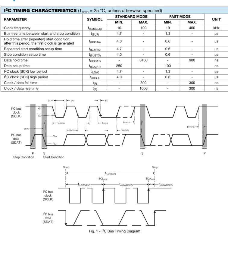
Fig. 1 - I2C Bus Timing Diagram
I
2C TIMING CHARACTERISTICS
(T
amb= 25 °C, unless otherwise specified)
PARAMETER SYMBOL STANDARD MODE FAST MODE UNIT
MIN. MAX. MIN. MAX.
Clock frequency f(SMBCLK) 10 100 10 400 kHz
Bus free time between start and stop condition t(BUF) 4.7 - 1.3 - μs
Hold time after (repeated) start condition;
after this period, the first clock is generated t(HDSTA) 4.0 - 0.6 - μs
Repeated start condition setup time t(SUSTA) 4.7 - 0.6 - μs
Stop condition setup time t(SUSTO) 4.0 - 0.6 - μs
Data hold time t(HDDAT) - 3450 - 900 ns
Data setup time t(SUDAT) 250 - 100 - ns
I2C clock (SCK) low period t
(LOW) 4.7 - 1.3 - μs
I2C clock (SCK) high period t
(HIGH) 4.0 - 0.6 - μs
Clock / data fall time t(F) - 300 - 300 ns
Clock / data rise time t(R) - 1000 - 300 ns
I2C bus clock (SCLK) VIH VIH t(LOW) VIL t(R) t(HDSTA) t(BUF) VIL t(HDDAT) t(F) t(HIGH) t(SUSTA) t(SUDAT) t(SUSTO)
{
{
P Stop Condition S Start Condition{
{
P S t(LOSEXT) t(LOWMEXT) t(LOWMEXT)SCLACK SDAACK
Start Stop t(LOWMEXT) I2C bus data (SDAT) I2C bus clock (SCLK) I2C bus data (SDAT)
VEML6075
www.vishay.com
Vishay Semiconductors
Rev. 1.0, 18-Dec-15 Document Number: 84304
PARAMETER TIMING INFORMATION
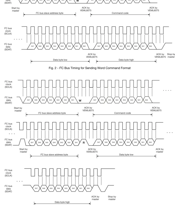
Fig. 2 - I2C Bus Timing for Sending Word Command Format
Fig. 3 - I2C Timing for Receive Word Command Format
ACK by VEML6075 ACK by VEML6075 ACK by VEML6075 ACK by VEML6075 I2C bus clock (SCLK) I2C bus data (SDAT) I2C bus clock (SCLK) I2C bus data (SDAT)
I2C busslave address byte Command code
Start by master
Stop by master
Data byte low Data byte high
SA7 SA6 SA5 SA4 SA3 SA2 SA1 SA7 SA6 SA5 SA4 SA3 SA2 SA1 SA0 SA7 SA6 SA5 SA4 SA3 SA2 SA1 SA0 SA7 SA6 SA5 SA4 SA3 SA2 SA1 SA0 W ACK by VEML6075 ACK by VEML6075 ACK by VEML6075 I2C bus clock (SCLK) I2C bus data (SDAT)
I2C bus slave address byte Command code Start by master SA7 SA6 SA5 SA4 SA3 SA2 SA1 W SA7 SA6 SA5 SA4 SA3 SA2 SA1 SA0 I2C bus clock (SCLK) I2C bus data (SDAT)
Data byte low
Data byte high
ACK by master Start by
master
I2C bus slave address byte
I2C bus clock (SCLK) I2C bus data (SDAT) ACK by master Stop by master SA7 SA6 SA5 SA4 SA3 SA2 SA1 R SA7 SA6 SA5 SA4 SA3 SA2 SA1 SA0 SA7 SA6 SA5 SA4 SA3 SA2 SA1 SA0
VEML6075
www.vishay.com
Vishay Semiconductors
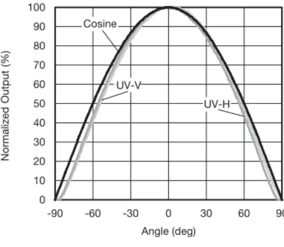
TYPICAL PERFORMANCE CHARACTERISTICS (Tamb = 25 °C, unless otherwise specified)
Fig. 4 - Normalized Spectral Response Fig. 5 - Normalized Output vs. View Angle
APPLICATION INFORMATION
Pin Connection with the Host
The configuration and data registers of the VEML6075 are accessed via the I
2C interface. The hardware schematic is shown
below in fig. 6.
The 0.1 μF capacitor near the V
DDpin is used for power supply noise rejection. The 2.2 k
Ω
is suitable for the pull high resistor
of I
2C.
Fig. 6 - Hardware Pin Connection Diagram
10 100 1000 10000 0 10 20 30 40 50 60 70 80 90 100 300 350 400 450 500 550 600 Axis Title 1 s t l ine 2nd line 2nd line N o rmal iz e d Output (%) λ- Wavelength (nm) 2nd line UVB UVA UVcomp2 UVcomp1 0 10 20 30 40 50 60 70 80 90 100 -90 -60 -30 0 30 60 90 Axis Title 2nd line N o rmal iz e d Output (%) Angle (deg) 2nd line Cosine UV-H UV-V 10 100 1000 10000 1 s t l ine 2nd l ine I2C bus data SDA I2C bus clock SCL SDA (2) SCL (3) GND (1) VDD (4) C1 100 nF 1.7 V to 3.6 V 1.7 V to 3.6 V R2 R1
Host
Micro Controller
VEML6075
VEML6075
www.vishay.com
Vishay Semiconductors
Rev. 1.0, 18-Dec-15 Document Number: 84304
Digital Interface
The VEML6075 contains a CONF register (00h) used for operation control and parameter setup. Measurement results are stored
in four separate registers, one each for UVA, UVD, UVB, UV
comp1, and UV
comp2(07h to 0Bh respectively). All registers are
accessible via I
2C communication. Fig. 7 shows the basic I
2C communication with the VEML6075. Each of the registers in the
VEML6075 are 16 bit wide, so 16 bit should be written when a write command is sent, and 16 bit should be read when a read
command is sent.
The built in I
2C interface is compatible with I
2C modes “standard” and “fast”: 100 kHz to 400 kHz
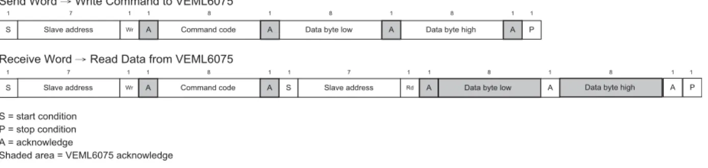
Fig. 7 - Command Protocol Format
Note
• Please note the repeat start condition when data is read from the sensor. A stop condition should not be sent here.
Slave Address and Function Description
VEML6075 uses 0x10 slave address for 7-bit I
2C addressing protocol. VEML6075 has 16-bit resolution for each channel (UVA,
UVB, UV
comp1, UV
comp2, and UVD).
TABLE 1 - VEML6070 SLAVE ADDRESS AND FUNCTION DESCRIPTION
COMMAND CODE
DATE BYTE
LOW / HIGH REGISTER NAME R / W DEFAULT VALUE FUNCTION DESCRIPTION
00h L UV_CONF R / W 0x00 UV integration time, function enable and disable
H Reserved R / W 0x00 Reserved 01h L Reserved R / W 0x00 Reserved H Reserved R / W 0x00 Reserved 02h L Reserved R / W 0x00 Reserved H Reserved R / W 0x00 Reserved 03h L Reserved R / W 0x00 Reserved H Reserved R / W 0x00 Reserved 04h L Reserved R / W 0x00 Reserved H Reserved R / W 0x00 Reserved 05h L Reserved R / W 0x00 Reserved H Reserved R / W 0x00 Reserved 06h L Reserved R / W 0x00 Reserved H Reserved R / W 0x00 Reserved
07h L UVA_Data R 0x00 UVA LSB output data
H UVA_Data R 0x00 UVA MSB output data
08h L Dummy R 0x00 UVD
H Dummy R 0x00 UVD
09h L UVB_Data R 0x00 UVB LSB output data
H UVB_Data R 0x00 UVB MSB output data 0Ah L UVCOMP1_Data R 0x00 UVcomp1 LSB output data
H UVCOMP1_Data R 0x00 UVcomp1 MSB output data
0Bh L UVCOMP2_Data R 0x00 UVcomp2 LSB output data H UVCOMP2_Data R 0x00 UVcomp2 MSB output data
0Ch L ID R 0x26 Device ID LSB
H ID R 0x00 Device ID MSB
S Slave address Wr A Command code A Data byte low A Data byte high A
1 7 1 1 8 1 8 1 8
P
1 1
Send Word ɦġWrite Command to VEML6075
1
Slave address
7
Wr A Command code A S Slave address Rd A Data byte low A Data byte high A P
1 1 8 1 1 7 1 1 8 1 8 1 1
S
Receive Word ɦġRead Data from VEML6075
S = start condition P = stop condition A = acknowledge
VEML6075
www.vishay.com
Vishay Semiconductors
Command Register Format
The VEML6075 has 16-bit registers used to set up the measurements as well as pick up the measurement results. The
description of each command format is shown in the following tables.
TABLE 2 - REGISTER UV_CONF DESCRIPTION
REGISTER NAME COMMAND CODE: 0x00_L (0x00 DATA BYTE LOW) OR 0x00_H (0x00 DATA BYTE HIGH)
COMMAND BIT 7 6 5 4 3 2 1 0
REGISTER: UV_CONF COMMAND CODE: 0x00_L (0x00 DATA BYTE LOW)
COMMAND BIT Description
Reserved 7 0
UV_IT 6 : 4 (0 : 0 : 0) = 50 ms, (0 : 0 : 1) = 100 ms, (0 : 1 : 0) = 200 ms, (0 : 1 : 1) = 400 ms, (1 : 0 : 0) = 800 ms,(1 : 0 : 1) = reserved, (1 : 1 : 0) = reserved, (1 : 1 : 1) = reserved. HD 3 0 = normal dynamic setting, 1 = high dynamic setting
UV_TRIG 1
0 = no active force mode trigger, 1 = trigger one measurement
With UV_AF = 1 the VEML6075 conducts one measurement every time the host writes UV_Trig = 1. This bit returns to “0” automatically.
UV_AF 0 0 = active force mode disable (normal mode), 1 = active force mode enable SD 0 0 = power on, 1 = shut down
TABLE 3 - REGISTER 00_H DESCRIPTION
REGISTER: reserved COMMAND CODE: 0x00_H (0x00 DATA BYTE HIGH)
COMMAND BIT Description
Reserved 7 : 0 Default = (0 : 0 : 0 : 0 : 0 : 0 : 0 : 0)
TABLE 4 - REGISTER 01_L TO 06_L AND 01_H TO 06_L DESCRIPTION
REGISTER: reserved COMMAND CODE: 0x01_L TO 0x06_L (0x01 TO 0x06 DATA BYTE LOW) COMMAND CODE: 0x01_H TO 0x06_H (0x01 TO 0x06 DATA BYTE HIGH)
REGISTER BIT Description
Reserved 7 : 0 Default = (0 : 0 : 0 : 0 : 0 : 0 : 0 : 0) Reserved 7 : 0 Default = (0 : 0 : 0 : 0 : 0 : 0 : 0 : 0)
TABLE 5 - READ OUT COMMAND CODES DESCRIPTION
REGISTER COMMAND CODE BIT DESCRIPTION
UVA_DATA 0x07_L (0x07 data byte low) 07:00 0x00 to 0xFF, UVA LSB output data 0x07_H (0x07 data byte high) 07:00 0x00 to 0xFF, UVA MSB output data DUMMY 0x08_L (0x08 data byte low) 07:00 0x00 to 0xFF, UVD
0x08_H (0x08 data byte high) 07:00 0x00 to 0xFF, UVD
UVB_DATA 0x09_L (0x09 data byte low) 07:00 0x00 to 0xFF, UVB LSB output data 0x09_H (0x09 data byte high) 07:00 0x00 to 0xFF, UVB MSB output data UVCOMP1_DATA 0x0A_L (0x0A data byte low) 07:00 0x00 to 0xFF, UVcomp1 LSB output data
0x0A_H (0x0A data byte high) 07:00 0x00 to 0xFF, UVcomp1 MSB output data
UVCOMP2_DATA 0x0B_L (0x0B data byte low) 07:00 0x00 to 0xFF, UVcomp2 LSB output data 0x0B_H (0x0B data byte high) 07:00 0x00 to 0xFF, UVcomp2 MSB output data
ID
0x0C_L (0x0C data byte low) 07:00 Default = 0x26, device ID LSB byte
0x0C_H (0x0C data byte high)
07:06 05:04 03:00
Company code = 00, (0 : 0) Slave address = 0x20
Version code (0 : 0 : 0 : 0) = VEML6075 CS Device ID MSB byte
VEML6075
www.vishay.com
Vishay Semiconductors
Rev. 1.0, 18-Dec-15 Document Number: 84304
Data Access
VEML6075 has 16-bit high resolution sensitivity for each UV channel. One byte is the LSB and the other byte is the MSB. The
host needs to follow the read word protocol as shown in fig. 7. The data format shows as below.
Note
• Data byte low represents LSB and data byte high represents MSB.
Data Auto-Memorization
VEML6075 keeps the last results read. These values will remain in the registers, and can be read from these registers, until the
device wakes up and a new measurement is made.
UV-Index Calculation
In order to use the result data to calculate the UV-Index, please refer to the “Designing the VEML6075 into an Application”
application note (
www.vishay.com/doc?84339
).
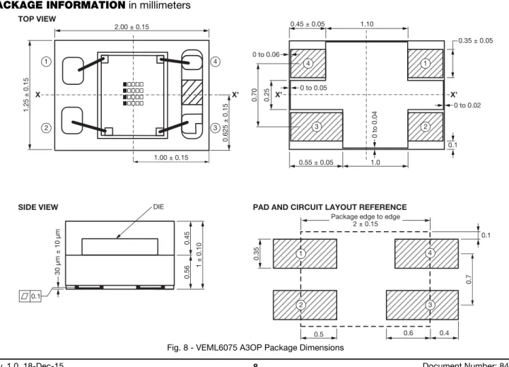
PACKAGE INFORMATION
in millimeters
Fig. 8 - VEML6075 A3OP Package Dimensions
TABLE 6 - 16-BIT DATA FORMAT
VEML6075 16-BIT DATA FORMAT
15 14 13 12 11 10 9 8 7 6 5 4 3 2 1 0
Data byte low Data byte high
Receive byte Read data from VEML6075
Host action
VEML6075 response
S Slave address Wr A Command code A S Slave address Rd A Data byte (LSB) A Data byte (MSB) N P
S = start condition P = stop condition A = acknowledge N = no acknowledge SIDE VIEW 0.56 DIE 30 μm ± 10 μm 0.1 0.45 1 ± 0.10 TOP VIEW X X’ 1 4 2 3 1.00 ± 0.15 0.625 ± 0.15 2.00 ± 0.15 1.25 ± 0.15 X’ X’ 1.10 0.45 ± 0.05 2 1 4 3 0.55 ± 0.05 1.0 0 to 0.04 0 to 0.02 0 to 0.05 0 to 0.06 0.25 0.70 0.1 0.35 ± 0.05 3
Package edge to edge 2 ± 0.15 1 2 3 4 0.35 0.1 0.7 0.5 0.6 0.4
VEML6075
www.vishay.com
Vishay Semiconductors
RECOMMENDED INFRARED REFLOW
Soldering conditions which are based on J-STD-020 C.
Recommend Normal Solder Reflow is 235 °C to 255 °C
Fig. 9 - VEML6075 OPLGA Solder Reflow Profile Chart
RECOMMENDED IRON TIP SOLDERING CONDITION AND WARNING HANDLING
1. Solder the device with the following conditions:
1.1. Soldering temperature: 400 °C (max.)
1.2. Soldering time: 3 s (max.)
2. If the temperature of the method portion rises in addition to the residual stress between the leads, the possibility that an
open or short circuit occurs due to the deformation or destruction of the resin increases.
3. The following methods: VPS and wave soldering, have not been suggested for the component assembly.
4. Cleaning method conditions:
RECOMMENDED STORAGE AND REBAKING CONDITIONS
PARAMETER CONDITIONS MIN. MAX. UNIT
Storage temperature 5 50 °C
Relative humidity - 60 %
Open time - 168 h
Total time From the date code on the aluminized envelope (unopened) - 12 months
Rebaking Tape and reel: 60 °C - 22 h
Tube: 60 °C - 22 h
IR REFLOW PROFILE CONDITION
PARAMETER CONDITIONS TEMPERATURE TIME
Peak temperature 255 °C + 0 °C / - 5 °C (max.: 260 °C) 10 s Preheat temperature range and timing 150 °C to 200 °C 60 s to 180 s Timing within 5 °C to peak temperature - 10 s to 30 s Timing maintained above temperature / time 217 °C 60 s to 150 s Timing from 25 °C to peak temperature - 8 min (max.)
Ramp-up rate 3 °C/s (max.)
-Ramp-down rate 6 °C/s (max.)
-200 150 217 255
Temperature (°C)
Time (s)
t
2t
1 Max. Temperature (260 °C + 5 °C / - 5 °C)/10 s Ramp-Down Rate 6 °C/s (max.) Ramp-Up Rate 3 °C/s (max.) Soldering Zone 60 s to 150 s Ramp-Up Rate 3 °C/s (max.) Pre-Heating Time t2 - t1 = 60 s to 180 sVEML6075
www.vishay.com
Vishay Semiconductors
Rev. 1.0, 18-Dec-15 Document Number: 84304
TAPE PACKAGING INFORMATION in millimeters
Fig. 10 - VEML6070 A3OP Package Carrier Tape Fig. 11 - Taping Direction
Fig. 12 - Reel Dimension
SIDE VIEW
DIMENSION OF CARRIER TAPE
0.28 ± 0.02 TOP VIEW 1.25 ± 0.10 5.50 ± 0.05 1.75 ± 0.10 12.00 + 0.30 - 0.10 4.0 ± 0.1 4.0 ± 0.1 2.0 ± 0.05 Ø 1.5 ± 0.1 Ø 1.0 ± 0.05 R9 max. 2.58 ± 0.10 R9 max. 2.03 ± 0.10 PIN 1