1650 boul. Lionel Boulet, Varennes, QC, Canada J3X 1S2, T: 1 450 929 8154, F: 1 450 929 8102
Progress Report
Contract # W7701-08-5729
Report on Microfabrication Activities
And Characterization of Carbon Nanotube Films and
Coatings for the microbolometer.
Period ending March 31, 2013
Prepared by
Kazem Zandi
Jean Baptiste Kpetsu
And
Andranik Sarkissian
Submitted To
Dr. Philips Laou and Mme Suzanne Paradis
DRDC - Valcartier
March 22, 2013
DRDC-RDDC-2014-C55
CSA:
The scientific or technical validity of this Contract Report is entirely the responsibility
of the Contractor and the contents do not necessarily have the approval or endorsement of
Defence R&D Canada.
CONTENTS
Summary ... 3
1.
Growth and optical characterization of CNT films ... 4
1.1.
New CNT samples
... 4
1.2.
Specular, diffuse, and total reflectance
... 4
1.3.
Transmittance and reflectance before and after CNT growth
... 5
1.4.
Absorption Spectrum of the CNT layers
... 7
2. Ti and YBCO coatings for the dual-band microbolometer ... 9
2.1 Sputter etching and new thick Ti deposition for posts ... 9
a.
Sputter etching of residuals ... 9
b.
New thick Ti films deposition for posts ... 9
2.2 Y-Ba-Cu-O films to be used as thermistors ... 9
2.3 Samples characteristics ... 12
Annex 2: Resistivity/Temperature data for YBCO samples ... 35
3. Microfabrication of Titanium Posts ... 40
3.1 Detection of Ti Posts ... 40
3.2 Continuity of the posts ... 42
3.3 Post continuation fabrication on prototype samples ... 51
Bibliography ... 56
Summary
This report summarizes the progress on growth and characterization of optical characteristics of
CNT carpets, synthesized using MW-PECVD technique. The characterization was mainly carried
out using FTIR spectroscopy. Results of wavelength dependence of transmittance, reflectance
and absorptance of the CNT films are given for various samples synthesized under different
operating conditions of the MW-PECVD reactor.
The report also summarizes the results of efforts that were carried out for optimization of YBCO
film as a sensitive element of microbolometres. The TCR value for the YCBO deposited at high
pressure of 150 mtorr achieved was measured to be -1.8% with an average resistivity of 1400
ȍ
.cm at ro
om temperature.
In a parallel effort microfabrication process for optimization of the complex structures of Ti posts
were carried out in the lab. The SEM characterization technique, as well as EDS analysis,
combined with optical and topographical profilometry have been used to monitor and optimize
the process development. It has been concluded that controlling the thickness of resin deposited
using spin coating is a critical step in achieving optimum post structures.
1. Growth and optical characterization of CNT films
In the last report, reflectance analyses performed on the old aligned carbon nanotube sample
CS089N (CNT/Ni/TiN/Si) revealed a sharp drop in reflectance for the CNT coated sample as
compared to its TiN coated Si substrate. New CNT samples are produced and analyzed hereafter
for their transmittance, reflectance and their absorption characteristics in order to get a complete
and more detailed picture of the near-to-mid IR absorbing properties of our CNTs.
1.1. New
CNT
samples
Three different materials namely titanium nitride (TiN), silicon nitride (Si
3N
4), and silicon
dioxide (SiO
2) were used as sublayers on top of silicon substrates for the CNT growth. The
samples with the electrically conductive TiN sublayer (CS122N) and the electrically insulating
Si
3N
4sublayer (CSiN-15N) led to CNT films that were suitable for the FTIR analyses. For the
SiO
2sublayer, both thermally grown commercial SiO
2film (CSiOc01N) and sputtered SiO
2coating (CSiO-07N) were used and none of them yielded a suitable CNT sample for FTIR
analyses. It’s worth mentioning however that for CSiO
-07N, few CNTs spots were found on the
sample after the CNT growth process but were removed from it by static electricity from a Petri
dish cover. This is indicative of a very poor adhesion of the CNT layer to the SiO
2sublayer.
Therefore, it is very likely that CNTs were grown on our SiO
2sublayer during the growth process
but, due to their poor adhesion to the substrate, were almost completely swept away by gas flow
or any other mean before the samples were removed from the PECVD reactor.
Detailed deposition parameters of all samples are available in the follow-up tables (A) and (B) of
2.3 .
1.2.
Specular, diffuse, and total reflectance
Diffuse and total reflectance measurements were performed on samples CS122N and CSiN-15N
using the integrating sphere accessory "A562-G/Q" with the FTIR spectrophotometer. The setup
has been successfully modified to reduce the strength and the surface of mechanical contact
between the CNT layers and the sphere. Thus, the samples are still of good quality and reliable
subsequent SEM analyses could be performed to help correlate the optical and structural
properties of the CNT films. Specular reflectance is calculated from the diffuse and total
reflectance data and all the three spectra are shown in Figure 1 and Figure 2 respectively for
CS122N and CSiN-15N. For comparison, specular reflectance spectra measured using the
"A510/Q-T" accessory is also shown for each sample. The setup has also been modified for the
latter accessory to avoid mechanical contact between its sample holder and the CNT layers. A
plate from the heating stage unit "A599" has been used to fabricate a new custom sample holder
adapted to the "A510/Q-T" accessory for fragile coatings such as CNTs, hence the added suffix
A599-510 in the legend of the figures.
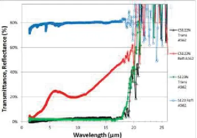
Figure 1 : Total, diffuse, and specular reflectance of a CNT/Ni/TiN/Si sample (CS122N) measured with the integrating sphere A562GQ and its specular reflectance measured with the A510QT accessory
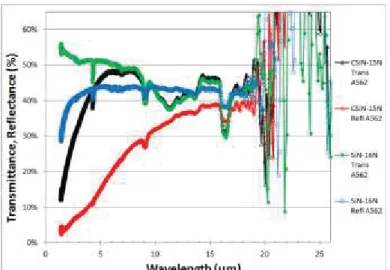
Figure 2 : Total, diffuse, and specular reflectance of a CNT/Ni/Si3N4/Si sample (CSiN-15N) measured with the
integrating sphere A562GQ and its specular reflectance measured with the A510QT accessory
1.3.
Transmittance and reflectance before and after CNT growth
Transmittance and reflectance measurements were performed on CNT samples CS122N and
CSiN-15N as well as on their respective reference substrate S123N (Ni/TiN/Si) and SiN-16N
(Ni/Si
3N
4/Si) using same successful procedures previously established for SiO
2and Si
3N
4samples [1]. Both types of measurement were performed using both the "A510/Q-T" and the
"A562-G/Q" accessories with the same setup modifications described above. Especially for
transmittance measurements with the A562GQ, the very low output signal limitation was
overcome by using the high output power external MIR source mentioned in last report with an
optimized combination of measurement parameters such as the aperture size, the signal gain, and
the scanner velocity. The spectra obtained from the A510QT and A562GQ accessories are
respectively shown in Figure 3 and Figure 4 for the pair (CS122N & S123N) and in Figure 5 and
Figure 6 for the pair (CSiN-15N & SiN-16N).
Figure 3 : Transmittance and specular reflectance of a CNT sample CS122N and its reference substrate S123N (Ni/TiN/Si) measured with the A510QT and its custom substrate holder from A599 plate
Figure 4 : Transmittance and total reflectance of a CNT sample CS122N and its reference substrate S123N (Ni/TiN/Si) measured with the integrating sphere A562GQ
Figure 5 : Transmittance and specular reflectance of a CNT sample CSiN-15N and its reference substrate
Figure 6 : Transmittance and total reflectance of a CNT sample C15N and its reference substrate
SiN-16N (Ni/Si3N4/Si) measured with the integrating sphere A562GQ
1.4.
Absorption Spectrum of the CNT layers
Figure 7 : Absorptance of the CNT layer of samples CSiN-15N and CS122N calculated from transmittance and reflectance data measured with the integrating sphere A562GQ and the A510QT accessory
The absorptance of the CNT layer of samples CS122N and CSiN-15N are calculated from the
corresponding transmittance and reflectance data and shown in Figure 7. These results are quite
different from the near-perfect black reported by Lehman
et al.
for their aligned CNTs of 162
m
of height [2]. Mizuno
et al.
also presented extremely low reflectance measurements of vertically
aligned CNT arrays (less than 1-2%) indicating that it is possible to achieve extremely high
absorptance at wavelengths ranging from the visible wavelengths to 200
ȝ
m
[3].
Although both of our CNT films are still to be characterized by SEM, their height is not expected
to be greater than 12.4
m as previously measured for the sample CS089N (last report) which
growth parameters were similar to CS122N. The quite lower absorptance of our films could
therefore result to some extent from our much shorter CNT layer. The relatively high specular
reflectance and low diffuse reflectance of our samples could be indicative of the CNT layer
density being so low that the almost completely specular reflection from the sublayer is
predominant. The contrary could however also be true since it has been shown that for nanotubes
that are close enough to touch, the coating’s absorptance is about 75% while it rises to 99% when
the CNTs are spaced a few tube diameters apart. [2] It is evidenced that the black body behavior
is not an intrinsic nanotube property but stems from CNT coatings’ unique forest structure, their
sparseness and alignment [3].
The observed differences in absorptance for CS122N and CSiN-15N are thought to arise
essentially from their different sublayer materials since their CNTs were grown simultaneously.
Due to differences in their interfacial energy and interaction parameter, the different sublayer
materials influence differently the nucleation and growth of the Ni catalyst layer leading to
differences in the Ni layer properties (adhesion, particle size and distribution
…)
[4]. This in turn
influences differently the CNT properties such as their diameter, density, growth mode (top or
bottom), adhesion to substrate, and length [5].
2. Ti and YBCO coatings for the dual-band microbolometer
2.1 Sputter etching and new thick Ti deposition for posts
a. Sputter etching of residuals
SEM and EDS analyses performed on few VO
2based bolometer prototypes that are being
fabricated revealed some of the Ti posts were wiped out during lithography processes and were to
be replaced as mentioned in last report. However, observed deposits at the bottom of some vias
were suspected to consist of residuals, silicon nitride, and titanium. Concerns have been raised
about the possible deleterious effects of these deposits and the native oxide on the electrical
conductivity at the junction between the new Ti posts to be deposited and the gold (or chromium
for some samples) layer underneath. To avoid such situation that could prevent any electrical
measurement from being made with the prototypes, we proposed to use the plasma etching
capability of the new Plasmionique SPT330 sputtering system to sputter clean the samples prior
to the new Ti deposition. The sputter etch rates of the various materials were measured and the
appropriate etching parameters determined for each sample based on the evaluation of
thicknesses to be removed without damaging the underneath structure of the devices. Detailed
etching parameters of all samples are available in the follow-up table (C) of 2.3 .
b. New thick Ti films deposition for posts
The need for a high deposition rate and good electrical properties led to the previously optimized
Ti deposition parameters using the "CVC New-Sputter" equipped with a four-inch Ti target
(second to last report). However, since the posts were swept away during lithography processes,
posts with denser Ti were desired for the new films as it could reduce their etching rate and
strengthen their adhesion to the underneath layer. Since the new Plasmionique SPT330 sputtering
system was required for the above-mentioned sputter etching of residuals, the new recipe for
denser Ti deposition was developed using the same system with a new three-inch Ti target. This
was intended to prevent a new native oxide layer to form during the breaking of the vacuum for
sample transfer between the sputter cleaning process and the new Ti deposition. Detailed
deposition parameters for the new thick and denser Ti film are available in the follow-up table
(C) of 2.3 .
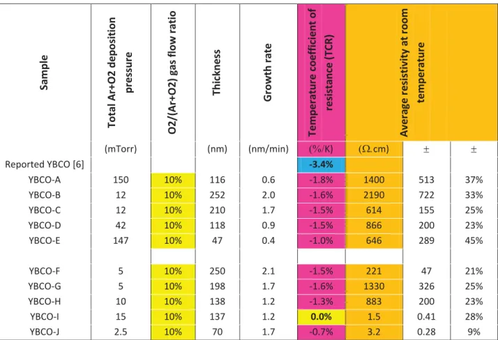
2.2 Y-Ba-Cu-O films to be used as thermistors
New Y-Ba-Cu-O samples (YBCO-F to YBCO-J) were produced using the Plasmionique SPT330
sputter with deposition parameters chosen based on previous optimization results (last and second
to last reports). The O
2gas flow content in the Ar+O
2gas mixture was kept at 10% in the 5-15%
range previously determined and the working pressure was kept in a more conventional
magnetron sputtering pressure range (2.5-15 mTorr ) as compared to up to 150 mTorr previously
for YBCO-A for example. Detailed deposition parameters for the YBCO samples are available in
the follow-up table (C) of 2.3 . Film thickness and hence average growth rate were measured
using the same lithographic and HCl wet etch techniques described in last reports. The resistivity
and temperature measurement curves of the samples are shown in Annex 2. Their temperature
coefficient of resistance (TCR) extracted from those data are available in Table 1 below.
Table 1 : Properties and few deposition parameters of various YBCO samples
Sa
mple
Total A
r+O
2 de
posit
ion
p
re
ssu
re
O2/(Ar+O2
) gas
fl
ow ratio
Thi
ckness
Grow
th rate
Te
mper
atur
e c
o
effic
ient
of
re
si
sta
n
ce
(T
CR)
A
ve
ra
ge
re
si
st
ivit
y a
t
ro
o
m
temperature
(mTorr) (nm) (nm/min) K) :cm) r r Reported YBCO [6] -3.4% YBCO-A 150 10% 116 0.6 -1.8% 1400 513 37% YBCO-B 12 10% 252 2.0 -1.6% 2190 722 33% YBCO-C 12 10% 210 1.7 -1.5% 614 155 25% YBCO-D 42 10% 118 0.9 -1.5% 866 200 23% YBCO-E 147 10% 47 0.4 -1.0% 646 289 45% YBCO-F 5 10% 250 2.1 -1.5% 221 47 21% YBCO-G 5 10% 198 1.7 -1.6% 1330 326 25% YBCO-H 10 10% 138 1.2 -1.3% 883 200 23% YBCO-I 15 10% 137 1.2 0.0% 1.5 0.41 28% YBCO-J 2.5 10% 70 1.7 -0.7% 3.2 0.28 9%Although the coatings of samples such as YBCO-A deposited at a relatively high sputtering
pressure (150 mTorr) are supposed to have a composition much closer to a stoichiometric YBCO
[1], their highest measured average TCR was -1.8%/K which is only ~53% of the reference
reported value of -3.4%/K [6]. Moreover, YBCO-E, which was deposited at quite a similar
pressure (147 mTorr) exhibited a quite different average TCR of -1.0%/K, which is even lower
than the -1.6%/K obtained for YBCO-G that was deposited at 5 mTorr. It thus appears that the
advantage of getting a coating with a composition closer to the stoichiometric YBCO by
increasing the sputtering working pressure do not relate in a simple manner to getting higher
TCR. Reproducibility of the grown YBCO properties might also be a more important issue at
higher pressures (YBCO-A and YBCO-E) than at lower pressure (YBCO-F and YBCO-G) as
shown by the TCR data. Although a high TCR is the more important criteria for the use of our
YBCO films as thermistors, it might be of good advice to use working pressures in the 5 to
15 mTorr
range since our experiments show there’s no guaranty of higher TCR at higher
pressures while deposition challenges increase with such high working pressures. Elsewhere,
porous film structures obtained at higher working pressures would’ve become another is
sue for
the lithography patterning needed for our devices [7]. Pressures lower than 5 mTorr are not
advised since it has been shown that substrate (Si) contaminants could be incorporated inside the
YBCO coatings when the resputtering effect of the sample is too strong [1], which is more likely
to occur at those low working pressures.
For YBCO-I, both negative and positive TCR values in the -1.2%/K to +0.9%/K were obtained
with a strange average value of 0%/K. These results as well as those of YBCO-J are however not
to be considered seriously since the YBCO target has been found to exhibit cracks after those last
two depositions. The fissured target has been replaced with a newer and similar target which is to
be used for upcoming depositions.
2.3
Sa
mples
characteristics
Nomenclature
for
sample
s in the following
table:
Si-0X
:
Si substrate with identification number 0X (
SN0X
for
old samples).
ALN01
:
B
are
Al
2O
3substra
te, number 01.
Ti-0X
:
Si substrate with Ti coating
, numbe
r 0X
.
Bolo9Ti
:
Ti coating
, on
a spec
ia
l substrate (B
olo9 is the name of a devic
e protot
yp
e
used as substrate).
SX01
:
Si substrate with a ther
mall
y
grown ox
ide lay
er
a
t 1000 °C in O
2, number 01.
S012
:
Si substrate with TiN coa
ting
, number 012.
AL07
:
Al
2O
3substra
te with TiN
coating
, numb
er 07.
SiN-0Y
:
Si
3N
4film with identifica
tion number
0Y de
posite
d on an identified substrate.
SiO-0Z
:
SiO
2film wi
th identification number
0Z
d
eposi
ted
on an identified substra
te.
VO2-XX
:
V
O
xfilm with identificat
ion number X
X
de
posite
d on an identified substrate.
YBCO-YY
:
Y-Ba-Cu-O film with ide
ntification number YY d
eposited on a
n identified
substra
te.
SX18N
:
SX18 with Ni coating
.
S100N
:
S100 with Ni coa
ting
.
SN11N
:
SN11 (Si substrate) with Ni coa
ting
, (usua
ll
y for
Ni calibration).
ALN02N
:
A
L
N02 with Ni coatin
g.
CS100N
:
CNT g
ro
w
n on S100N
CALN28N
:
CNT g
rown on AL
N28N
.
Ti-18_pe
:
Plasma etching
o
f sa
mple Ti
-18 using
the Plasmi
onique SPT330 sputter.
A.
Sputte
r deposi
tion w
ith the "CV
C New
-Sputter"
Sample na me Date New-Sputter (NS) Plasmioni que sputter (SPT) Gun Num ber Gun /Ta rget d iam eter ('') Mode: DC o r RF (Contac tor /Gene rator 1 or 2) Targ et Targ et ĺ Substrate Distanc e (cm) Substrate (If in r otatio n) Toggle Ha lf-An gle (±X°) Toggle Velo city Base Pre ssure - Pfeiffer - Cold Catho de (T orr) Base Pressure - Varian - Io n Gau ge (To rr) Real Tem pera ture (°C) Temp erature Setpo int (°C) Sputtering Po wer (W) Reflec ted Powe r (W) Presputtering Time ( min) Sputtering Tim e ( min) DC Bias in RF mode or V olta ge in DC mode (V) Current in DC m ode (A) N2 ad juste d flo w (sc cm ) O2 flo w (sccm ) Ar flo w (sccm ) Depo sition Total Pre ssure - MKS - Baratr on (mTorr) Total Pre sition Depo ssure -
Varia n - CDG (m Torr) Total Pre sition Depo ssure - Varia n - Co nvecTo rr (mTo
rr) ssure Total Pre sition Depo - Pfeiffer - Pira ni (m Torr) Thickness (nm ) De ktak Thickness (nm ) E llipso metry Comme nts TiN 12 /07/ 0 9 NS 1 2 DC -1 TiN 10 Hold e r 10 3 1. 5E -07 3. 6E -07 98 .6 5 10 49 5 0. 20 4 50 0 0 1. 23 3 3. 7 2. 1 4h00 pum pi ng -Tes t b ef or e Ne w C N T s Ni NS 8 4 RF -1 Ni 10 Hold e r 45 3 10 0. 4 4. 3 5 10 - 81 0 0 0 30 0. 75 1. 7 1. 3 1. 5 5 Tes t b ef or e Ne w C N T s S1 18 12 /07/ 1 0 NS 1 2 DC -1 TiN 10 Si 10 3 1. 5E -07 3. 4E -07 50 0 98 .8 30 30 48 6 0. 20 5 50 0 0 1. 2 2. 6 3. 6 2. 1 7 10 0 3h00 pum pi ng -H eating : 25V ,2 5A -Fo r C N T s S1 19 50 0 98 .8 30 30 48 6 0. 20 5 50 0 0 1. 2 2. 6 3. 6 2. 1 7 10 0 3h00 pum pi ng -H eating : 25V ,2 5A -Fo r C N T s S1 20 50 0 98 .8 30 30 48 6 0. 20 5 50 0 0 1. 2 2. 6 3. 6 2. 1 7 10 0 3h00 pum pi ng -H eating : 25V ,2 5A -Fo r C N T s S1 21 50 0 98 .8 30 30 48 6 0. 20 5 50 0 0 1. 2 2. 6 3. 6 2. 1 7 10 0 3h00 pum pi ng -H eating : 25V ,2 5A -Fo r C N Ts Ni 12 /07/ 1 8 NS 8 4 RF -1 Ni 10 Hold e r 45 3 1. 9E -07 4. 4E -07 10 0. 4 5. 5 30 0 - 76 0 0 10 5. 66 12 10 7. 8 3 1h30 pum pi ng ,
Sample na me Date New-Sputter (NS) Plasmioni que sputter (SPT) Gun Num ber Gun /Ta rget d iam eter ('') Mode: DC o r RF (Contac tor /Gene rator 1 or 2) Targ et Targ et ĺ Substrate Dist ance (cm) Substrate (If in r otatio n) Toggle Ha lf-An gle (±X°) Toggle Velo city Base Pre ssure - Pfeiffer - Cold Catho de (T orr) Base Pressure - Varian - Io n Gau ge (To rr) Real Tem pera ture (°C) Temp erature Setpo int (°C) Sputtering Po wer (W) Reflec ted Powe r (W) Presputtering Time ( min) Sputtering Tim e ( min) DC Bias in RF mode or V olta ge in DC mode (V) Current in DC m ode (A) N2 ad juste d flo w (sc cm ) O2 flo w (sccm ) Ar flo w (sccm ) Depo sition Total Pre ssure - MKS - Bara tro n (m
Torr) Total Pre sition Depo ssure -
Varian CDG (mTo
rr) ssure Total Pre sition Depo - Varia n Co nvecTo rr (m
Torr) ssu Total Pre sition Depo re - Pfeiffer - Pira ni (m Torr) Thickness (nm ) De ktak Thickness (nm ) E llipso metry Comme nts 6 Cl ea ni ng 10 0. 4 4. 3 0 30 - 81 0 0 0 30 0. 75 1. 7 1. 3 1. 5 5 Ni 12 /07/ 1 9 NS 8 4 RF -1 Ni 10 Si 45 3 1. 2E -07 2. 8E -07 10 0. 4 4. 7 30 0 - 72 1 0 0 10 5. 76 13 10 7. 8 8 1h30 pum pi ng , T es t w ith subs tr at e 10 0. 4 4. 3 10 2. 5 - 80 7 0 0 29 0. 74 1. 6 1. 3 1. 5 5 2. 7 8 O K Co ating ob se rved Ni 12 /07/ 2 0 NS 8 4 RF -1 Ni 10 Si 45 3 2. 3E -07 5. 4E -07 10 0. 4 3. 8 10 0 - 73 3 0 0 10 5. 76 13 10 7. 8 8 1h10 pum pi ng , T es t w ith subs tr at e 10 0. 4 4. 1 2 2 - 81 0 0 0 30 0. 74 1. 4 1. 3 1. 5 5 2. 2 2 O K Co ating ob se rved Ni 12 /07/ 2 3 NS 8 4 RF -1 Ni 10 Si 45 3 2. 9E -07 6. 7E -07 10 0. 4 4. 1 30 0 - 72 9 0 0 10 5. 58 12 10 7. 8 8 0h40 pum pi ng , Cl ea ni ng S1 18 N 12 /07/ 2 3 NS 8 4 RF -1 Ni 10 S1 18 45 3 2. 8E -07 5. 9E -07 10 0. 4 4. 8 20 0 - 72 7 0 0 10 5. 72 13 10 7. 9 1h15 pum pi ng , Ni for C N T S1 18 N S1 18 10 0. 4 5. 4 5 2. 5 - 81 3 0 0 30 0. 76 1. 4 1. 3 1. 5 6 2. 7 8 SN 18N Si 10 0. 4 5. 4 5 2. 5 - 81 3 0 0 30 0. 76 1. 4 1. 3 1. 5 6 2. 7 8 S1 19 N 12 /07/ 2 3 NS 8 4 RF -1 Ni 10 S1 19 45 3 3. 0E -07 6. 3E -07 10 0. 4 5. 5 15 0 - 72 0 0 10 5. 76 13 10 7. 9 3 1h05 pum pi ng ,
Sample na me Date New-Sputter (NS) Plasmioni que sputter (SPT) Gun Num ber Gun /Ta rget d iam eter ('') Mode: DC o r RF (Contac tor /Gene rator 1 or 2) Targ et Targ et ĺ Substrate Dist ance (cm) Substrate (If in r otatio n) Toggle Ha lf-An gle (±X°) Toggle Velo city Base Pre ssure - Pfeiffer - Cold Catho de (T orr) Base Pressure - Varian - Io n Gau ge (To rr) Real Tem pera ture (°C) Temp erature Setpo int (°C) Sputtering Po wer (W) Reflec ted Powe r (W) Presputtering Time ( min) Sputtering Tim e ( min) DC Bias in RF mode or V olta ge in DC mode (V) Current in DC m ode (A) N2 ad juste d flo w (sc cm ) O2 flo w (sccm ) Ar flo w (sccm ) Depo sition Total Pre ssure - MKS - Bara tro n (m
Torr) Total Pre sition Depo ssure -
Varian CDG (mTo
rr) ssure Total Pre sition Depo - Varia n Co nvecTo rr (m
Torr) ssu Total Pre sition Depo re - Pfeiffer - Pira ni (m Torr) Thickness (nm ) De ktak Thickness (nm ) E llipso metry Comme nts 5 Ni for C N T S1 19 N S1 19 10 0. 4 4. 3 5 3. 7 5 - 81 6 0 0 30 0. 76 1. 5 1. 3 1. 5 7 4. 1 7 SN 19N Si 10 0. 4 4. 3 5 3. 7 5 - 81 6 0 0 30 0. 76 1. 5 1. 3 1. 5 7 4. 1 7 S1 20 N 12 /07/ 2 3 NS 8 4 RF -1 Ni 10 S1 20 45 3 2. 9E -07 6. 0E -07 10 0. 4 5. 5 15 0 - 72 8 0 0 10 5. 79 13 10 7. 9 5 1h10 pum pi ng , Ni for C N T S1 20 N S1 20 10 0. 4 4. 3 5 5 - 81 4 0 0 30 0. 76 1. 4 1. 3 1. 5 8 5. 5 6 SN 20N Si 10 0. 4 4. 3 5 5 - 81 4 0 0 30 0. 76 1. 4 1. 3 1. 5 8 5. 5 6 Si T i-1 12 /07/ 3 1 NS 6 4 RF -1 Ti 10 Si 18 0 3 1. 1E -07 2. 8E -07 10 0. 4 3. 8 2 0 - 12 8 0 15 8. 7 20 15 11 . 9 5h20 pum pi ng + ga s, Shut te r cl os ed 4 20 0. 9 0. 8 2 3. 6 - 16 2 0 4. 1 2. 22 4. 8 3. 6 4. 0 1 24 4 s ubs tr at e pas sag es in fron t of ta rget for ad he sio n la yer Si T iAu -1 2 2 RF -1 Au 13 Si T i-1 20 3 50 1. 8 5 10 - 20 4 0 4. 1 2. 25 5 4 4. 1 16 8 G old la yer for M irror to be us ed for FT IR Ni 12 /10/ 0 9 NS 8 4 RF -1 Ni 10 ho ld er 45 3 5. 9E -07 10 0. 4 5. 4 5 0 - 77 0 0 10 5. 7 13 7. 9 8 1h00 pum pi ng
Sample na me Date New-Sputter (NS) Plasmioni que sputter (SPT) Gun Num ber Gun /Ta rget d iam eter ('') Mode: DC o r RF (Contac tor /Gene rator 1 or 2) Targ et Targ et ĺ Substrate Dist ance (cm) Substrate (If in r otatio n) Toggle Ha lf-An gle (±X°) Toggle Velo city Base Pre ssure - Pfeiffer - Cold Catho de (T orr) Base Pressure - Varian - Io n Gau ge (To rr) Real Tem pera ture (°C) Temp erature Setpo int (°C) Sputtering Po wer (W) Reflec ted Powe r (W) Presputtering Time ( min) Sputtering Tim e ( min) DC Bias in RF mode or V olta ge in DC mode (V) Current in DC m ode (A) N2 ad juste d flo w (sc cm ) O2 flo w (sccm ) Ar flo w (sccm ) Depo sition Total Pre ssure - MKS - Bara tro n (m
Torr) Total Pre sition Depo ssure -
Varian CDG (mTo
rr) ssure Total Pre sition Depo - Varia n Co nvecTo rr (m
Torr) ssu Total Pre sition Depo re - Pfeiffer - Pira ni (m Torr) Thickness (nm ) De ktak Thickness (nm ) E llipso metry Comme nts 1 af te r cl ea ni ng , Tes t 10 0. 4 4. 1 5 0 - 82 1 0 0 30 0. 75 1. 6 1. 5 8 Ni 12 /10/ 0 9 NS 7 2 RF -1 Ni 10 ho ld er 45 3 40 .1 0 N o p lasma - hi gh re fl ec tio n no t r ed uce d TiN 12 /10/ 1 0 NS 1 2 DC -1 TiN 10 Hold e r 10 0 0 Gas A la rm in t he cle an ro om , pu m pi ng al l n igh t TiN 12 /10/ 1 1 NS 1 2 DC -1 TiN 10 Hold e r 10 3 1. 4E -07 4. 4E -07 98 .6 0 25 44 0 0. 22 8 50 0 30 2. 02 4. 7 4 Cl ea ni ng 98 .6 0 15 47 5 0. 21 50 0 0 1. 26 2. 8 2. 1 9 Cl ea ni ng S1 22 12 /10/ 1 1 NS 1 2 DC -1 TiN 10 Si 10 3 1. 7E -07 3. 7E -07 50 0 98 .8 30 30 48 2 0. 20 8 48 . 3 0 0 1. 19 2. 4 3. 8 2. 2 2 10 0 3h00 pum pi ng -H eating : 25V ,2 5A -Fo r C N T s, DC Pow er an d V ol tag e ar e -15 9W an d 21 2V in the s of t, di ffe re nt from M D X-1K
Sample na me Date New-Sputter (NS) Plasmioni que sputter (SPT) Gun Num ber Gun /Ta rget d iam eter ('') Mode: DC o r RF (Contac tor /Gene rator 1 or 2) Targ et Targ et ĺ Substrate Dist ance (cm) Substrate (If in r otatio n) Toggle Ha lf-An gle (±X°) Toggle Velo city Base Pre ssure - Pfeiffer - Cold Catho de (T orr) Base Pressure - Varian - Io n Gau ge (To rr) Real Tem pera ture (°C) Temp erature Setpo int (°C) Sputtering Po wer (W) Reflec ted Powe r (W) Presputtering Time ( min) Sputtering Tim e ( min) DC Bias in RF mode or V olta ge in DC mode (V) Current in DC m ode (A) N2 ad juste d flo w (sc cm ) O2 flo w (sccm ) Ar flo w (sccm ) Depo sition Total Pre ssure - MKS - Bara tro n (m
Torr) Total Pre sition Depo ssure -
Varian CDG (mTo
rr) ssure Total Pre sition Depo - Varia n Co nvecTo rr (m
Torr) ssu Total Pre sition Depo re - Pfeiffer - Pira ni (m Torr) Thickness (nm ) De ktak Thickness (nm ) E llipso metry Comme nts co nt roller va lu es ! Th e ne ga tiv e po w er pr even ts from auto mat ic Wm in co ntr ol o f de po si tio n. C hr on om et e r u se d S1 23 50 0 98 .8 30 30 48 2 0. 20 8 48 . 3 0 0 1. 19 2. 4 3. 8 2. 2 2 10 0 ide m S1 24 50 0 98 .8 30 30 48 2 0. 20 8 48 . 3 0 0 1. 19 2. 4 3. 8 2. 2 2 10 0 ide m S1 25 50 0 98 .8 30 30 48 2 0. 20 8 48 . 3 0 0 1. 19 2. 4 3. 8 2. 2 2 10 0 ide m Si O-07 12 /1 0/ 1 2 NS 8 4 RF -1 Si O2 10 Si 45 3 2. 1E -07 4. 4E -07 40 0 50 0 - 64 2 1 4 2. 35 5. 4 4. 5 4. 2 9 1h10 pum pi ng Si O-07 8 4 40 0 0 11 . 3 - 62 2 1 4 2. 08 4. 7 4 3. 7 8 10 0 T hr ottl ed -Soft w ar e Fw /R ef lec te d RF P ow er (4 76 /39 W ) is v ery di ffe re nt from R FX-60 0 co nt roller va lu es
Sample na me Date New-Sputter (NS) Plasmioni que sputter (SPT) Gun Num ber Gun /Ta rget d iam eter ('') Mode: DC o r RF (Contac tor /Gene rator 1 or 2) Targ et Targ et ĺ Substrate Dist ance (cm) Substrate (If in r otatio n) Toggle Ha lf-An gle (±X°) Toggle Velo city Base Pre ssure - Pfeiffer - Cold Catho de (T orr) Base Pressure - Varian - Io n Gau ge (To rr) Real Tem pera ture (°C) Temp erature Setpo int (°C) Sputtering Po wer (W) Reflec ted Powe r (W) Presputtering Time ( min) Sputtering Tim e ( min) DC Bias in RF mode or V olta ge in DC mode (V) Current in DC m ode (A) N2 ad juste d flo w (sc cm ) O2 flo w (sccm ) Ar flo w (sccm ) Depo sition Total Pre ssure - MKS - Bara tro n (m
Torr) Total Pre sition Depo ssure -
Varian CDG (mTo
rr) ssure Total Pre sition Depo - Varia n Co nvecTo rr (m
Torr) ssu Total Pre sition Depo re - Pfeiffer - Pira ni (m Torr) Thickness (nm ) De ktak Thickness (nm ) E llipso metry Comme nts (4 04 /4 W )! Au to m at ic Wm in co ntr ol o f de po si tio n from soft w ar e va lu es is st ill p os sib le bu t no t reli ab le. C hr on om et e r u se d Si O-08 8 4 40 0 0 11 . 3 - 62 2 1 4 2. 08 4. 7 4 3. 7 8 10 0 ide m Si O-09 8 4 40 0 0 11 . 3 - 62 2 1 4 2. 08 4. 7 4 3. 7 8 10 0 ide m Si O-10 8 4 40 0 0 11 . 3 - 62 2 1 4 2. 08 4. 7 4 3. 7 8 10 0 ide m Si N-1 5 12 /10/ 1 2 NS 8 4 RF -1 Si 3N 4 10 Si 45 3 2. 1E -07 4. 7E -07 20 0 20 0 15 0 - 29 0 1 7 4. 37 10 8. 5 6. 4 5 2h00 pum pi ng + ga s + 0h 35 of 4x 50 de g ste p-he at ing + 20 m in st ab iliz at io n + Pres putte ri n g
Sample na me Date New-Sputter (NS) Plasmioni que sputter (SPT) Gun Num ber Gun /Ta rget d iam eter ('') Mode: DC o r RF (Contac tor /Gene rator 1 or 2) Targ et Targ et ĺ Substrate Dist ance (cm) Substrate (If in r otatio n) Toggle Ha lf-An gle (±X°) Toggle Velo city Base Pre ssure - Pfeiffer - Cold Catho de (T orr) Base Pressure - Varian - Io n Gau ge (To rr) Real Tem pera ture (°C) Temp erature Setpo int (°C) Sputtering Po wer (W) Reflec ted Powe r (W) Presputtering Time ( min) Sputtering Tim e ( min) DC Bias in RF mode or V olta ge in DC mode (V) Current in DC m ode (A) N2 ad juste d flo w (sc cm ) O2 flo w (sccm ) Ar flo w (sccm ) Depo sition Total Pre ssure - MKS - Bara tro n (m
Torr) Total Pre sition Depo ssure -
Varian CDG (mTo
rr) ssure Total Pre sition Depo - Varia n Co nvecTo rr (m
Torr) ssu Total Pre sition Depo re - Pfeiffer - Pira ni (m Torr) Thickness (nm ) De ktak Thickness (nm ) E llipso metry Comme nts Si N-1 5 8 4 20 0 30 0 20 8. 8 4 - 36 5 1 7 3. 1 7. 1 5. 9 5. 2 1 10 0 Dep os it ion af te r 0h 50 of h ea tin g. T hr ottl ed -Soft w ar e Fw /R ef lec te d RF P ow er (4 20 /38 W ) is v ery di ffe re nt from R FX-60 0 co nt roller va lu es (3 01 /2 W )! W att* Mi n-Don e w as 3125 at th e end in soft w ar e ins te ad o f the r eal 2651 for 8, 84 m in ne ed ed for 10 0 nm Si N-1 6 8 4 20 0 30 0 20 8. 8 4 - 36 5 1 7 3. 1 7. 1 5. 9 5. 2 1 10 0 ide m Si N-1 7 8 4 20 0 30 0 20 8. 8 4 - 36 5 1 7 3. 1 7. 1 5. 9 5. 2 1 10 0 ide m
Sample na me Date New-Sputter (NS) Plasmioni que sputter (SPT) Gun Num ber Gun /Ta rget d iam eter ('') Mode: DC o r RF (Contac tor /Gene rator 1 or 2) Targ et Targ et ĺ Substrate Dist ance (cm) Substrate (If in r otatio n) Toggle Ha lf-An gle (±X°) Toggle Velo city Base Pre ssure - Pfeiffer - Cold Catho de (T orr) Base Pressure - Varian - Io n Gau ge (To rr) Real Tem pera ture (°C) Temp erature Setpo int (°C) Sputtering Po wer (W) Reflec ted Powe r (W) Presputtering Time ( min) Sputtering Tim e ( min) DC Bias in RF mode or V olta ge in DC mode (V) Current in DC m ode (A) N2 ad juste d flo w (sc cm ) O2 flo w (sccm ) Ar flo w (sccm ) Depo sition Total Pre ssure - MKS - Bara tro n (m
Torr) Total Pre sition Depo ssure -
Varian CDG (mTo
rr) ssure Total Pre sition Depo - Varia n Co nvecTo rr (m
Torr) ssu Total Pre sition Depo re - Pfeiffer - Pira ni (m Torr) Thickness (nm ) De ktak Thickness (nm ) E llipso metry Comme nts Si N-1 8 8 4 20 0 30 0 20 8. 8 4 - 36 5 1 7 3. 1 7. 1 5. 9 5. 2 1 10 0 ide m Ni 12 /10/ 1 5 NS 8 4 RF -1 Ni 10 ho ld er 45 3 3. 8E -07 9. 2E -07 10 0 0 75 - 76 3 0 0 10 5. 63 13 10 7. 9 5 0h30 pum pi ng f or cl ea ni ng S1 22 N 12 /10/ 1 5 NS 8 4 RF -1 Ni 10 S1 22 45 3 2. 8E -07 6. 1E -07 10 0 25 0 - 72 5 0 0 10 5. 73 13 10 8. 0 2 1h40 pum pi ng , Ni for C N T S1 22 N S1 22 10 0 5 2. 5 - 81 0 0 0 30 0. 76 1. 5 1. 3 1. 5 9 2. 7 8 Si O-07N Si O- 07 10 0 5 2. 5 - 81 0 0 0 30 0. 76 1. 5 1. 3 1. 5 9 2. 7 8 Si N-15N 12 /10/ 1 5 NS 8 4 RF -1 Ni 10 Si N- 15 45 3 3. 1E -07 6. 3E -07 10 0 15 0 - 72 0 0 0 10 5. 79 13 10 8. 0 1 1h15 pum pi ng , Ni for C N T Si N-15N Si N- 15 10 0 5 2. 5 - 81 0 0 0 30 0. 76 1. 7 1. 3 1. 6 2. 7 8 Si Oc 01 N Si Oc 0 1 10 0 5 2. 5 - 81 0 0 0 30 0. 76 1. 7 1. 3 1. 6 2. 7 8 Co mm er cial Si O 2/S i/S iO 2 s ubs tr at e Ni 12 /10/ 1 6 NS 8 4 RF -1 Ni 10 ho ld er 45 3 4. 3E -07 9. 3E -07 10 0 0 45 - 77 8 0 0 10 5. 68 13 10 7. 9 7 0h35 pum pi ng f or cl ea ni ng S1 23 N 12 /10/ 1 6 NS 8 4 RF -1 Ni 10 S1 23 45 3 3. 0E -07 6. 2E -07 10 0 15 0 - 73 0 0 0 10 5. 79 13 10 7. 9 7 1h 05 pum pi ng , Ni for C N T S1 23 N S1 23 10 0 5 2. 5 - 81 0 0 30 0. 76 1. 7 1. 3 1. 5 8 2. 7 8
Sample na me Date New-Sputter (NS) Plasmioni que sputter (SPT) Gun Num ber Gun /Ta rget d iam eter ('') Mode: DC o r RF (Contac tor /Gene rator 1 or 2) Targ et Targ et ĺ Substrate Dist ance (cm) Substrate (If in r otatio n) Toggle Ha lf-An gle (±X°) Toggle Velo city Base Pre ssure - Pfeiffer - Cold Catho de (T orr) Base Pressure - Varian - Io n Gau ge (To rr) Real Tem pera ture (°C) Temp erature Setpo int (°C) Sputtering Po wer (W) Reflec ted Powe r (W) Presputtering Time ( min) Sputtering Tim e ( min) DC Bias in RF mode or V olta ge in DC mode (V) Current in DC m ode (A) N2 ad juste d flo w (sc cm ) O2 flo w (sccm ) Ar flo w (sccm ) Depo sition Total Pre ssure - MKS - Bara tro n (m
Torr) Total Pre sition Depo ssure -
Varian CDG (mTo
rr) ssure Total Pre sition Depo - Varia n Co nvecTo rr (m
Torr) ssu Total Pre sition Depo re - Pfeiffer - Pira ni (m Torr) Thickness (nm ) De ktak Thickness (nm ) E llipso metry Comme nts 7 Si O-08N Si O- 08 10 0 5 2. 5 - 81 7 0 0 30 0. 76 1. 7 1. 3 1. 5 8 2. 7 8 Si N-16N 12 /10/ 1 6 NS 8 4 RF -1 Ni 10 Si N- 16 45 3 2. 9E -07 5. 8E -07 10 0 15 0 - 73 0 0 0 10 5. 81 13 10 7. 9 9 1h15 pum pi ng , Ni for C N T Si N-16N Si N- 16 10 0 5 2. 5 - 82 6 0 0 30 0. 77 1. 8 1. 3 1. 5 9 2. 7 8 Si Oc 02 N Si Oc 0 2 10 0 5 2. 5 - 82 1 0 0 30 0. 76 1. 7 1. 3 1. 6 2. 7 8 S1 24 N 12 /10/ 1 6 NS 4 2 RF -1 Ni 10 S1 24 10 3 3. 7E -07 7. 6E -07 40 15 0 - 67 9 0 28 16 37 28 23 1h00 pum pi ng , Ni for C N T S1 24 N S1 24 40 10 4. 5 - 73 5 0 0 28 . 5 0. 73 1. 5 1. 4 1. 5 1 0! N o co ati ng (e dg e) ob se rved ! To b e co ate d ag ai n Si O-09N Si O- 09 40 10 4. 5 - 73 5 0 0 28 . 5 0. 73 1. 5 1. 4 1. 5 1 0! ide m Si N-17N 12 /10/ 1 6 NS 4 2 RF -1 Ni 10 Si N- 17 10 3 4. 0E -07 8. 1E -07 40 15 0 - 67 6 0 28 . 5 16 .2 2 38 29 23 . 3 0h55 pum pi ng , Ni for C N T Si N-17N Si N- 17 40 5 4. 5 - 74 0 0 0 28 . 2 0. 73 1. 6 1. 3 1. 4 8 7. 1 Co at ing is vi si bl e! Sh ou ld h ave do ne 3m in /4 .3 nm
Sample na me Date New-Sputter (NS) Plasmioni que sputter (SPT) Gun Num ber Gun /Ta rget d iam eter ('') Mode: DC o r RF (Contac tor /Gene rator 1 or 2) Targ et Targ et ĺ Substrate Dist ance (cm) Substrate (If in r otatio n) Toggle Ha lf-An gle (±X°) Toggle Velo city Base Pre ssure - Pfeiffer - Cold Catho de (T orr) Base Pressure - Varian - Io n Gau ge (To rr) Real Tem pera ture (°C) Temp erature Setpo int (°C) Sputtering Po wer (W) Reflec ted Powe r (W) Presputtering Time ( min) Sputtering Tim e ( min) DC Bias in RF mode or V olta ge in DC mode (V) Current in DC m ode (A) N2 ad juste d flo w (sc cm ) O2 flo w (sccm ) Ar flo w (sccm ) Depo sition Total Pre ssure - MKS - Bara tro n (m
Torr) Total Pre sition Depo ssure -
Varian CDG (mTo
rr) ssure Total Pre sition Depo - Varia n Co nvecTo rr (m
Torr) ssu Total Pre sition Depo re - Pfeiffer - Pira ni (m Torr) Thickness (nm ) De ktak Thickness (nm ) E llipso metry Comme nts Si Oc 03 N Si Oc 0 3 40 5 4. 5 - 74 0 0 0 28 . 2 0. 73 1. 6 1. 3 1. 4 8 7. 1 Co at ing is vi si bl e! Sh ou ld h ave do ne 3m in /4 .3 nm
B.
CNT grow
th
w
ith the PECV
D syste
m
Échantill ons Date Press ion de base - Jauge Pfeiffer (To rr) Distance Substr at ĺ Cible o u ĺ Entrée ȝ -onde s (cm) Substrat Porte -substr ats (PECVD) Dépô t - Puiss ance (W) Dépô t - Durée (min) Dépô t - Temp ératu re (°C) Dépô t - Press ion ( mTorr) Dépô t - Ga z H2 (%) Dépô t - Ga z CH4 (% ) Dépô t - Ga z C2H2 (%) Épaisse ur (nm) Pola risat ion DC (V) Autres - comme ntaire s (Chiffre en italiq ue = valeur estimée en fonctio n d e mesures préc édentes ) CS N 18 N 12 /10/ 17 2. 2E -07 27 SN 18N BN 900 20 700 6000 80 20 0 C N T s d ela m ina te s, p oor Ni adh es ion CS N 19N 12 /10/ 17 2. 2E -07 27 SN 19N BN 900 20 700 6000 80 20 0 C N T s d ela m ina te s, p oor Ni adh es ion CS N 20N 12 /10/ 17 2. 2E -07 27 SN 20N BN 900 20 700 6000 80 20 0 C N T s d ela m ina te s, p oor Ni adh es ion CS N 21 12 /10/ 17 2. 2E -07 27 SN2 1 BN 900 20 700 6000 80 20 0 FT IR re fe re nce f or 3 s am pl es abo ve , s am e S i - No Ni , n o C N T CS 118N 12 /10/ 18 1. 4E -07 27 S1 18 N BN 900 20 700 6000 80 20 0 CN T s o n N i/T iN /S i CS 119N 12 /1 0/ 18 1. 4E -07 27 S1 19 N BN 900 20 700 6000 80 20 0 CN T s o n N i/T iN /S i CS 120N 12 /10/ 18 1. 4E -07 27 S1 20 N BN 900 20 700 6000 80 20 0 CN T s o n N i/T iN /S i CS 12 1 12 /10/ 18 1. 4E -07 27 S1 21 BN 900 20 700 6000 80 20 0 FT IR r ef er en ce for 3 s am ples a bove bu t h ea tin g par tial ly ev apo rate s T iN - A voi d h ea tin g for n ext re fe re nc es CS 122N 12 /12/ 14 1. 8E -07 27 S1 22 N BN 900 20 700 6000 80 20 0 C N T s - for FT IR a nd SE M a na ly se s CS iN -1 5N 12 /12/ 14 1. 8E -07 27 SN 19N BN 900 20 700 6000 80 20 0 C N T s - for FT IR a nd SEM a na ly se s CS iO -0 7N 12 /12/ 14 1. 8E -07 27 SN 20N BN 900 20 700 6000 80 20 0 Sm al l C N T s pot s de la m ina te d ue to s ta tic el ec tr ici ty f ro m a P etr i d is h co ve r - Poor Ni ad he sio n? CS iO c0 1N 12 /12/ 14 1. 8E -07 27 SN2 1 BN 900 20 700 6000 80 20 0 No C N T s - Poor Ni a dh es ion ? C N T de la m ina ti on b y ga s f lo w in rea ct or?C.
Sputte
r deposi
tion w
ith the "Plas
m
ioniqu
e SPT3
30" syste
m
Sample na me Date Base Pressure - Varian - Io n Gaug e (Torr) Pres1 Gun Num ber Targ et Material Gun /Ta rget d iam eter ('') Substrate Substrate P ositio n (m m) Targ et ĺ Substrate Dist an ce (cm) Substrate Rot ation Ve locit y(rpm) erature Setpo Temp int Va
lue S V
(°C) erature Pro Temp be Valu e PV from TC1 (°C) Real Sam ple Tem pera ture (°C) Mode-Ma tch : RF-2 , DC-1 Sputtering FW P owe r (W) Reflec ted Powe r (W) Cathod e Voltag e (V) Presputtering Time ( min) Sputtering Tim e ( min) Bias FW P owe r - sam ple (W) Bias Reflec ted Powe r (W) Bias Volt age - s am ple (V) Bias Durati on (m in) N2 flow (sccm) O2 flo w (sccm ) Ar flo w (sccm ) Press ure Control: Ma nua l, Throttle, Fl ow Throttle Va lve (% Close d) Depo sition Total Pre ssure - MKS - Baratr on (
mTorr) Total Pre sition Depo ssure
-
Pfeiffer - CMR (m Torr) Total Pre sition Depo ssure -Varia n - Pres1 (m Torr) Program : M anu al, Au tom atic Thickness (nm ) De ktak Thickness (nm ) E llipso metry Comme nts YB C O-A 12 /09/ 17 7. 9 E- 07 2 Y BCO 3 Si 45 10 10 19 RF -2 20 0 0 76 2 2 18 M 0 OR 15 3 93 M Co at ing an d tar ge t cl ea ni ng -T urb o pu m p w as s to ppe d to al lo w tha t hi gh pr es su re 78 RF -2 20 0 0 54 18 0 2 18 M 0 OR 14 3 77 M 11 6 ide m + Ma te ri al co ate d ins ide ch imne y w al ls p ee ls off: f la kes fa ll d ow n wh en sh utte r op en s YB C O-B 12 /09/ 19 9. 7 E- 07 2 Y BCO 3 Si 45 10 10 19 RF -2 20 0 0 10 8 2 50 0 16 4 2 2 18 F 96 12 9. 4 M 66 RF -2 20 0 1 90 12 5 2 18 F 96 12 4. 8 M 25 2 YB C O-C 12 /09/ 20 5. 4 E- 07 2 Y BCO 3 Si 45 10 10 17 RF -2 20 0 1 89 2 5 45 F 90 12 8. 4 M Sa me pr es su re a s Y BCO -B bu t hig he r ga s f lo w
Sample na me Date Base Pressure - Varian - Io n Gaug e (Torr) Pres1 Gun Num ber Targ et Material Gun /Ta rget d iam eter ('') Substrate Substrate P ositio n (m m) Targ et ĺ Substrate Dist ance (cm) Substrate Rot ation Ve locit y
(rpm) erature Setpo Temp int Va
lue S V
(°C) erature Pro Temp be Valu e PV from TC1 (°C) Real Sam ple Tem pera ture (°C) Mode-Ma tch : RF-2, DC-1 Sputtering FW P owe r (W) Reflec ted Powe r (W) Cathod e Voltag e (V) Presputtering Time ( min) Sputtering Tim e ( min) Bias FW P owe r - sam ple (W) Bias Reflec ted Powe r (W) Bias Volt age - s am ple (V) Bias Durati on (m in) N2 flow (sccm) O2 flo w (sccm ) Ar flo w (sccm ) Press ure Control: Ma nua l, Throttle, Fl ow Throttle Va lve (% Close d) Depo sition Total Pre ssure - MKS - Bara tro n (m
Torr) ssure Total Pre sition Depo -
Pfeiffer - CMR (m Torr) Total Pre sition Depo ssure -Varian - Pre s1 (mT orr) Program : M anu al, Au tom atic Thickness (nm ) De ktak Thickness (nm ) E llipso metry Comme nts (2 .5 X) 69 RF -2 20 0 1 78 12 5 5 45 F 90 12 6 M 21 0 YB C O-D 12 /09/ 20 2. 0 E- 07 2 Y BCO 3 Si 45 10 10 51 RF -2 20 0 1 52 2 5 45 F 97 42 . 5 M 94 RF -2 20 0 1 51 12 5 5 45 F 97 42 5. 9 M 11 8 YB C O-E 12 /09/ 24 2. 9 E- 07 2 Y BCO 3 Si 45 10 10 16 RF -2 20 0 1 48 2 2 18 M 0 OR 14 7 81 M Sa me pa ra me te rs as YB CO -A bu t dif fe re nt pr op er tie s. T urb o pu m p w as s to ppe d to al lo w tha t hi gh pr es su re 83 RF -2 20 0 0 33 12 5 2 18 M 0 OR 14 2 80 M 47 Dek ta k sh ow s a hi gh s urfa ce ro ug hne ss Ti -1 4 12 /11/ 16 5. 9 E- 07 1 Ti 3 Si back 45 10 10 16 RF -1 10 0 0 25 0 3 45 M 92 17 . 6 M 18 RF -2 25 0 1 26 6 2 12 0 10 0 1 22 3 30 45 92 13 . 9 Ma te ri al co ate d ins ide ch imne y w al ls p ee ls