SC339
Ultra Low Output Voltage
Linear FET Controller
POWER MANAGEMENT
Description
Features
The SC339 is an ultra-low output voltage, linear power supply controller designed to simplify power manage-ment for notebook PCs. It is part of Semtech’s Smart
LDOTM family of products. The SC339 has a user
adjustable output that can be set anywhere between 0.5V and 3.3V using two external resistors.
SC339 features include tight output voltage regulation (± % over 0°C to +85°C), enable control, open drain power good signal, under-voltage protection and soft-start. The enable pin allows the part to enter a very low power standby mode. Pulling it high enables the output. The power good pin is an open drain and asserts low when the voltage at the adjust pin is below 88% (typ) of nominal. If the voltage at the adjust pin is below 50% (typ) of nominal, the under-voltage protection circuitry will shut down the output. The SC339 is available in a tiny SOT-23 6-pin surface mount package.
± % Voltage Accuracy Over-Temperature
Low Shutdown Current
Runs Off 5V Supply
Ultra-Fast Transient Response
Enable Control for the Output
Power Good Monitoring and Signaling for the Output
Gate Drive from Input Supply Enables Use ofN-Channel MOSFET
User Selectable Dropout Voltage
Under-Voltage Protection for the Output
SOT-23 6-pin Surface Mount Package
Compatible with Ceramic Capacitors
Low Ripple Output
Internal ms soft-start requires no externalcompo-nents
Fully WEEE and RoHS compliant
Notebook PCs
Desktop Computers
Battery Powered Devices
Portable InstrumentsTypical Application Circuit
Applications
1.05V @ 3A
SC339
IN DRV
ADJ PGD EN
GND
C1
C2
C4 5V IN
1.05V
Enable Power Good1.05V
1.2V +/-5% IN
IRF7311 or similar
Vout= (1+R1/R2)*0.5
Notes:
(1) Optional Components to use with ceramic output capacitors (C2)
C3(1)
R3(1)
R1
SC339
PRELIMINARY
POWER MANAGEMENT
Absolute Maximum Ratings
Parameter Symbol Maximum Units
Input Supply Voltage VIN -0.3 to +6 V
Drive Pin VDRV -0.3 to VIN + 0.3V V
Adjust and Power Good Pin VADJ, VPGD -0.3 to VIN + 0.3V V
Enable Pin VEN -0.3 toVIN + 0.3V V
Thermal Impedance Junction to Ambient θJA 190 °C/W
Thermal Impedance Junction to Case θJC 81 °C/W
Operating Ambient Temperature Range TA -40 to +85 °C
Operating Junction Temperature Range TJ -40 to +125 °C
Storage Temperature Range TSTG -65 to +150 °C
Lead Temperature (Soldering) 10 Sec. TLEAD 300 °C
ESD Rating (Human Body Model) VESD 2 kV
Electrical Characteristics
Unless specified: TA = 25°C, VIN = VEN = 5V ± 5%, VPWR() = .5V ± 5%, 0A ≤ IOUT≤ 3A. Values in bold apply over full operating ambient temperature range. Exceeding the specifications below may result in permanent damage to the device or device malfunction. Operation outside of the parameters specified in the
Electrical Characteristics section is not implied. Exposure to absolute maximum rated conditions for extended periods of time may affect device reliability.
Parameter Symbol Conditions Min Typ Max Units
Supply Voltage VIN 4.5 5 5.5 V
Quiescent Current IQ VIN = 5V 130 200 µA
Standby Current IQ(OFF) EN low 0.1 1.0 µA
Input Under-Voltage Lockout
Start Threshold VUVLO VIN rising 4.20 V
Hysteresis VHYST VIN falling 0.10 V
EN
Enable Input Threshold VIH Output on 2.8 V
VIL Output off 1.8
SC339
POWER MANAGEMENT
Parameter Symbol Conditions Min Typ Max Units
ADJ
Adjust Input Bias Current IADJ VADJ = 0.5V -100 0 +100 nA
Reference Voltage VADJ 0°C ≤ TA ≤ +85°C -1% 0.500 1% V
DRV
Output Current IDRV Sourcing 5 20 mA
Sinking 5 20 mA
Output Voltage VDRV Full On, IDRV = 0mA, VIN = 5V 4.70 4.85 V
Output Under-Voltage Protection
Trip Threshold(2) V
TH(UV) Measured at ADJ pin 40 50 60 %VADJ
PGD
Power Good Threshold(3) V
TH(PGD) Measured at ADJ pin -15 -12 -8 %VADJ
Output Logic Low Voltage VPGD VADJ = 0.4V, IPGD = -1mA 0.4 V
Power Good
Leakage Current IPGD VADJ = 0.5V, 0V≤ VPGD ≤ VIN -1 0 +1 µA
Soft-Start
Output Rise Time 10% VOUT
to 90% VOUT, VOUT = 1.05V tr
From EN rising to
99% of VOUT 500 1000 2000 µs
Electrical Characteristics
Notes:
) VPWR = input voltage to pass device drain (or source depending upon orientation of FET). 2) If VTH(UV) is exceeded for longer than ms (nom.) the protection circuitry will shut down the output. 3) During start-up only, VTH(PGD) is -6% (typical), then switches to -2% (typical).
SC339
PRELIMINARY
POWER MANAGEMENT
Pin Descriptions
Notes:
) Only available in tape and reel packaging. A reel contains 3000 devices.
2) VIN = 5V
3) VADJ is ± 1% over 0°C ≤ TA ≤ +85°C.
) Lead-free product. This product is fully WEEE and RoHS compliant.
Pin Configuration
Ordering Information
Part Number Package
SC339SKTRT SOT-23 6 Pin
SC339EVB Evaluation Board
Pin Pin Name Pin Function
1 IN 5V supply
2 GND Ground
3 EN Active high enable control - connect to IN if not being used - do not allow to float
4 PGD Power good signal output for VOUT
5 ADJ Regulator sense input - used for sensing the output voltage for power good and under-voltage and to set the output voltage
6 DRV Output of regulator - drives the gate of an N-channel MOSFET to maintain VOUT
set by R1 and R2
Marking Information
1
4 5 6
3 2
DRV IN
EN PGD
GND ADJ
Top View
(SOT-23 6L)
Marking for SOT23, 6 lead package: yyww = Datecode (Example: E652)
SC339
POWER MANAGEMENT
Block Diagram
Shutdown Control
Under Voltage Control
+
-+
+
-Vref
0.5 VBG
0.88 VBG
(0.95 VBG At start-up)
Power Good Comparator
Vref ( 0.5V) EN
DRV
PGD
IN
ADJ 0.5V
Bandgap Reference
Undervoltage Comparator
Error Amplifier
SC339
PRELIMINARY
POWER MANAGEMENT
Applications Information
Theory Of OperationThe SC339 linear FET controller provides a simple way to drive an N-channel MOSFET to produce tightly regulated output voltages from an available, higher, supply voltage. It takes its power from the 5V system supply, drawing 30µA (typ) while operating.
It contains an internal bandgap reference which is compared to the output voltage via a resistor divider. The resistor divider is external and user selectable. The drive pin (DRV) can pull up to a guaranteed minimum of .7V. Thus, the device can be used to regulate a large range of output voltages by careful selection of the external MOSFETs (see Component Selection on this page).
The SC339 includes an active high enable control (EN). If this pin is pulled low, the drive pin is pulled low, turning off the N-channel MOSFET. If the pin is pulled up to 2.8V
≤ VEN ≤ VIN, the drive pin is enabled. This pin should not
be allowed to float.
The SC339 has a power good output (PGD) which is an open drain output that pulls low if the related output is below the power good threshold (-2% of the programmed output voltage typical). The power good circuitry is active if the device is enabled, regardless of the state of the over-current latch.
An over-current protection circuit monitors the output voltage. If the output voltage drops below 50% (typical) of nominal, as would occur during an over-current or short condition, the device will pull the drive pin low and latch off. Toggle the power supply or enable pin to reset the latch condition. Drive Output
The drive output is source and sink capable. The drivers both source and sink 20mA of current typically at 5V IN. Soft-Start and Power Good Timing
At start-up, the internal reference is switched from its normal 0.5VDC to a ms (typical) linear ramp. The output voltage tracks the ramp until 0.5V is reached. The PWRGD signal is held low until the output has been in regulation approximately 500µsec to allow the output voltage to
stabilize. The power-up is very smooth and monotonic. OCP and Power Supply Sequencing
The SC339 has output under-voltage protection that
looks at the output to see if it is: a) less than 50%
(typi-cal) of its nominal value and, b) VDRV for that output is
within 350mV (typical) of maximum. If both of these criteria are met, there is a ms (typical) delay and then the output is shut down. This provides inherent immunity to UV shutdown at start-up (which may occur while the output capacitors are being charged).
At start-up, it is necessary to ensure the power supplies and enable are sequenced correctly to avoid erroneous latch-off. For UV latch-off not to oc-cur at start-up due to sequencing issues, the volt-age supplied to the MOSFET drain should be greater than the output under-voltage threshold when that output is enabled. This assumes that the drop through the pass MOSFET is negligible. If not, then this drop needs to
be taken into account also since:
VOUT = VDRAIN - (IOUT x RDS(ON))
If the supply to the SC339 IN pin comes up before the supply to the MOSFET drain, then that output should be enabled after the supply to the MOSFET drain is applied - the power good signal for this rail would be ideal. If the power supply to the MOSFET drain comes up before the power supply to the SC339 IN pin, then the output can either be enabled with the supply to the IN pin or afterwards.
Please note the following example:
SC339 powered from 5V, the MOSFET (VDRAIN) powered from
.8V, set for .5VOUT. Worst-case: under-voltage threshold is
60% (over temperature) of .5V, or 0.9V. The typical enable threshold is ~2.V, see Figure on Page 7.
Component Selection
Output Capacitors: low ESR capacitors such as Sanyo POSCAPs or Panasonic SP-caps are recommended for bulk capacitance, with ceramic bypass capacitors for decoupling high frequency transients. Ceramic output capacitors may be used; however, use of ceramic output capacitors requires compensation on the DRV output.
SC339
POWER MANAGEMENT
Applications Information (Cont.)
Note: RDS(ON) must be met at all temperatures and at the
mini-mum VGS condition.
Setting The Output Voltage: the adjust pin connects
directly to the inverting input of the error amplifier, and
the output voltage is set using external resistors (please refer to the Typical Application Circuit on Page ).
Using output as an example, the output voltage can be
calculated as follows:
R
VOUT = 0.5 • ( + —— )
R2
The input bias current for the adjust pin is so low that it can be safely ignored. To avoid picking up noise, it is recommended that the total resistance of the feedback
chain be less than 00kΩ. With ceramic capacitors, a
recommended divider current of >00µA is recommended to keep the FET conducting during light load conditions to improve transient response.
SC339 Supply Comes Up Before MOSFET Drain Supply
MOSFET Drain Supply Comes Up Before SC339 Supply 2.8V
2.7V
Power Supply Sequencing
Input Capacitors: placement of low ESR capacitors such
as Sanyo POSCAPs or Panasonic SP-caps at the input to
the MOSFET (VDRAIN) will help to hold up the power supply
during fast load changes, thus improving overall transient
response. If VDRAIN is located at the bulk capacitors for
the upstream voltage regulator, additional capacitance may not be required. In this case a 0.µF ceramic
capacitor will suffice. The 5V bias supply to the SC339
should be bypassed with a 0.µF ceramic capacitor.
MOSFETs: very low or low threshold N-channel
MOSFETs are required. Select FETs rated for VGS
of 2.7V or lower. For the device to work under all
operating conditions, a maximum RDS(ON) must be met to
ensure that the output will never go into dropout:
VIN(MIN) ― VOUT(MAX) RDSON(MAX) = ——————— Ω
SC339
PRELIMINARY
POWER MANAGEMENT
Table lists recommended resistor values for some stan-dard output voltages. All resistors are %, /0W.
The maximum output voltage that can be obtained from each output is determined by the input supply
voltage and the RDS(ON) and gate threshold voltage of the
external MOSFET. Assuming that the MOSFET gate threshold voltage is sufficiently low for the output
voltage chosen and the worst-case drive voltage, VOUT(MAX)
is given by:
VOUT (MAX) = VDRAIN(MIN) ― IOUT(MAX) • RDSON(MAX)
Recommended Resistor Values For SC339 Design Example
Goal: 1.05V±5% @ up to 2.5A from 1.2V±5% and 5V±5%
Solution 1: No Passive Droop
Total window for DC error, ripple and transient is ±52.5mV.
Since this device is linear and assuming that it has been designed to not ever enter dropout, there is negligible ripple on the output.
The DC error for this output is the sum of:
VADJ accuracy = ±% = ±0.5mV
Feedback chain tolerance = ±% = ±0.5mV Load regulation = ±0.25% = ±2.6mV
Resistors per Table should be .0kΩ (top) and 0.0kΩ
(bottom).
VOUT (V) R1 or R3 (kΩ) R2 or R4 (kΩ)
1.05 11.0 10.0
1.2 14.0 10.0
1.5 20.0 10.0
2.5 45.3 11.3
3.3 63.4 11.3
Applications Information (Cont.)
Total DC error = ±2.25% = 23.6mV
This leaves ±2.75% = 28.875mV for the load transient ESR
spike, therefore:
28.875mV
RESR(MAX) = —————— = .55mΩ
2.5A
Bulk capacitance required is given by:
dl • τ
CBULK(MIN) =——— =µF dV
Where dI is the maximum load current step, t is the maximum regulator response time and dV is the allowable voltage droop. Therefore with dI = 2.5A,
t = 1µs, and dV = 28.875mV:
2.5 • • 0¯ 6
CBULK(MIN) = ———————— = 87µF
28.875 • 0¯3
So if we use % VOUT set resistors we would select
00µF, 2mΩ POSCAP for output capacitance (which
assumes that local ceramic bypass capacitors will
absorb the balance of the (2 - .55)mΩ ESR
requirement - otherwise 0mΩ capacitors should be
used).
If we use 0.% set resistors, then the total DC error becomes ±.35% = ±5.75mV, leaving ±3.65% = 38.33mV
for the ESR spike. In this case:
38.33mV
RESR(MAX) = ————= 5.33mΩ and, 2.5A
= 2.5 • • 0¯
6
CBULK(MIN) ——————— = 65µF
38.33 • 0¯3
So for 0.% resistors we could use x 00µF, 5mΩ
SC339
POWER MANAGEMENT
This is a very severe example, since the output voltage is so low, therefore the allowable window is very small. See Solution 2 for an alternate circuit. For higher output voltages the components required will be less stringent.
The input capacitance needs to be large enough to stop the input supply from collapsing below -5% (i.e., the design minimum) during output load steps. If the input to the pass MOSFET is not local to the supply bulk capacitance then additional bulk capacitance may be required.
MOSFET selection: since the input voltage to the SC339 is 5V±5%, the minimum available gate drive is:
VGS = (4.4 ― 1.1025)= 3.3V
So a MOSFET rated for VGS = 2.7V will be required, with an
RDS(ON)(MAX) (over-temperature) given by:
(VIN(MIN) ― VOUT ) (1.14 ― 1.05)
RDSON(MAX) =—————— = ——————= 36mΩ
IOUT(MAX) 2.5
MOSFET SELECTION SO-8 Footprint
Vgs Rds-on Imax
FDS6682 .7V 9mΩ A
IRF756 .5V 6.5mΩ 6A
206 Footprint
Vgs Rds-on Imax
Si506DC 0.6V 20mΩ 9.5A
NTHS50 0.6V 25mΩ 7.2A
SOT-23 Footprint
Vgs Rds-on Imax
IRLMS2002 V 30mΩ 5.2A
FDN337N (when Input
is > .2V for .05V output)
0.7V 65mΩ 2.2A
Solution 2: Using Passive Droop
Passive droop allows us to use almost the full output tolerance window for transients, therefore making the output capacitor selection simpler and less expensive. The trade-offs are the cost of the droop resistor versus the reduction in output capacitor cost, and the reduction in headroom which impacts MOSFET selection. The top of the feedback chain connects to the
input side of RDROOP, and the output is set for .075V. Thus
at no load, VOUT will be .075V (or .05V + 2.%) and at IOUT
= 2.5A, VOUT will be .025V (or .05V - 2.%).
If % set resistors are used, the total DC error will be ±2.25% = 2mV. Thus, at no load, the minimum output
voltage will be given by:
VOUT(MIN_NO_LOAD)= 1.075 ― 0.024 = .05V
This leaves 53.5mV for transient response, giving:
53.5mV = 2.mΩ and,
RESR(MAX)= ————
2.5A
2.5 • • 0¯6 = 7µF
CBULK(MIN)= ———————
53.5 •0¯3
Instead of 2 x 00µF, 2mΩ capacitors, we can use x
7µF, 5mΩ capacitor.
Applications Information (Cont.)
1.075V 1.2V +/-5% IN
1.05V @ 2.5A
C1 0.1uF
R1 11.0k C3
100uF, 25mOhm POSCAP 4
5 6 R2 10.0k RDROOP 20mOhm Q1 IN GND EN DRV ADJ PGD 1 3 2 U1 SC339
SC339
PRELIMINARY
POWER MANAGEMENT
Applications Information (Cont.)
Using Ceramic Capacitors
SC339 is capable of operation using an all-ceramic so-lution, needing only an external R-C compensation. The Typical Application schematic (R3, C3) from page is
re-produced here:
1.05V @ 3A
SC339 IN DRV ADJ PGD EN GND C1 C2 C4 5V IN 1.05V
Enable Power Good1.05V
1.2 V +/-5 % IN
IRF7311 or similar
Vout = (1+R1/R2)*0.5
Notes :
(1 ) Optional Components to use with ceramic output capacitors
C 3 (1)
R 3 (1)
R1
R2
( )C2
Typical Applications Circuit
100 1K 10K 100K 1MEG 10MEG
-40 -20 20 40 60 0,0 Gain (dB) FREQ (Hz) Low frequency pole
generated internally
Pin Low frequency zero generated internally Zin
Rout / Cout pole, moves with the load current Prout
High frequency pole generated by ESR and Output Capacitor
Ceramic Capacitor operation with very low ESR for the output capacitor . We get a three pole 1 zero system as shown above and is unstable without external compensation
Pcout -60 -90 -180 90 180 270 -270 PHASE PHASE (deg)
Typical Frequency Response without Compensation and Ceramic Output Capacitors:
SC339 Frequency Response with
Ceramic Output Capacitors and no Compensation
From this response we see that the system is not stable as it has a phase margin of approximately 0 degrees. For stable operation we introduce a low frequency pole and a zero. The low frequency pole is used to roll off the gain quicker and the zero is used to increase the band-width of the system.
The Pole-Zero location:
100 1K 10K 100K 1MEG 10MEG
-40 -20 20 40 60 0,0 Gain (dB) FREQ (Hz) Pin + Pcomp
Zin + Zcomp
Prout
Ceramic Capacitor Operation with Compensation on DRV pin
Pcout -60 -90 -180 90 180 270 -270 PHASE PHASE (deg)
SC339 Frequency Response with
Ceramic Output Capacitors and R-C Compensation
From the above figure we can see that the overall re -sponse of the system is stable with a decent phase margin
It is important to select the external compensation zero to be between kHz and 5 kHz for optimum bandwidth and phase margin. In this example we have selected zero at approximately 3 kHz.
The compensation values are calculated by the following
empirical equation:
We chose a low R3 compensation value to roll off gain.
R3 = 100 Ω.
SC339
POWER MANAGEMENT
Applications Information (Cont.)
Now,
We choose C3 = 70nF as the standard value. Soft-Start Behavior
At start-up, VOUT first ramps linearly from ground at the rate of
~0.5V/ms (+/- 25%) for about 800us. The linear ramping is followed by a phase of smooth settling for about 700us at the end of which the output has fully settled (to better than %). The total start-up time of about .5ms is kept within ms
- 2ms window, and this is regardless of the loading and
of the external components connected to the device.
SC339 Start-Up Response
C3 = ½•�• R3 • 3kHz = 530nF
Layout Guidelines
The advantages of using the SC339 to drive external
MOSFETs are:
a) that the bandgap reference and control circuitry are in a die that does not contain high power dissipating devices and,
b) that the device itself does not need to be located right next to the power devices. Thus very accurate output voltages can be obtained since changes due to heating effects will be minimal.
The 0.µF bypass capacitor should be located close to the supply (IN) and GND pins, and connected directly to the ground plane.
The feedback resistors should be located at the device, with the sense line from the output routed from the load (or top end of the droop resistor if passive droop is being used) directly to the feedback chain. If passive droop is being used, the droop resistor should be located next to the load to avoid adding additional unplanned droop. Sense and drive lines should be routed away from noisy traces or components.
For very low input to output voltage differentials, the input to output/load path should be as wide and short as possible. Where greater headroom is available, wide
traces may suffice.
Power dissipation within the device is practically negligible, thus requiring no special consideration dur-ing layout. The MOSFET pass devices should be laid out according to the manufacturer’s guidelines for the power being dissipated within them.
SC339
PRELIMINARY
POWER MANAGEMENT
Performance Characteristics
Supply Current vs. Supply Voltage
VCC = 4.5V to 5.5V, IOUT = 2.5A, VIN = 1.5V, VEN = 5V
125.0E-6 130.0E-6 135.0E-6 140.0E-6 145.0E-6 150.0E-6 155.0E-6 160.0E-6
4.500 4.600 4.700 4.800 4.900 5.000 5.100 5.200 5.300 5.400 5.500
VCC (V)
ICC
(A
)
Supply Current
Figure 1: Supply Current v/s Supply Voltage
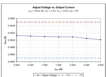
Adjust Voltage vs. Output Current
IOUT = 0A to 3A, VIN = 1.5V, VCC = 5.0V, VEN = 5V
0.4940 0.4960 0.4980 0.5000 0.5020 0.5040 0.5060
0.000 0.500 1.000 1.500 2.000 2.500 3.000
IOUT (A)
VAD
J
(V
)
Adjust Voltage +1% -1%
Figure 2: Adjust Voltage v/s Output Current (1% accurate)
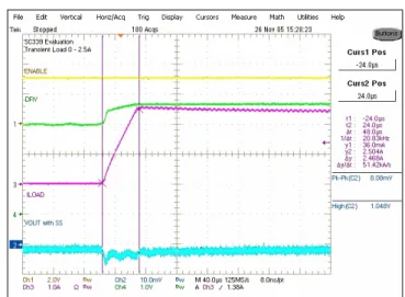
Figure 3: Soft Start waveform shows the PWRGD delay
Figure 4: Input UVLO Test (Rising)
SC339
POWER MANAGEMENT
Performance Characteristics
Figure 7: Enable threshold detect (Falling) Figure 8: Transient load rising edge
SC339
PRELIMINARY
POWER MANAGEMENT
Outline Drawing - SOT-23 6
.110 BSC .037 BSC DETAIL aaa C SEATING ccc C 2X N/2 TIPS
2X E/2 6 SEE DETAIL A1 A A2 bxN A .008 1 2 N E
.060 .114.063 .118 .010 -6 A 0.20 1.60 3.00 2.80 BSC 0.95 BSC .069 1.50 2.90 .020 0.25 1.75 0.50 -EI L (L1) c 01 0.25 PLANEGAGE H 2.80 .110
bbb C A-B D
0° .008 -.004 .012 .003 (.024).018 -.035 .000 .035 -.045 0.10 0.20 10° 0° - 10°
1.15 (0.60)0.45 .024 .009 0.30 0.08 .057 .051 .006 0.00 .90 0.90 0.22 0.60 -0.15 1.45 1.30 -1.90 BSC .075 BSC A e1 D e B C H NOM INCHESDIMENSIONS L1 aaa bbb ccc 01N DIM c e e1 L E1 E D A1 A2 b A MIN MILLIMETERS MAX MIN NOM MAX
PLANE
D
DATUMS AND TO BE DETERMINED AT DATUM PLANE CONTROLLING DIMENSIONS ARE IN MILLIMETERS (ANGLES IN DEGREES). DIMENSIONS "E1" AND "D" DO NOT INCLUDE MOLD FLASH, PROTRUSIONS 3.
OR GATE BURRS. NOTES:
1.
2. -A- -B-
SC339
POWER MANAGEMENT
THIS LAND PATTERN IS FOR REFERENCE PURPOSES ONLY. CONSULT YOUR MANUFACTURING GROUP TO ENSURE YOUR COMPANY'S MANUFACTURING GUIDELINES ARE MET.
NOTES: 1.
DIMENSIONS
INCHES
Y Z
DIM
G P X C
MILLIMETERS
P
(C) Z
Y G
.043 .141 .055 (.098)
.037 .024
1.40 (2.50)
0.95 0.60 1.10 3.60
X
DIMENSIONS
INCHES
Y Z
DIM
G P X C