DEVELOPMENT OF NANOFLUIDIC DEVICES FOR SINGLE-MOLECULE DNA DIAGNOSTICS
Franklin Ifeanyichukwu Uba
A dissertation submitted to the faculty at the University of North Carolina at Chapel Hill in partial fulfillment of the requirements for the degree of Doctor of Philosophy in the department
of Chemistry in the school of Arts and Sciences.
Chapel Hill 2014
© 2014
ABSTRACT
Franklin Ifeanyichukwu Uba: Development of Nanofluidic Devices for Single-Molecule DNA Diagnostics
(Under the direction of Steven Soper)
Fluidic devices that possess structures less than 150 nm in one or two dimensions are generating great interest due to the unique properties afforded by this size domain not accessible at the microscale. As molecules travel through nanochannels, they undergo hydrophobic and van der Waals interactions with the channel walls at a degree that depends on the size of the channel, the surface chemistry of the wall and the debye length (governed by the ionic strength of the electrolyte solution). In this work, we report the fabrication of nanometer sized structures (nanoslits, nanochannels and nanoelectrodes) in thermoplastic and fused silica substrates for the analysis of dsNA.
In the case of thermoplastics, mixed-scale micro- and nanofluidic networks were
fabricated using a simple, high resolution, single-step thermal embossing process and the fluidic structures were enclosed via low temperature fusion bonding to a cover plate. Nanochannels were chemically modified and the associated electrokinetic parameters – surface charge density, zeta potential and electroosmotic flow – were evaluated. In the fused silica substrate, we
To God be the glory great things He has done
ACKNOWLEDGEMENTS
I would like to express my sincere gratitude to my advisor, Professor Steven Allan Soper for his unwavering support and encouragement throughout this research work. He is the best mentor any student could ask for and his unwavering assistance has made this work a success. I am also grateful to the members of my dissertation committee, Professor James Jorgenson, Professor Royce Murray, Professor Valarie Ashby, Prof. Anne Taylor and Prof. Matthew Lockett for their time, support and insightful contributions towards the realization of my degree.
I would also like to thank Prof. Yoon-kyoung Cho and Prof. Heungjoo Shin for the invitation to embark some aspects of this research work in conjunction with the World Class University (WCU) program at Ulsan National Institute of Science and Technology. I also thank Mr. Dong-kyu Park of UNIST, Dr. Amar Kumbhar, Dr. Carrie Donley of CHANL and Dr Jennifer Marks of the Olympus research center for their assistance.
I also appreciate past and current members of the Soper research group, most importantly Dr. Rattikkan Chantiwas, Dr. Jiahao Wu, Dr. Nyote Calixte, Dr. Matt Hupert, Dr. Maggie Witek and Dr. Hong Wang and colleagues (Kumuditha Ratnayake, Bo Hu, Matt Jackson and Colleen O’Neil) for their helpful contributions. You guys are awesome!!
TABLE OF CONTENTS
LIST OF TABLES……….………xii
LIST OF FIGURES……….………...………..xiii
LIST OF SCHEMES………..…………..…..xxii
LIST OF ABBREVIATIONS... xxiii
CHAPTER 1: NANOFLUIDICS FOR BIOPOLYMER ANALYSIS ... 1
Introduction ...1
1.1 Parameters in Nanofluidics ...4
1.1.1 Electric Double Layer (EDL) ...4
1.1.2Zeta Potential (or Electrokinetic Potential) ...6
1.1.3Electrical Conductivity ...7
1.1.4Electroosmotic Flow (EOF) ...9
1.2 Nanoscale Phenomena ... 11
1.3 DNA Molecule as a Model Polymer in Nanofluidics ... 13
1.4 DNA Confinement in Nanochannels ... 15
1.5 Effects of Ionic Environment on DNA Molecules ... 17
1.6 Nanochannel fabrication ... 18
1.6.1 Nanochannel fabrication in inorganic substrates ... 19
1.6.2Nanochannel Fabrication in Organic Substrates ... 20
1.6.2.1Elastomeric Nanofluidic Devices ... 20
1.7 Applications of Nanochannels ... 23
1.7.1Nanochannels for the analysis of Biopolymers ... 23
1.7.1.1Optical Detection ... 24
1.7.1.2Electrical Detection ... 30
1.7.2Other applications of nanochannels ... 34
1.8 Overall dissertation outline ... 35
REFERENCES…… ... 38
CHAPTER 2: SURFACE CHARGE, ELECTROOSMOTIC FLOW AND DNA EXTENSION IN CHEMICALLY MODIFIED THERMOPLASTIC NANOSLITS AND NANOCHANNELS1... 49
Introduction ... 49
2.1 Experimental Methods ... 52
2.1.1Materials and Reagents ... 52
2.1.2Fabrication of Nanofluidic Devices ... 53
2.1.3Surface Modification ... 54
2.1.4Water Contact Angle and Surface Energy Determinations ... 55
2.1.5Atomic Force Microscopy (AFM) Measurements ... 55
2.1.6Scanning Electron Micrographs (SEM) Measurements ... 56
2.1.7Surface Charge Measurements ... 56
2.1.8Electroosmotic Flow (EOF) Measurements ... 57
2.1.9Transport Dynamics of λ-DNA through Thermoplastic Nanochannels .... 57
2.2 Results and Discussion ... 58
2.2.1Device Fabrication ... 58
2.2.3Surface Energy (SE) of u-PMMA and O2-PMMA surfaces ... 63
2.2.4Surface Modification of Poly (methyl methacrylate) (PMMA) ... 64
2.2.4.1X-ray Photoelectron Spectroscopy (XPS) Analysis of Plasma treated PMMA Substrates and Nanoslits ... 65
2.2.4.2Fourier Transform Infra-red (FTIR) spectra ... 68
2.2.5Surface Topographical Studies of Modified PMMA Nanoslits ... 69
2.2.6Electrical Model of Nanofluidic Device for Conductance Measurement.. 71
2.2.7Surface Charge and pH Effects ... 73
2.2.8Electroosmotic Flow (EOF) Measurements ... 79
2.2.9Transport Dynamics of λ-DNA through Thermoplastic Nanochannels. ... 82
2.3 Conclusion ... 87
REFERENCES… ... 89
CHAPTER 3: HIGH PROCESS YIELDS OF THERMOPLASTIC NANOFLUIDIC DEVICES USING A HYBRID THERMAL ASSEMBLY TECHNIQUE2 ... 96
Introduction ... 96
3.1 Experimental Methods ... 100
3.1.1Materials and Reagents ... 100
3.1.2Device Fabrication ... 100
3.1.3Water Contact Angle Measurements ... 102
3.1.4Bond Strength Measurements ... 103
3.1.5Surface Charge Measurements ... 103
3.1.6Atomic Force Microscopy (AFM) and Scanning Electron Micrographs (SEMs) ... 105
3.2 Results and Discussions ... 106
3.2.1Water Contact Angle Measurements ... 106
3.2.2Bond Strength Determinations ... 111
3.2.3Surface Charge Measurements ... 114
3.2.4Operational Characteristics of Nanofluidic Devices ... 117
3.3 Conclusion ... 121
REFERENCES……. ... 123
CHAPTER 4: DEVELOPMENT OF NANOFLUIDIC DEVICES FOR THE ELECTRICAL DETECTION OF DNA ... 127
Introduction ... 127
4.1 Experimental Methods ... 129
4.1.1Device Fabrication ... 129
4.1.1.1Fabrication of Nanoelectrodes (Step 1, Scheme 4.1) ... 130
4.1.1.2Fabrication of Microelectrode and Contact Pad (Step 2, Scheme 4.1) ... 131
4.1.1.3Microchannel Fabrication (Step 3, Scheme 4.1)... 132
4.1.1.4Fabrication of Nanocontacts, Funnel Input, Nanochannel and Nanogap (Step 4, Scheme 4.1) ... 133
4.1.1.5Device Assembly (Step 5, Scheme 4.1) ... 134
4.1.2Electric Field Analysis ... 134
4.1.3Simultaneous Optical and Longitudinal Electrical Measurement ... 134
4.1.4Transverse Electrical Measurements of DNA... 135
4.2 Results and Discussions ... 135
4.2.2Simultaneous Optical and Longitudinal Electrical Measurement ... 141
4.2.3Transverse Electrical Measurement... 143
4.2.3.1Scaling Effects for Conductance Measurements using Ion displacement ... 143
4.2.3.2Device Fabrication and assembly ... 149
4.2.3.3Design of High bandwidth Current-to-Voltage Amplifier and Opto-isolators ... 153
4.2.3.4Current-Voltage plots along the Nanochannel and across the Nanogap ... 156
4.3 Conclusion ... 157
REFERENCES…… ... 159
CHAPTER 5: ON-GOING DEVELOPMENTS AND FUTURE WORK ... 163
5.1 Background Information ... 164
5.2 Description of Proposed DNA Sequencing Module ... 167
5.2.1Translocation dynamics of dsDNA through Entropic Trap/Nanopillar structures ... 169
5.2.2Single Molecule real time Fluorescent Tracking of Nucleotides ... 170
5.2.3Reducing Nanoelectrode and Nanogap sizes for Single Nucleotide Sensing ... 172
5.2.4Adopting Alternative Schemes for fabricating Nanoelectrodes in Thermoplastics ... 173
5.3 Conclusion ... 174
LIST OF TABLES
Table 2.1 Measured and calculated electrical resistances across the microchannel Rmc,
nanoslit/nanochannel Rnc and percent voltage drop across nanochannels or nanoslits. The
LIST OF FIGURES
Figure 1.1 Classical disciplines relevant to nanofluidics and the different phenomena.
(Reproduced from Eijkel et al., Microfluid. Nanofluid. 2005, 1, 249 – 267) ...3 Figure 1.2 Required pressure drop and voltage drop for nanochannels with different channel heights. Nanochannel length and width are 3.5 μm and 2.3 μm, respectively, zeta potential is -11 mV for 1M NaCl solution. (Reproduced from Conlisk, A.T. Electrophoresis 2005, 26, 1896-1912) ...4 Figure 1.3 Model of the Electric Double layer at a Solid-liquid interface at a negatively charged solid surface/channel wall. (Reproduced from Lyklema J., Vol. 2 – Solid-Liquid Interfaces. First Edition ed.; Academic Press: London England, 1995) ...6 Figure 1.4 Illustration of differences in the electric potential and ionic concentrations for (A) Channels filled with moderately to highly concentrated electrolyte (and/or large channel height [h > λD]) and (B) Channels filled with low concentrated electrolyte (and/or small channel height [h ≤ λD]). (Reproduced from Lyklema J., Vol. 2 – Solid-Liquid Interfaces. First Edition ed.;
Academic Press: London England, 1995) ...7 Figure 1.5 Comparison between the (a) plug-like (electrokinetic) and (b) hydrodynamic
(pressure driven) flow profiles in a negatively charged channel wall imaged by nonintrusive, caged-fluorescence technique. (Reproduced from
http://microfluidics.stanford.edu/Projects/Archive/caged.htm)... 10 Figure 1.6 The DNA molecule is a long biopolymer which consists of several hundred million base-pairs (bp) with each base-pair contributing 0.34 nm to the total length of the molecule. The backbones of a dsDNA are held together by the bases that pair-up in a manner in which the nucleotides Adenine (A) binds to Thymine (T) and Guanine (G) binds to Cytosine (C) following the Watson-Crick based-pairs (bp). The DNA is tightly wound around proteins called histones and packaged into the nuclei of a cell in the form of chromosomes. (Reproduced from
www.virtualmedicalcentre.com) ... 14 Figure 1.7 Representation of DNA molecule in the microchannel (coiled state) in a nanochannel with the average dimension greater than (deGennes regime) and less than (Odijk regime) the persistent length of dsDNA. ... 16 Figure 1.8 Left panel – Steps in the fabrication of nanogap detectors via (a) Fabrication of a single nanofluidic channel on a fussed-quartz substrate using EBL; (b) imprinting of a nanotrench into the resist layer, which is perpendicularly across the nanochannel, for a subsequent mental lift-off; (c) deposition of the metals in the nanotrench via the shadow
metal film using an etching solution. (c) Sealing of the micro- and nanochannels with a cover plate. (Reproduced from Menard et al., Nano Letters 2010, 11, 512-517). ... 20 Figure 1.9 A depiction of nanofluidic device configurations used for DNA linearization by confinement. These are (a) Nanoslit (b) Nanochannel (c) Nanopillar array, and (d) Tuneable-elastomeric based nanochannels ... 24 Figure 1.10 DNA molecules (green) are nicked by an enzyme at specific sequence motifs and repaired by a polymerase that incorporates fluorescently labeled nucleotides (orange dots). An applied electric field drives the molecules through a series of progressively smaller nanoscale obstacles (gray circles) that funnel the molecules into channels 45 nm in diameter. Once DNA is stretched and confined within the channels, the distances between labels can be accurately measured using a fluorescence microscope. DNA molecules with similar patterns of labels are clustered, and software is used to generate a consensus map of the sequence motifs recognized by the nicking enzyme. The maps facilitate the analysis of structural variation, such as
duplications, and thede novoassembly of sequencing data. (Reproduced from Michaeli et al., Nat Biotech 2012, 30, 762-763)... 28 Figure 1.11 (a) Nick-labeling by Nt.BspQI and DNA polymerase is accomplished by top-strand DNA cleavage (blue arrow), one nucleotide 3′ from the recognition sequence (in bold italics), followed by incorporation of fluorescent nucleotide analogs (in red) with concomitant DNA strand displacement. (b) The DNA molecule is stained with YOYO-1 and loaded into the port of a nanoarray flowcell (left panel). The DNA molecules are introduced into the region with pillars and micrometer-scale relaxation channels by an electric field where they unwind and linearize (top right panel). Finally, the DNA molecules are pushed by a low-voltage electrical pulse, and they enter the 45-nm nanochannels, where they are stretched uniformly to 85% of the length of perfectly linear B-DNA (bottom right panel). The DNA is visualized as blue linear structures in the nanochannels, with green labels marking the Nt.BspQI nick sites. (c) The length of the DNA molecules and the positions of nick labels on each DNA molecule are determined after
automated image capture. The fragment size profile of a 183-kb BAC is shown, with the narrow peak width indicating uniform DNA linearization. (d) The DNA molecules are clustered into groups (representing individual BACs) based on nick-labeling pattern similarity. As BAC molecules can enter the nanochannels in either orientation, each BAC is represented by two clusters with opposite orientations (top panel). After combining the two clusters, histogram plots of nick-labeled DNA (bottom panel) are used to define the locations of Nt.BspQI sites.n ≈ 100 molecules. (e) Image of a single field of view (FOV 73 × 73 μm) containing a mixture of nick-labeled DNA molecules in the nanoarray. This FOV is part of 108 FOVs shown in the bottom part of the panel (outlined in green). Each FOV can accommodate up to 250 kb of a DNA molecule from top to bottom. The images of four FOVs are stitched together so that longer molecules (up to 1 Mb) in a single channel can be analyzed whole. In all, there are 27 sets of four vertical FOVs per array scan. (f) The distribution of the DNA molecules imaged on the
Figure 1.12 (a) A device for the longitudinal electrical detection of biomolecules with a single nanochannel connected to assess microchannels at both ends (b) A device for the transverse electrical detection of biomolecules possessing a single long nanochannel intersected with shorter nanochannels. Biomolecules generate blockage currents which are measured across the shorter nanochannels when they arrive at the intersection while electrokinetically travelling through the long nanochannels. (c) A device for the transverse electrical detection of
biomolecules possessing a pair of nanometer sized metal electrodes positioned orthogonally across a single nanochannel. The nanoelectrodes are placed opposite to each other and separated by a nanometer gap. Biomolecules are detected via blockage or tunneling currents that are generated when they either block the ion-flux in the nanogap or are trapped at the nanogap to form a molecular junction, respectively ... 33 Figure 2.1 Process scheme for the fabrication and assembly of thermoplastic nanofluidic
devices. (a) Fabrication of the Si master, which consisted of micron-scale access channels and the nanochannels/nanoslits; (b) fabrication of the protrusive polymer stamp in a UV-curable resin from the Si master; (c) generation of the fluidic structures in the thermoplastic substrate from the resin stamp by thermal embossing and plasma-assisted bonding of the substrate to the cover plate. SEMs of the Si master, resin stamp and PMMA substrate for the nanoslits (d, e, f) and nanochannels (g, h, i), respectively. Inset shows the off–axis (52°) cross section SEM images of the Si masters. The dimensions (l × w × h) were 22 µm × 1 µm × 50 nm for each of the 4
nanoslits and 45 µm × 120 nm × 120 nm for each of the 7 nanochannels. Series of SEMs for a 18 × 23 nm nanochannel in Si (j) and (k) the embossed nanochannel in PMMA. The roughness seen in the SEMs for the stamp and substrate are artifacts from coating with 3 nm AuPd for imaging. ... 59 Figure 2.2 (a) Photograph of a thermally assembled nanofluidic devices fabricated in PMMA. The fluorescence images for the sealed nanoslit (b) and nanochannel (c) devices seeded with 5 mM FITC in 0.5× TBE buffer. (d) I/V plot generated between -0.9 V to 0.9 V for the nanofluidic device filled with 1 mM KCl revealing an electrical conductance of 90.08 ±5.7 nS and 12.26 ±12.3 nS for the nanoslits and nanochannels, respectively. The measured currents have similar absolute values for the respective voltages of opposing polarities; hence, the channels are
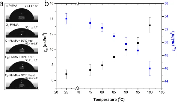
symmetric (absence of rectification). ... 61 Figure 2.3 Schematic showing the interfacial tensions in Young’s equation ... 62 Figure 2.4 Variation of the water contact angle (a) and surface tension forces (b) with
temperature for O2-PMMA. Planar PMMA pieces were activated using an O2 plasma with the
following conditions; power level of 50 W, 5.5 sccm gas flow rate and treatment time of 35 s. Each reported value represents the average of five values measured at different positions on the substrate and the vertical bars represent one standard deviation unit. ... 63 Figure 2.5 Zisman plot for u-PMMA (black trace) and O2-PMMA (red trace) measured with
water (γlv ~ 72.80 mJ/m2), glycerol (γlv ~ 64.00 mJ/m2) and DMSO (γlv ~ 43.54 mJ/m2). Each
Figure 2.6 Bar graphs showing (a) O/C and (b) N/C ratios for different surface modification schemes for both u-PMMA (unmodified) and O2-PMMA (plasma treated PMMA) obtained from
XPS data. Deconvoluted C1s spectra for (c) u-PMMA, (d) O2-PMMA and (e) NH2-PMMA.
PMMA peaks were labeled and assigned to the polymer’s monomer. Spectra for the plasma activated PMMA contained an additional peak for carboxyl functionalities and the amine-modified surface showed the presence of two peaks corresponding to the C-N bond of an amine and amide. (f) XPS survey spectrum of u-PMMA (black trace), O2-PMMA (red trace) and NH2
-PMMA (blue trace) nanoslits. (g) N1s deconvoluted spectrum showing two forms of nitrogen atoms. The insert shows the chemical structure of the aminated PMMA surface with the
nitrogens labeled N1 and N2. ... 66 Figure 2.7 ATR-FTIR spectra for (a) untreated (b) plasma-treated and (c) amine-modified PMMA. ... 69 Figure 2.8 AFM characterization of a PMMA nanofluidic device with 1 µm x 50 nm nanoslit (a) for: (b) u-PMMA; (c) O2-PMMA; and (d) NH2-PMMA. The image shown is 4 µm x 500 nm.
The measured root-mean-square (RMS) surface roughness was 0.80 nm, 0.95 nm and 1.03 nm, respectively, for these three devices. Also shown are AFM images for planar PMMA; (e) u-PMMA (f) O2-PMMA and (g) NH2-PMMA. Images on the planar PMMA were scanned over an
area of 3.5 × 3.5 µm. ... 70 Figure 2.9 (a) Schematic showing the experimental setup for measuring the resistance of the nanochannels. The nanofluidic device was interfaced to an Axopatch 200B amplifier connected to a Digidata 1440A and computer for readout. Each nanochannel of the array was assumed to have the same geometrical size. (b) Diagram showing the voltage drop and resistances across micro- and nanochannels. (c) Current versus time trace showing the current generated across a nanoslit arising from the replacement of a low ionic strength buffer (0.05 M KCl in 10 mM Tris buffer) with a higher ionic strength buffer (0.1 M KCl in 10 mM Tris) for an O2-PMMA nanoslit.
Buffer replacement within the nanoslit arose from the EOF associated with the device... 72 Figure 2.10 Conductance plots obtained from surface modified devices consisting an array of (a) four nanoslits (each 1 µm wide, 50 nm deep and 22 µm long), and (b) seven nanochannels (each 120 nm wide, 120 nm deep and 45 µm long) square and circle markers represent the data
obtained for the plasma and amine modified surfaces, respectively. The solid blue line represents the trace of the theoretical bulk conductance calculated with equation (2). Each data point
represents an average of five measurements with a scatter in the data within 5-8% of the mean value. From the graph, the effective surface charge density as calculated from the transition concentration, ct, was 38.2 mC/m2 for plasma treated nanoslit, 28.4 mC/m2 for amine treated
nanoslit, 40.5 mC/m2 for plasma treated nanochannel and 22.9 mC/m2 for the amine treated nanochannel. ... 77 Figure 2.11 Plot showing the effect of pH on the surface charge density σs, in plasma and amine
initial molecule length of 11.25 ±1.68 µm (calculated from n=20 events). However, when the voltage was turned off, the DNA relaxed to its equilibrium length. (b) Histogram of the measured end-to-end length of relaxed λ-DNA molecules confined in the PMMA nanochannel. The
average equilibrium length determined by the Gaussian curve fit (black line) was ~ 6.88 ±0.43 µm. Representative frames of fluorescently stained λ-DNA molecules translocating through a 100 nm × 100 nm plasma modified PMMA nanochannel and imaged in (c) 0.5× and (d) 2× TBE buffer at 80 V/cm and 120 V/cm, respectively. The time between frames is approximately 20 ms and scale bars are 10 μm. (e) Plots of DNA apparent mobility against the electric field strength for DNA translocation through the single nanochannel filled with 0.5× (black markers) and 2× (red markers) TBE buffer. Error bars represent the standard deviations in the measurements (n = 10) ... 83 Figure 2.13 Representative frames of translocation events of λ-DNA in amine modified
nanofluidic devices in the presence of a bias electric field (20 V) in a 2X TBE buffer (pH ≈ 10). ... 87 Figure 3.1 (a) Schematic illustration of the device assembly using the thermal press instrument. (b) Temperature-pressure process profile showing the six stages for the bonding cycle. ... 101 Figure 3.2 (a) Plot of the variation between the contact angle and RF power of the oxygen plasma at 10 sccm gas flow and a constant exposure time of 10 s. (b) Plot of the relationship between the water contact angle (black trace) and the RMS roughness (blue trace) versus the plasma exposure time at 50 W for 10 sccm gas flow. (c) Effect of ageing under room temperature conditions on the water contact angle of treated COC cover plate surface for plasma treatments condition of 50 W at 30 s under 10 sccm oxygen flow rate. (d) Water contact angle
measurements on the PMMA substrate under different surface modification conditions with and without the COC cover plate. (‘U-PMMA’ is untreated PMMA substrate, ‘PL-PMMA’ is plasma treated PMMA substrate, ‘UV-PMMA’ is UV-activated PMMA substrate,
measurements with a scatter in the data within 5-8% of the mean value and the solid black line represents the trace of the theoretical bulk conductance. (c) Plot showing the relationship
between the conductance and the electrolyte pH for the assembled hybrid devices before (black) and after (red) UV activation. 10-4 M KCl solution adjusted to pH between 5.01 and 9.09 was used in the study... 116 Figure 3.5 AFM profile of a nanoslit in a silicon (Si) master (red trace) and positive structure in the UV resin stamp (black trace) showing the replication fidelity in the structure. ... 118 Figure 3.6 (a) Upper panel - AFM image of the first UV resin stamp produced from the Si master. Lower panel – Box plots of the stamp height measured with the AFM from 20 stamps produced from a single Si master. (b) Upper panel – AFM image of the first PMMA device generated after thermal imprinting using a UV-resin stamp. Lower panel – Box plots of the nanoslit depth measured with AFM from 20 substrates produced from a single UV-resin stamp. Both images reveal ~100% replication fidelity of nanostructures from the master to stamp to substrate. ... 118 Figure 3.7 (a) AFM scan (and SEM image insert) of the UV curable resin stamp possessing the positive tones of the 2-D nanochannels. Channels were imprinted into PMMA with ~100% replication fidelity and the dimensions (width × depth) were nc1 ≈ 300 × 200 nm, nc2 ≈ 250 × 155 nm, nc3 ≈ 190 × 95 nm and nc4 ≈ 150 × 60 nm and nc5 ≈ 110 × 25 nm. (b) Bar graphs showing the signal-to-noise ratio (SNR) at 2 s exposure time for the devices with untreated PMMA substrate enclosed with a plasma treated COC cover plate, U-PMMA/(PL-COC), and plasma treated substrate enclosed with a plasma treated PMMA cover plate, PL-PMMA/(PL-PMMA) filled with 5 mM FITC solution. The error bar represents the standard deviation in measurements from ten separate devices. (Insert shows the unprocessed image of the seeding test for U-PMMA/(PL-COC)). The hybrid devices showed a background that was ~56% lower than that of the non-hybrid devices. (c) Unprocessed representative frames of T4 DNA molecules stretched in the enclosed nanochannels in the hybrid devices. Images were acquired at 10 ms exposure time with the driving field turned-off. (Note that nc6 ≈ 35 × 35 nm). (d) Log-log plot showing the T4 DNA extension as a function of the geometric average depth of the
nanochannels. The DNA extension was normalized to a total contour length (Lc) of 64 µm for the
dye labelled molecules. The red and blue dashed lines are the deGennes and Odijk predictions, respectively, with the respective equations inserted. The black solid line is the best power-law fit to the data points obtained from the nanochannels with an average geometric depth range of 53 nm to 200 nm. ... 119 Figure 3.8 Graph showing the relationship between the translocation velocity (cm/s) and the field strength (V/cm) of λ-DNA translocating through the hybrid devices before and after activation with UV light. Each data point represents the mean of 20 events per device measured in 2× TBE buffer. ... 120 Figure 4.1 (A) Microelectrode mask (insert: connecting points to nanoelectrodes) (B)
Figure 4.2 Representation of the nanofluidic device with an abrupt nanochannel inlet. The panel on the right is the enlarged view of the nanochannel/microchannel interface showing the capture zone with radius r* and electrokinetically transported DNA molecules. ... 136 Figure 4.3 (a) On axis SEM image of the pillar inlet. (b) Frames showing the motion of DNA through the nanopillar array showing gradual unravelling by hooking around the pillars. (c) SEM of the grooved inlet and (d) a montage of typical DNA motion inside the grooved inlet. (e) Off axis SEM of the trapezoidal funnel inlet taken at 52o. (f) The fluorescent image DNA captured in the inlet. (g) On axis SEM image of the 3-D funnel inlet, and (h) frames of the DNA migrating from the inlet into the nanochannel. (Insert shows the off-axis SEM image of the 3D-funnel taken at 40o. The funnel was ~35 µm long, 3.7 µm wide and 2.2 µm deep at the base). ... 138 Figure 4.4 (a) The normalized capture rate for various inlet structures under a voltage of 0.5 V. (b) Simulated electric field strength distribution at each inlet structure. An electric potential of 1 V was applied across all inlets ... 139 Figure 4.5 (a) Representation of the mode of measurement of the longitudinal blockage current. (b) Off-axis SEM image of the device acquired at 52° showing the assess microchannels and the connecting nanofluidic structures. (c) High magnification view of nanopillar array inlet,
nanochannel and groove outlet. (d) High magnification view of the connection between the nanochannel and the nanopillar input. ... 140 Figure 4.6 (a) Series of frames of seven DNA translocation events and the corresponding
Figure 4.12 (a). Diagram showing the principle of FIB milling. Ga+ induces the ejection of substrate materials in the form of secondary atoms, ions and electrons simultaneously creating a nanotrench. (b) Variation of the Beam diameter with the beam current at 30 kV obtained from FEI Helios operational manual. ... 151 Figure 4.13 Schematic depicting the cross-section of the (a) nanoelectrode and (b) Quartz surface. Both regions were coated with Al prior to FIB milling. The nanoelectrode consists of 40 nm Au and 10 nm Cr adhesion layer. After milling, the final nanogap width is denoted as x1 and
the depth of penetration of the trench into the base SiO2 layer is denoted as z. The width of the
nanochannel fabricated in quartz is denoted as x2 with the depth denoted as h2. (c) Variation
between the nanogap width and the nanochannel width. (d) Variation between the penetration depth in the base SiO2 layer beneath the nanoelectrode and the depth of nanochannel in the fused
silica after FIB milling. The intercept on the horizontal axis shows the depth of the nanochannel in fused silica when the nanogap depth is exactly 50 nm. (e) Off-axis (52o) SEM images of cross-sections of the FIB milled nanochannels in fused silica. The widths × depths are 165 × 240 nm, 130 × 187 nm, 95 × 150 nm, 80 × 110 nm and 50 × 52 nm (from left to right) ... 152 Figure 4.14 (a) SEM image of the FIB milled 1-D dual nanoelectrode device. The panel below shows the on axis image taken at a higher magnification. The measured nanogap width was ~54 nm and the nanochannel width was 43.5 nm. (c) SEM images of the FIB milled 2-D dual nanoelectrodes separated by a distance of 40 µm and connected by a 45 × 45 nm nanochannel with a 3D funnel input populated with nanopillars at the entrance. The top panel shows the nanogap ~30 nm × 50 nm and the bottom panel shows the nanopillars, ~800 nm in diameter spaced by ~150 nm... 153 Figure 4.15 Equivalent circuit for the dual nanogap integrated device. (Rne is the Resistance of
Nanoelectrodes; RN(ent) and RN(ex) are the Resistance of Entrance and Exit Nanogaps respectively;
Cne is the Capacitance on the nanoelectrode surface in contact with the buffer ions; Rm =
Resistance of access microchannel; R1 and R2 the Resistances of connecting nanochannel and R3,
in our case, is the resistance of the entrance funnel and the short exit nanochannel. ... 154 Figure 4.16 (a) Interconnect diagram of the experimental setup showing the nanofluidic device, high bandwidth current-voltage (I-E) amplifiers, opto-isolators and digitizer. (b) Simplified circuit diagram and (c) photograph of the home built I-E amplifier. (d) Bode plot showing the frequency response of the homebuilt amplifier compared to the commercial axopatch 200B amplifier measured using a digital oscilloscope. The graph shows a bandwidth of ~103 kHz and ~70 kHz for the homebuilt and commercial, respectively. ... 155 Figure 4.17 Current voltage plots measured (a) longitudinally along the nanochannel/input funnel and (b) transversely across the nanogap with 2× TBE in the absence of a longitudinal field ... 157 Figure 5.1 Schematic of the nanosensor that accepts dsDNA input molecules and deduces their primary sequence by the sequential clipping of the input dsDNA molecule using an exonuclease enzyme. The single dNMPs generated are moved through a nanochannel that produces a
from the appropriate polymeric material to suit the application need and the structures produced via micro- and nano-replication technologies. The nanosensor uses electrical signatures to monitor the input of dsDNA, immobilized exonuclease to complex the dsDNA, entropic traps to stretch the dsDNA and identify the clipped dNMPs using flight-times through 2D nanochannels. ... 167 Figure 5.2 (a) Illustration, (b) SEM image and (c) Equivalent circuit of the multi-structured 3D Funnel/Entropic trap/Nanopillar device. Nanochannels are represented as resistors and the entropic trap is represented as a capacitor. (d) Frames showing the translocation of lambda DNA through the device. (e) and (f) shows the histograms of the resident time and translocation time of the migrating DNA, respectively under a 0.1 V driving voltage ... 169 Figure 5.3 (a) Optical set-up of the imaging system. The Gaussian beam from the Laser
(Nd:VYAG (λex = 532 nm; P = 0.01-5W; 2.2 mm beam diameter) was initially passed through a Neutral density filter (NDF) then expanded 10 times with a Kaplerian beam expander (focal lengths are 20mm and 200mm for L1 and L2 plano-convex lenses, respectively) and the wings knocked out with a shutter that ensures uniform laser intensity in the field of view and complete back-filling of the objective (OBJ). The beam was focused through an iris into the back end of a 100x oil immersion objective lens (OBJ) using lens (L3) through a 532nm laser line filter (F1) and the reflection from a dichroic filter (DF). A collimated laser beam is impinged upon the polymer nanofluidic device. The fluorescence signal generated from the single molecule was collected by this same objective, passed through the DF and spectrally selected using a long pass filter (F2). A mirror was used to steer the fluorescence signal onto an EMCCD after through a band-pass filter (F3) and focused using lens (L4). (b) 3D surface plot of the fluorescent image of the dye labelled nucleotides viewed under the system... 170 Figure 5.4 Variation between the electrical signal-to-noise (SNR) ratio and the nanogap size for different nanoelectrode areas for single mononucleotide units at 500 mV bias. As the
LIST OF SCHEMES
Scheme 2.1 Protocol for the surface modification of PMMA with (a) carboxyl groups by plasma activation, and (b) amine groups by chemical reaction with ethylenediamine through EDC
coupling chemistry to the plasma activated PMMA………..………..54 Scheme 4.1 The five processing steps involved in the fabrication of the dual electrode
LIST OF ABBREVIATIONS
AC Alternating Current
B Bandwidth (Hz)
Ceq Equivalent Concentration
Ci Bulk ionic Concentration of solution (mol/dm3)
Cyt c Cytochrome c
DC Direct current
DL Diffuse Layer
DLVO Derjaguin, Landau, Verwey and Overbeek
DNA Deoxyribonucleic acid
DRIE Deep Reactive Ion Etching
Du Dukhin number
E Electric Field strength (volts per centimeter or V/cm)
EDL Electric Double Layer
EDTA Ethylene Diamine Tetra Aceticacid EKP Electrokinetic Phenomena
EOF Electroosmotic flow
eV electron Volt (1 eV = 1.6026 × 10⁻¹⁹ J)
F Faraday’s Constant (96,485 C/mol)
Fd Drag Force (N)
Fe Electrical force (newton/N)
FIB Focused Ion Beam
G Conductance (Ω-1 or siemens) g Acceleration due to gravity (9.8ms-2)
GB Conductivity of Buffer
I Ionic strength of electrolytes
Icond, bulk Conduction Current from Bulk solution conductivity (A)
Icond, surf Conduction Current from Surface conductivity (A)
It Tunneling Current
kB Boltzmann constant (1.38 × 10⁻²³ JK-1)
lp Persistence length (nm)
Lcont Contour length
m Mass of electron (9.10938188 × 10⁻³¹ kg)
NA (mol-1) Avogadro’s number of molecules /ions (6.02214 × 10²³)
PDMS Poly (dimethylsiloxane)
Q Volume Flow rate (liter per min) R (JK-1mol-1) Molar Gas constant
RMS Root-Mean-Square
SL Stern Layer
T Kelvin Temperature (Kelvin or K)
TBE Tris(hydroxymethyl)aminomethane-borate-EDTA ui Effective Ionic Mobility (m2/sV)
ui∞ Absolute Ionic mobility
vep Electrophoretic velocity
zi Ionic Charge
ΔG Change in conductivity
Δp (Atm) Pressure drop ΔV (volts) Voltage drop
ε0 Electrical permittivity of vacuum
εe Electrical Permittivity of a medium
εr Relative dielectric constant
εw Dielectric permittivity of solvent (usually water)
ζ (mV) Zeta Potential
η Dynamic Viscosity of solution
κ Electrical Conductivity (siemens per centimeter or S/cm) κb Bulk electrolyte conductivity (Ω-1m-1)
κd Debye-Hϋckel parameter
κs Surface conductivity (Ω-1m-1)
λd Debye Length
μeof Electroosmotic flow mobility (cm2 V-1 s-1)
μep Electrophoretic mobility (cm2 V-1 s-1)
νeof (cms-1) Electroosmotic Flow Velocity
ρ (Ω cm) Resistivity at a temperature T σ (gcm-3
) Density
CHAPTER 1: NANOFLUIDICS FOR BIOPOLYMER ANALYSIS
Introduction
Many fundamental processes in biology, for example, information storage, transcription, translation, gene regulation, mitosis, and cell communication occur in the micrometer to
nanometer scale (Doherty, '03; Gilges, '94; Hwang, '08; Shenton, '01). Using micro- and nanofabrication technologies developed for the microelectronics industry, new analytical tools on these length scales have been readily developed for single molecule studies of biomolecules at a size-scale comparable to their intrinsic dimensions.
The miniaturization of analytical devices is an ongoing endeavor with the impetus focused on improving performance in a faster and cheaper fashion. The general benefits of miniaturization are the use of less reagents, parallel analysis, faster operation, and more sensitive detection (Vesel, '12). More interesting are the new qualitative possibilities that include: Single-cell analysis by integration of several biochemical steps into a micro Total Analysis System (µTAS); high-resolution analysis using local light sources and detectors or local electrical detection; and direct manipulation of relevant entities such as proteins, nucleic acids, bio-molecular complexes and organelles (ribosomes and mitochondria) in addition to whole cells.
at the single cell level (Beech, '12; Gilges, '94; Hwang, '08), and the separation of biomolecules (Effenhauser, '97; Jönsson, '10) many fundamental biological processes, such as the epigenetic and genetic control of single cells, have been reported to occur at the molecular level (i.e., nano-scale). Hence, the emergence of nanofluidics – the study of fluid flows in structures with at least one dimension approaching the nanometer scale (Reisner, '05; Roy, '10).
While microfluidics have been reserved for flows in channel with dimensions ranging from 100 nm to 100 μm, nanofluidics entails flow in channels with dimensions between 1 and 100 nm (Abgrall, '08). Although, in the past, scientists have studied transport properties on fluids in the nanoscale, it is not until the last several years that this field was coined (Eijkel, '05). The invention and wide availability of many new technological tools like atomic force microscope (AFM) (Pennathur, '07) and scanning tunneling microscope (STM) (Bensimon, '95; Binnig, '82) (both for inspection and creation of nanostructures), electron (Broers, '96) and ion-beam
lithographs (Dobisz, '91; Marrian, '92) and the development of new nanomachining techniques like soft lithography (Qin, '10; Whitesides, '05), bottom-up assembly methods (Du, '08) and surface science apparatus (SFA) (Derjaguin, '54) has made the study and application of
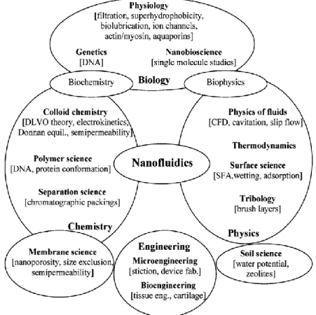
nanofluidics much more accessible. Fluid conduits with at least one dimension from 1 nm to 100 nm that exist in nature include nanopores in zeolite crystals (Salavati-Niasari, '08) and nuclear membranes of biological cells to larger openings in the silica frustules of diatoms (Mazumder, '10; Yamanaka, '08). Also, molecular dynamic (MD) simulations have become a useful tool for elucidating the molecular discreteness, ion transport and fluid flow within nanochannels (Chen, '08; Li, '10). Figure 1.1 shows a number of classical disciplines where nanofluidics is currently being applied.
interactions. As the dimensions of fluidic channels approach the nanoscale, changes in the dominating forces as well as the physics of the processes for fluid/particle transport becomes more pronounced. These changes, as reported by Gad-el Hak (Conlisk, '05; Gad-el-Hak, '99), arise from an increase in the surface-to-volume ratio as dimensions are scaled down.
Consequently, forces resulting from pressure, inertia, viscosity or gravity that usually plays the dominant role in macroscopic flows may become irrelevant in micro/nanofluidic systems while interfacial forces, like surface tension, become immensely dominant. As a result, it becomes difficult to transport materials (like water, ions and particles) in nanoscale systems via pressure driven flow and easier to utilize electrokinetic (EK) transport.
Figure 1.1 Classical disciplines relevant to nanofluidics and the different phenomena. (Reproduced from
Eijkel et al., Microfluid. Nanofluid. 2005, 1, 249 – 267)
height of the channel approaches 10 nm, for a flow-rate of 1 μl/min, the pressure drop increases from 0.006 to 3 atmospheres (~50000%), while the voltage drop increases by ~560% from 0.05 V to 0.33 V. In reality, a relatively bulky pump would be required to deliver this low flow rate at such a huge pressure drop. However, the magnitude of the voltage drop makes the electrokinetic driven flow more practical.
Figure 1.2 Required pressure drop and voltage drop for nanochannels with different channel heights.
Nanochannel length and width are 3.5 μm and 2.3 μm, respectively, zeta potential is -11 mV for 1M NaCl solution. (Reproduced from Conlisk, A.T. Electrophoresis 2005, 26, 1896-1912)
1.1 Parameters in Nanofluidics
1.1.1 Electric Double Layer (EDL)
surface. Outside this layer, another layer of mobile cations is generated as well. These two layers form a single shielding layer that is usually referred to as the Electric Double Layer (EDL) or Debye Layer. Typically, the Gouy-Chapman-Stern model (GCS) is used to describe the EDL (J.Lyklema, '95). As shown in Figure 1.3, the GCS model consists of two layers – Stern layer (SL) and diffuse layer (DL). The SL is the region next to the solid surface and ions in the SL are bound near the surface due to adsorption and Coulomb interactions while the DL is the mobile region next to the SL.
The EDL thickness is an important electrokinetic parameter, in the nanofluidics. For a channel filled with a symmetrical 1:1 electrolyte such as KCl with ionic concentration c, the EDL thickness or λD can be represented as;
λD= (ϵ0ϵrRT
2F2c ) 1/2
(1)
where R is the gas constant (J·mol-1K-1), ϵ0 is the permittivity of vacuum (F·m-1), ϵr is the
dielectric constant of the medium, F is the Faraday constant (C·m-1), and T is the temperature (K). λD can range between 0.1 and100 nm for electrolyte concentrations between 10 and 0.01
mM.(Abgrall, '08)
The ratio of λD to channel height, h has been used to describe the state of electroneutrality
of the bulk solution within the channel. For channels with heights of several micrometers to ~150 nm, it applies that λD
h
≪1
. In this case, the solution towards the center of the channel that is away from the EDL is electrically neutral, i.e., equal concentration of co-ions and counter-ions within the channel, with a neutral electric potential (see Figure 1.4A). However, in the case where the channel height is on the order of the EDL thickness, that isλDthe EDL leading to an excess of counter-ions in the channel and loss of electroneutrality (see Figure 1.4B).
Figure 1.3 Model of the Electric Double layer at a Solid-liquid interface at a negatively charged solid
surface/channel wall. (Reproduced from Lyklema J., Vol. 2 – Solid-Liquid Interfaces. First Edition ed.; Academic Press: London England, 1995)
1.1.2 Zeta Potential (or Electrokinetic Potential)
The zeta potential ζ, which measures the electric charge developed on a solid surface in contact with an aqueous solution, is the electric potential at the boundary dividing the SL and DL, also known as the shear plane (see Figure 1.3). Typically, the values of ζ can vary between -200 mV to +-200 mV depending on the chemistry of the solid/liquid interface. Also, it is a
measureable zeta potential. Sze et al. (Sze, '03) reported that the ζ-potential for surfaces in KCl and LaCl3 aqueous solutions varied between -88 to -66 mV and -110 to -68 mV for glass and
PDMS surfaces, respectively, independent of the channel size and driving voltage.
Figure 1.4 Illustration of differences in the electric potential and ionic concentrations for (A) Channels
filled with moderately to highly concentrated electrolyte (and/or large channel height [h > λD]) and (B) Channels filled with low concentrated electrolyte (and/or small channel height [h ≤ λD]). (Reproduced from Lyklema J., Vol. 2 – Solid-Liquid Interfaces. First Edition ed.; Academic Press: London England, 1995)
The ζ-potential has been an important parameter in a number of applications (Erickson, '03; Ross, '01) like characterization of membrane efficiency (Reischl, '06), biomedical polymers (Werner, '99) and electrokinetic transport of particles and blood cells (Minerick, '02). Typically, it has been evaluated indirectly from other electrokinetic parameters (Alkafeef, '06; Oddy, '04; Werner, '98).
1.1.3 Electrical Conductivity
The total electrical conductivity of an electrolyte confined in a fluidic channel is a sum of the surface and bulk electrical conductivities arising from the electrically-driven motion of ions under the influence of an external electric field.
The bulk conductivity, κB can be computed with the Faraday’s constant, (F = 96,485
C/mol), the effective mobility ui, concentration ci, and charge zi of the ions present in solution
using the equation (Bard, '01) (Coury, '99);
κB =F∑ ||i| zi| uici (2)
The bulk conductivity of the solution is also represented as the product of the total ionic concentration of ions in a solution and the molar conductivity, Λ.
κB = Ci Λ (3)
where; Λ = z+ λ+ + z- λ-. The molar conductivity of a dissociable solute increases with ionization,
depending on the pH, and decreases by any interaction with other solutes and surfaces.(Brody, '04)
The surface conductivity, κS, is an additional component from the fluids tangential to the
charged surface and originates from excess counter-ions in the EDL region. Ions from the electrolyte are attracted towards the wall by electrostatic forces induced by the surface charge. Higher concentrations of ions towards the wall lead to a high surface conductivity. Under thin EDL conditions, i.e. high electrolyte solutions, the contribution of κS is minimal and negligible.
However, under low electrolyte concentrations or high surface charge densities, the EDL thickness increases and κS contributes significantly to the total conductivity. A more detailed
description of κs has been reported by Lyklema et al. (J.Lyklema, '95; Lyklema, '98). Although it
The surface conductivity, just as well as the zeta potential, is a very important interfacial electrokinetic property relevant to a number of natural phenomena, such as electrode kinetics, electrocatalysis, corrosion, adsorption, crystal growth, colloid stability and flow characteristics of colloidal suspensions and electrolyte solutions through porous media and microchannels. It is therefore important to measure κs in studies of electrokinetic phenomena. Specific surface
conductivity values reported for water in glass capillaries is on the order of 10−9 ~ 10−8 Ω-1m-1 (Gu, '00). Researchers have successfully determined the magnitude of the surface conductivity for other important materials (Alberghi.Je, '66; Perevert.Vd, '72; Revil, '98; Stec, '10).Bikerman (Bikerman, '33) was the first to lay down a theoretical prediction for computing the surface conductivity. Squires et al. (Squires, '04) reported the mathematical representation as;
κS = 4 κB λD (1 + m) Sinh2 (
zi qi ζ
4 k T) (4) where m characterizes the contribution of electro-osmosis to the motion of ions within the DL, k is the Boltzmann’s constant and T is the temperature.
1.1.4 Electroosmotic Flow (EOF)
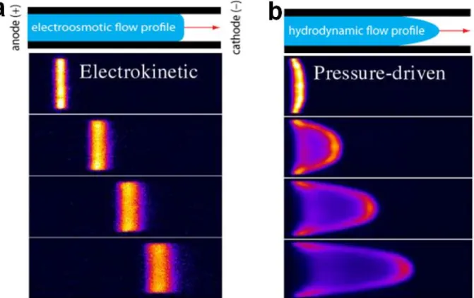
molecules inducing a bulk flow of ions under the influence of the external electric field. This is referred to as the electroosmotic flow (EOF) and is illustrated in Figure 1.5a. For a thin EDL or large channel height, the EOF has a ‘Plug-like’ (or flat) profile. Unlike the typical hydrodynamic flow, which has a ‘parabolic’ profile (Figure 1.5b), this flat profile has been reported to result in high-efficiency electrokinetic separations (Jorgenson, '81; Paul, '98; Rice, '65).
Figure 1.5 Comparison between the (a) plug-like (electrokinetic) and (b) hydrodynamic (pressure driven)
flow profiles in a negatively charged channel wall imaged by nonintrusive, caged-fluorescence technique. (Reproduced from http://microfluidics.stanford.edu/Projects/Archive/caged.htm)
The direction of the EOF depends on the type of charge (positive or negative) on the channel wall. For a negatively charged wall, as shown in Figure 1.5, under the influence of an external field (E), the bulk liquid flows towards the cathode while it is reversed in a positively charged wall. The mathematical representation of the EOF velocity, veof, shown in equation 5
veof = - ϵrηE ζ (5)
Because the EOF mobility is the ratio of the EOF velocity and the applied field strength (i.e. µeof
= veof /E),
µeof = - ϵr ζ
η (6)
It can be deduced from equation 6 that μeof depends on channel wall conditions,
properties of the solution (viscosity and ionic strength), pH and composition of the background electrolyte. Typically, parameters that influence the charge on the channel wall will similarly affect the zeta potential and EOF mobility.
1.2 Nanoscale Phenomena
Electrophoresis performed on the nanoscale utilizes channels with dimensions around 150 nm or less. This introduces many unique phenomena since important length scales are now comparable to the channel dimensions including the electrical double layer (EDL), characterized by the debye length. Furthermore, since the reduction in channel size increases the surface area to volume ratio, surface reactions are enhanced and the surface roughness begins to contribute to the overall flow pattern (Baldessari, '06; Movahed, '11; Pennathur, '05; Piruska, '10; Schoch, '08; Xuan, '06; Yuan, '07). Previous theories on the electrokinetic flow in microchannels utilizing Boltzmann distributions and the Poisson-Boltzmann equation cannot be directly applied to nanochannels since the concentration of co- and counter ions in nanochannels are unequal and significant EDL overlap can be easily observed (Movahed, '11). This requires the development of new theories to explain electrokinetic flows in nanochannel channels.
Xuan, '06; Yuan, '07). This non-uniformity has drastic effects on dispersion within nanochannels due to the fact that analytes spend a significant time migrating through the EDL (Baldessari, '06). Counter-ions are more attracted to the wall and their flow is impeded, while co-ions are repelled from the wall and are transported faster (Piruska, '10; Yuan, '07). In addition to enhanced
separation based on charge, separation based on size can be achieved since smaller molecules approach the wall and experience slower flow profiles than larger molecules (Piruska, '10). At this size scale, the kinetics of adsorption and desorption approaches the time required for diffusion forcing the consideration of wall adsorption; hence, the possibility of performing chromatographic separations in nanochannels (Baldessari, '06).
Furthermore, concentration polarization is a unique phenomenon observed at the interface of microchannels and nanochannels due to the increased flux of ions within the nanochannel from to the enhanced transport within the EDL of selective ions (Baldessari, '06; Piruska, '10; Yuan, '07). When the EDL spans the dimensions of the nanochannel, counterions are able to pass through the EDL while co-ions are excluded resulting in the accumulation of counter-ions and co-ions at the inlet and outlet of the nanochannel with an increased transport of divalent counterions. Doubly charge ions will be strongly attracted to the double layer; hence at the same ionic strength, the total ionic concentration of divalent counterions in the nanochannel becomes higher. Therefore, at low ionic strengths (increased EDL thickness) and non-adsorbing conditions, there will be an increase in the electric current and fluid transport while at high ionic strengths and adsorbing conditions the ζ-potential decreases leading to a decrease in the
streaming current and fluid transport fluid (Yuan, '07).
viscosities to be as high as 1.3 depending on the material of the channel wall, spatial size and shape of the channel, the ionic concentration, zeta potential, temperature, dielectric constant and other properties of the liquid. This increase in viscosity leads to an apparent decrease in the EOF within nanochannels.
1.3 DNA Molecule as a Model Polymer in Nanofluidics
In their 1953 article published in Nature entitled ‘Molecular Structure of Nucleic acids’ (Watson, '53), James Watson and Francis Crick described the Deoxyribonucleic Acid (DNA) as a long biopolymer composed of repeating units called nucleotides with two negatively charged backbones intertwined in a double helical structure. As shown in Figure 1.6, each backbone is coiled around the same axis and has a pitch of 34 Å (3.4 nm) and a radius of 10 Å (1.0 nm). In living cells, the DNA is organized into chromosomes and packaged by histones and is
responsible for the encryption and transmission of hereditary information. A single nucleotide unit of DNA is composed of a nitrogenous base, a five-carbon 2’-deoxyribose sugar and one to three phosphate groups. These phosphate groups can form bonds with carbon 2, 3 or 5 of the sugar groups. A set of 46 chromosomes make up the total genome and contains 3 billion base pairs, which extends approximately 1.8 m in length (J.Lyklema, '95; Venter, '02; Venter, '01; Venter, Adams, , '01). When dealing with a DNA molecule and its associated number of degrees of freedom, it is useful to treat the behavior of this polymer by statistical quantities. The mean-square end-to-end distance (or displacement length) RF2 and the mean-square radius of gyration,
RG2 are two important quantities in conformational statistics of the polymer chains that provide
Figure 1.6 The DNA molecule is a long biopolymer which consists of several hundred million base-pairs (bp) with each base-pair contributing 0.34 nm to the total length of the molecule. The backbones of a dsDNA are held together by the bases that pair-up in a manner in which the nucleotides Adenine (A) binds to Thymine (T) and Guanine (G) binds to Cytosine (C) following the Watson-Crick based-pairs (bp). The DNA is tightly wound around proteins called histones and packaged into the nuclei of a cell in the form of chromosomes. (Reproduced from www.virtualmedicalcentre.com)
Although, the biological properties of a DNA molecule are very complex, the physical properties involved in the molecular dynamics can be described by three parameters; the contour length, Lc, persistence length, lp and the effective width, weff (Reisner, '05). The contour length
refers to the total length of the DNA when it is fully stretched. As stated by Watson and Crick, each base pair contributes 0.34 nm to the full contour length. Due to its double helical structure, the DNA molecule becomes locally rigid (Manning, '88).
hydrodynamic theory measurements of intrinsic viscosity and the sedimentation coefficient as reported by Hays et al (Hays, '69). On length scales smaller than lP, a DNA molecule is
considered rigid, while it is flexible at length scales larger than lP. The intrinsic persistence
length and width, w0 of dsDNA in 0.1 M aqueous NaCl are ~50 nm (150 bp) and 2 nm,
respectively (Manning, '06). The effect of self-avoidance on flexible polymers that are freely coiled in solution was first understood by Flory (Baumgärtner, '82; Orland, '94) and later generalized to the semi-flexible case by Schaefer et al. (Schaefer, '80) Flory-Pincus represented the RF for a real polymer by the equation;
RF ≅ (lp weff)1 5⁄ Lcont3 5⁄ (7)
The radius of gyration relates to RF by;
RG ≅ R√F6 (8)
Based on the values reported by Reisner et al. (Reisner, '07), for 0.5× TBE buffer with 20 mM ionic concentration, wo is 3 nm and weff was estimated to be 12 nm. It is known that the
intercalation of YOYO-1 dye to dsDNA causes an extension in its contour length. At a dye concentration, of 1 dye molecule per 5 base pairs, a 20% increase in the contour and persistence length was estimated. Therefore, the adjusted persistence length will be 53 nm and the contour lengths of lambda (λ) and T4 DNA will be Lc (λ) = 20 μm and Lc (T4) = 64 μm. Therefore, based
on equations 7 and 8, the radii of gyration will be approximately ~560 nm and 1140 nm for λ and T4 DNA, respectively, in 0.5× TBE buffer.
1.4 DNA Confinement in Nanochannels
of its full contour length (Reisner, '07). Confinement elongation of genomic-length DNA has several advantages over alternative techniques for extending DNA, such as flow stretching and/or stretching relying on a tethered molecule. Confinement elongation does not require the presence of a known external force because a molecule in a nanochannel will remain stretched in its equilibrium configuration allowing for continuous measurement of length (Tegenfeldt, '04).
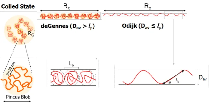
Figure 1.7 Representation of DNA molecule in the microchannel (coiled state) in a nanochannel with the
average dimension greater than (deGennes regime) and less than (Odijk regime) the persistent length of dsDNA.
In confined spaces, where RG is much larger than the geometrical average depth, Dav, of
the nanochannel, the number of available configurations of the polymer reduces. Two main confinement regimes exists and depending on differences between the average depth and persistence length lp. When Dav >> lp, the molecule is free to coil within the nanochannel and
stretching is entirely due to excluded volume interactions between different coiled segments of the polymer separated along the backbone. Coiling of the molecule can be envisioned to be broken up into a series of blobs with diameter Lb, while the stretching is a result of repulsion
confinement force is only a weak perturbation while each blob retains the property of the bulk polymer. This is diagrammatically illustrated in Figure 1.7. The extension length of the molecule, Rx, can be calculated using the equation;
Rx = Lc (weff lp
Dav2 ) 1 3⁄
(9)
where Dav = √D × h and is the geometrical average of the two confining dimensions in the
nanochannels.
As the channel width decreases and Dav << lp, the stretching is strictly not a result of
volume exclusion but an interplay between confinement and the intrinsic elasticity of the DNA. The strong confinement prevents the molecule from forming loops within the nanochannel. Back folding becomes energetically unfavorable and stretching becomes a result of deflection of the molecules in the channel walls. The average length between these deflections is of the order of the Odijk length scale λp ≅ (Dav2 lp)1 3⁄ . This regime is referred to as the Odijk regime (see Figure 1.7) (Odijk, '06; Odijk, '83). For a small average deflection, θ, Rx is represented as;
Rx = Lcont cos θ ≅ Lcont [1 - 0.361 (Dlav p )
2 3⁄
] (10)
1.5 Effects of Ionic Environment on DNA Molecules
interactions between charges separated by less than the Debye length in contour resulting in an increase in the persistence length to a new value for lp. The mechanisms of these interactions
determine the ionic strength variation of the extension over an ionic strength range. The Odijk-Skolnick-Fixman (Baumann, '97) equation based on single-molecule elasticity has suggested that the new persistence length of a DNA when in solution relates to the ionic strength of the solution by;
lp = lpo + 0.0324 MI nm (11) where lpo = high salt value of persistence length (≈ 50 nm). According to equation 11, lp is
roughly equal to lpo until the ionic strength drops below 10 mM. lp increases up to about 80 nm
between 10 mM and 1 mM.
Although, reports have shown that the extension of DNA in a nanochannel almost triples when the ionic strength is changed by two orders of magnitude, experiments have revealed that even over a range of 4 - 200 mM ionic strength, variation in the persistence length is not large enough to explain the observed extension of DNA. This is in contrary to a report by Krishnan et al. (Krishnan, '07) and explains why nanoconfinement of DNA is critical for enhanced
stretching.
1.6 Nanochannel fabrication
1.6.1 Nanochannel fabrication in inorganic substrates
Inorganic substrates like glass, fused silica and silicon have been widely used as substrates for the fabrication of nanofluidic devices due to their established surface chemistry, excellent optical properties and well-entrenched fabrication techniques (Chantiwas, '11). The most prominent techniques for the fabrication of nanochannels in inorganic substrates are the top-down direct writing using focused ion beam (FIB) (Menard, '11) or electron beam
lithography (EBL) (Broers, '96) followed by dry etching.
In the case of EBL, nanopatterns are initially defined in a thin layer of polymer resist using a beam of focused electrons then transferred to the underlying substrate after development and etching. EBL has been useful for the fabrication of features as small as 10 nm (Broers, '96) and with the combination of electron beam evaporation, have been used for the fabrication of nanometer sized metal electrodes (see left panel in Figure 1.8). On the other hand, nanochannels are fabricated with the FIB instrument by focusing a beam of high energy Ga ions, onto the surface resulting in the sputtering of atoms of the substrate (Menard, '11). Also, nanoelectrodes have been fabricated with the FIB by deposition using the gas injection system (Maleki, '09).
Recently, FIB was utilized for the fabrication of sub-5nm structures in fused silica substrate through a thick conductive metal layer using a 1.5 pA ion beam current (see right panel of Figure 1.8) (Menard, '11). Using EBL and/or FIB, several groups have developed nanofluidic devices in inorganic substrates for the analysis of biomolecules and the evaluation of transport phenomena in nanofluidic channels (Cabodi, '02; Levy, '10; Menard, '12; Menard, '13; Yang, '06). Though, both EBL and FIB are expensive, slow and impractical for large-scale
substrate and the capping layer (Tas, '02) and self-enclosing of nanochannels using a UV laser pulse (Xia, '08).
Figure 1.8 Left panel – Steps in the fabrication of nanogap detectors via (a) Fabrication of a single
nanofluidic channel on a fused-quartz substrate using EBL; (b) imprinting of a nanotrench into the resist layer, which is perpendicularly across the nanochannel, for a subsequent mental lift-off; (c) deposition of the metals in the nanotrench via the shadow evaporation with two symmetric tilted angles; (d) after a lift-off, a pair of metallic nanowires is formed across the nanochannel with a sub-10 nm breaking gap in the channel (see inset); and (e) after making final metal contacts, the nanochannel, nanowire, and nanogap are conformably sealed by a coverslip coated with a conformable layer. (Reproduced from Liang et al., Nano Letters 2008, 8, 1472-1476). Right Panel – FIB milling process scheme and subsequent fabrication steps. (a) Milling a nanochannel through the thick metal film. (b) Removal of the metal film using an etching solution. (c) Sealing of the micro- and nanochannels with a cover plate. (Reproduced from Menard et al., Nano Letters 2010, 11, 512-517).
1.6.2 Nanochannel Fabrication in Organic Substrates
Organic substrates useful for the fabrication of nanochannels include elastomers and thermoplastics.
1.6.2.1 Elastomeric Nanofluidic Devices
of an external load while the covalent cross-links help elastomers return to their original shape upon release of the load. Nevertheless, this property sometimes creates problems during the fabrication of nanochannels. Several efforts have been channeled towards overcoming or
harnessing the deformability of elastomers for the generation of functional nanochannels. In fact, the unwanted collapse, which has traditionally been regarded as a problem in microfluidic chips, has been exploited for the fabrication of nanochannels (Lasse, '08). Mills et al. (Mills, '10) found that when a sheet of PDMS was mechanically stretched, exposed to oxygen plasma or U/ozone, then released, sinusoidal wrinkle patterns were generated due to the change in surface stiffness and the need to release strain. The authors modulated the amplitude of the wrinkle structures by controlling the applied strain, replicated the pattern into a UV-curable epoxy resin and
transferred into PDMS. The resulting nanochannel was triangular with the base length and height of 688±79 nm and 78±18 nm, respectively. Also, nanochannels have been fabricated in PDMS substrates from Si or PDMS masters possessing the opposite (raised) tone of the structures via soft lithography (Qin, '10; Whitesides, '05).
Although, the low Young’s moduli of elastomers have been advantageous for the
fabrication of nanofluidic channels with tuneable dimensions (Huh, '07), this property may result in deformed nanochannels; hence, reducing the device performance. Also, elastomers like PDMS are porous and permeable to gases and liquids under high pressure and undergo hydrophobic recovery after surface treatment. These pose potential setbacks in the usability of elastomers for the development of nanofluidic devices.
1.6.2.2 Thermoplastic Nanofluidic Devices
fabrication of microfluidic channels via hot embossing, injection molding, compression molding, thermal forming and casting techniques. The most robust technique for the fabrication of
nanochannels in thermoplastics is Nanoimprint Lithography (NIL).
Since its first report in the 1990s by Steven Chou and co-workers (Chou, '97; Chou, '95; Chou, '96), NIL has become an extensively used tool for the design of nanochannels in
thermoplastics and has demonstrated the ability to fabricate structures with sub-10 nm sizes. The main advantage of NIL is the ability to build multi-scale micro and nanofluidic patterns in a single imprinting step at a reproducible fashion from a single stamp. Further details on NIL is presented in the review by Chantiwas et al. (Chantiwas, '11). Additional reported techniques for the fabrication of nanochannels in thermoplastics includes; direct proton beam writing into PMMA (Shao, '06), thermomechnical deformation of PC (Pennathur, '07), compression of PMMA microchannels (Liang, '08), sidewall lithography and hot embossing into PET (Cheng, '13), UV-lithography/O2 plasma etching into PMMA (Nikolova, '04), hot embossing with
PMMA moulds into PET (Piruska, '10), refill of PMMA microchannels (Karnik, '05) and the use of silica nanowire templates for nanochannels in PC (Brown, '06).
In summary, nanofluidic systems have been produced in both inorganic and polymer substrates; however, due to the diversities of the bulk and surface properties afforded by polymers and the overall low cost, polymer based nanofluidic devices have presented huge potential for the production of disposable, point-of-care bioanalytical systems. Also, compared to other fabrication techniques, nanoimprint lithography is cost effective and easy to integrate with microfluidic networks, achieving a lateral resolution less than 10 nm with high reproducibility. Additional details, on the experimental procedures employed for the fabrication of the
1.7 Applications of Nanochannels
Nanochannels offer great flexibility in terms of shape and size with increased robustness and surface properties, which can be tuned based on the required function (Danelon, '06; Turner, '02). Unique phenomena that occur in nano-confined environments provides some interesting opportunities for applications not readily achievable in micro-scale environments.
Fundamentally, nanochannels have generated an ideal platform for investigating nanoscale physical and chemical phenomena such as concentration polarization (Kim, '07), nonlinear electrokinetic flow and ion focusing near nanofluidic channels (Piruska, '10; Zangle, '10) and mass transport in geometrically confined spaces (Kalman, '08; Schoch, '08). They have also been applied in the separation (Han, '00; Woods, '05), manipulation and detection (Bayley, '00) of single molecules and control of molecular transport and wall interactions (Kemery, '98; Kuo, '01).
1.7.1 Nanochannels for the analysis of Biopolymers
Nanofluidic channels have been useful for the analysis of biopolymers, with the DNA molecule being of the most interest. DNA molecules have been notable analytes for nanochannel applications because of their net negative charge, structural linearity and ability to conform to different stretching rates depending on the geometry of the nanochannel. Mostly all of the
be theoretically exposed to the same confinement force. This improves consistencies in measurements and allows the ability to integrate images of the DNA in its stretched state over long periods (Douville, '08).
After the DNA has been linearized in the nanoconduits, it can be probed for specific information using the optical and/or electrical detection modalities. In optical detection, the molecules are initially stained with an intercalating fluorescent dye before being confined while detection is achieved using a high magnification fluorescent microscope. However, in electrical detection modality, unstained (or stained) DNA molecules are detected via electrical signatures that may be transduced longitudinally along the nanochannel length, transversely using a pair of planar nanoelectrodes (nanogap) or using short intersecting nanochannels positioned
orthogonally to the transport nanochannel. Both optical and electrical detection modalities have been employed in several bioanalytical applications.
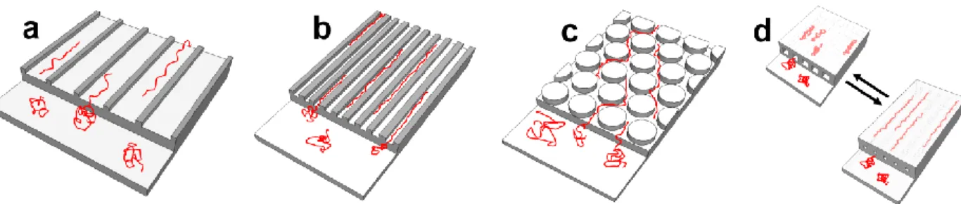
Figure 1.9 A depiction of nanofluidic device configurations used for DNA linearization by confinement.
These are (a) Nanoslit (b) Nanochannel (c) Nanopillar array, and (d) Tuneable-elastomeric based nanochannels
1.7.1.1 Optical Detection

![Figure 1.4 Illustration of differences in the electric potential and ionic concentrations for (A) Channels filled with moderately to highly concentrated electrolyte (and/or large channel height [h > λD]) and (B) Channels filled with low concentrated e](https://thumb-us.123doks.com/thumbv2/123dok_us/8323496.2206636/32.918.260.651.242.625/illustration-differences-potential-concentrations-moderately-concentrated-electrolyte-concentrated.webp)