International Airport Industrial Park • Mailing Address: PO Box 11400 • Tucson, AZ 85734 • Street Address: 6730 S. Tucson Blvd. • Tucson, AZ 85706 Tel: (520) 746-1111 • Twx: 910-952-1111 • Cable: BBRCORP • Telex: 066-6491 • FAX: (520) 889-1510 • Immediate Product Info: (800) 548-6132
High-Voltage, Internally Powered
ISOLATION AMPLIFIER
ISO107
FEATURES
● SIGNAL AND POWER IN ONE
TRIPLE-WIDE PACKAGE
● 8000Vpk TEST VOLTAGE
● 2500Vrms CONTINUOUS AC BARRIER
RATING
● WIDE INPUT SIGNAL RANGE:
–10V to +10V
● WIDE BANDWIDTH: 20kHz Small Signal, 20kHz Full Power
● BUILT-IN ISOLATED POWER:
±10V to ±18V Input, ±50mA Output
● MULTICHANNEL SYNCHRONIZATION
CAPABILITY (TTL)
DESCRIPTION
The ISO107 isolation amplifier provides both signal and power across an isolation barrier. The ceramic side-brazed hybrid package contains a transformer-coupled DC/DC converter and a capacitor-transformer-coupled signal channel.
Extra power is available on the isolated input side for external input conditioning circuitry. The converter is protected from shorts to ground with an internal cur-rent limit, and the soft-start feature limits the initial currents from the power source. Multiple-channel syn-chronization can be accomplished by applying a TTL clock signal to paralleled Sync pins. The Enable
con-trol is used to turn off transformer drive while keeping the signal channel demodulator active. This feature provides a convenient way to reduce quiescent current for low power applications.
The wide barrier pin spacing and internal insulation allow for the generous 2500Vrms continuous rating. Reliability is assured by 100% barrier breakdown testing that conforms to UL544 test methods. Low barrier capacitance minimizes AC leakage currents. These specifications and built-in features make the ISO107 easy to use, as well as providing for compact PC board layouts. Duty Cycle Modulator Oscillator Driver VOUT +VCC1 Enable –VCC2 –VCC1 Gnd 1 Com 1 VIN Sense +VCC2 Sync Gnd 2 Rectifiers Filters Com 2 Sync Duty Cycle Demodulator ISO107 BLOCK DIAGRAM
APPLICATIONS
● MULTICHANNEL ISOLATED DATA
ACQUISITION
● BIOMEDICAL INSTRUMENTATION
● POWER SUPPLY AND MOTOR CONTROL
● GROUND LOOP ELIMINATION
®
®
ISO107
2SPECIFICATIONS
ELECTRICALTA = +25°C and VCC2 = ±15V, ±15mA output current unless otherwise noted.
PARAMETERS CONDITIONS MIN TYP MAX UNITS ISOLATION
Rated Continuous Voltage (1)
AC, 60Hz TMIN to TMAX 2500 Vrms
DC TMIN to TMAX 3500 VDC
Test Breakdown, AC, 60Hz 10s 8000 Vpk
Isolation-Mode Rejection 2500Vrms, 60Hz 100 dB
2121VDC 160 dB
Barrier Impedance 1012 || 13 Ω || pF
Leakage Current 240Vrms, 60Hz 1.2 2 µA
GAIN
Nominal 1 V/V
Initial Error ±0.1 ±0.25 % FSR
Gain vs Temperature ±50 ±120 ppm/°C
Nonlinearity ±0.01 ±0.025 % FSR
INPUT OFFSET VOLTAGE
Initial Offset ±20 ±50 mV
vs Temperature ±150 ±400 µV/°C
vs Power Supplies VCC2 = ±10V to ±18V ±2 mV/V
INPUT
Voltage Range Output Voltage in Range ±10 ±15 V
Resistance 200 kΩ
SIGNAL OUTPUT
Voltage Range ±10 ±12.5 V
Current Drive ±5 ±15 mA
Ripple Voltage, 800kHz Carrier (See Figure 4) 20 mVp-p
Capacitive Load Drive 1000 pF
Voltage Noise 4 µV/√Hz
FREQUENCY RESPONSE
Small Signal Bandwidth 20 kHz
Slew Rate 1.5 V/µs
Settling Time 0.1%, –10/10V 75 µs
POWER SUPPLIES
Rated Voltage, VCC2 ±15 V
Voltage Range ±10 ±18 V
Input Current IO = ±15mA
(2) +75/–4.5 mA
Ripple Current No Filter 10 mAp-p
CIN = 1µF 3 mAp-p
Rated Output Voltage ±14.25 ±15 ±15.75 V
Output Current Balanced Load ±15 ±50 mA
Single 30 100 mA
Load Regulation Balanced Load 0.5 %/mA
Line Regulation 1.18 V/V
Output Voltage vs Temperature 10 mV/°C
Voltage Balance Error, ±VCC1 0.05 %
Voltage Ripple No External Capacitors 10 mVp-p
Output Capacitive Load (See Figure 1) 1 µF
Sync Frequency Sync-Pin Grounded(3) 1.6 MHz
TEMPERATURE RANGE
Specification –25 +85 °C
Operating –25 +85 °C
Storage –25 +125 °C
NOTES: (1) Conforms to UL544 test methods. 100% tested at 2500Vrms for 1 minute. (2) For other conditions, see Performance Curve, Input Current (+VCC2) vs Output Current. Input Current (–VCC2) is constant at –4.5mA (typ) for all output currents. (3) If using external synchronization with a TTL-level clock, frequency should be between
1.2MHz and 2MHz with a duty-cycle greater than 25%.
The information provided herein is believed to be reliable; however, BURR-BROWN assumes no responsibility for inaccuracies or omissions. BURR-BROWN assumes no responsibility for the use of this information, and all use of such information shall be entirely at the user’s own risk. Prices and specifications are subject to change without notice. No patent rights or licenses to any of the circuits described herein are implied or granted to any third party. BURR-BROWN does not authorize or warrant any BURR-BROWN product for use in life support devices and/or systems.
ABSOLUTE MAXIMUM RATINGS
Supply Without Damage ...±18V VIN, Sense Voltage ...±50V Com 1 to Gnd 1 or Com 2 to Gnd 2 ...±200mV Enable, Sync ... 0V to +VCC2 Continuous Isolation Voltage ... 2500Vrms VISO, dv/dt ... 20kV/µs Junction Temperature ... 150°C Storage Temperature ... –25°C to +125°C Lead Temperature, (soldering, 10s) ... 300°C Output Short to Gnd 2 Duration ... Continuous ±VCC1 to Gnd 1 Duration ... Continuous
PIN CONFIGURATION
PACKAGE INFORMATION(1)
PACKAGE DRAWING MODEL PACKAGE NUMBER
ISO107 32-Pin Side-Braze Ceramic 210
NOTE: (1) For detailed drawing and dimension table, please see end of data sheet, or Appendix D of Burr-Brown IC Data Book.
Top View DIP
1 2 3 4 32 31 30 29 20 19 18 17 13 14 15 16 NC +V NC –V CC1 CC1 Com 2 V Sense Gnd 2 OUT NC Gnd 1 V Com 1 IN –V Sync* +V Enable CC2 CC2
*Operation requires that this pin be grounded or driven with TTL levels.
ELECTROSTATIC
DISCHARGE SENSITIVITY
Any integrated circuit can be damaged by ESD. Burr-Brown recommends that all integrated circuits be handled with ap-propriate precautions. Failure to observe proper handling and installation procedures can cause damage.
ESD damage can range from subtle performance degradation to complete device failure. Precision integrated circuits may be more susceptible to damage because very small parametric changes could cause the device not to meet published speci-fications.
®
ISO107
4TYPICAL PERFORMANCE CURVES
TA = +25°C, VCC2 = ±15VDC, ±15mA output current unless otherwise noted.RECOMMENDED RANGE OF ISOLATION VOLTAGE 10k
10 100 1k 10k 100k
Maximum Isolation Voltage (Vpk)
Isolation Voltage Frequency (Hz) 3.5k 1k 100 10 1 1M Operational Region
Barrier Voltage Rating
Non-Specified Signal Operation
PSRR vs FREQUENCY
Supply Modulation Frequency (Hz)
100 1k 10k 100k 60 54 40 20 0
Power Supply Rejection Ratio (dB)
–VCC2 +VCC2 20 10 0 –10 –20 Output Voltage (V) Time (µs) 0 50 100
LARGE SIGNAL TRANSIENT RESPONSE
IMR/LEAKAGE vs FREQUENCY 120 100 80 60 40 20 10 100 1k 10k 100k Isolation-Mode Rejection (dB) 10mA 1mA 100µA 10µA 1µA 100nA
Barrier Leakage Current (rms)
Isolation Voltage Frequency (Hz)
Leakage at 240 Vrms Leakage at 2500 Vrms IMR GAIN/PHASE vs FREQUENCY 3 0 –3 –6 –9 –12 –15 –45 0 45 90 135 180 225 300 1k 3k 30k 100k
Small Signal Frequency (Hz)
Gain (dB) Phase Shift (°)
100 10k
Gain
Phase
ISOLATED POWER SUPPLY LOAD REGULATION AND EFFICIENCY 18 16 14 12 10 60 45 30 15 0 10 20 30 40 50 20 40 60 80 100
±V Supply Output Current (mA)CC1
±V Output Voltage (V)
CC1
Balanced Load Efficiency
Output Voltage Balanced Loads Output Voltage Single-Ended Loads Efficiency (%) 0 0
TYPICAL PERFORMANCE CURVES
(CONT) TA = +25°C, VCC2 = ±15VDC, ±15mA output current unless otherwise noted.ISOLATED POWER SUPPLY LINE REGULATION
+V (V)CC2 ±V (V) CC1 19 18 17 16 15 14 13 12 11 10 9 ±15mA Load 1.18 V/V 9 10 11 12 13 14 15 16 17 18 19
ISOLATED POWER SUPPLY VOLTAGE vs TEMPERATURE Temperature (°C) 2 1 0 –1 –2 –25 0 25 50 75 100 V (%)CC1 ∆
ISOLATED SUPPLY VOLTAGE AND V vs SYNC FREQUENCY Sync Frequency (MHz) 5 2.5 0 –2.5 –5 1 1.5 2 2.5 V (mV)OS∆ OS V (mV)CC1∆ 50 25 0 –25 –50 VCC1 VOS
+VCC1 Supply Balanced Output Current (mA) +VCC2 = 15V
ISOLATED POWER SUPPLY INPUT CURRENT vs OUTPUT CURRENT 145 120 95 70 ±V CC2
Input Current (mA)
0 45
®
ISO107
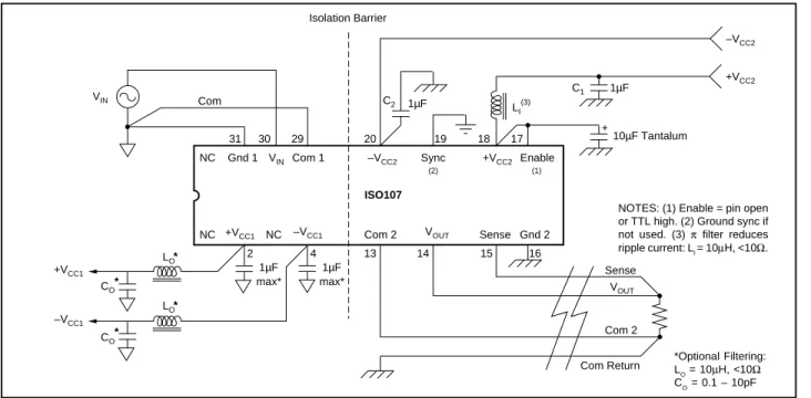
6NOTES: (1) Enable = pin open or TTL high. (2) Ground sync if not used. (3) π filter reduces ripple current: LI = 10µH, <10Ω.
THEORY OF OPERATION
The block diagram on the front page shows the isolation amplifier’s synchronized signal and power configuration, which eliminates beat frequency interference. A proprietary 800kHz oscillator chip, power MOSFET transformer driv-ers, patented square core wirebonded transformer, and single chip diode bridge provide power to the input side of the isolation amplifier as well as external loads. The signal channel capacitively couples a duty-cycle encoded signal across the ceramic high-voltage barrier built into the pack-age. A proprietary transmitter-receiver pair of integrated circuits, laser trimmed at wafer level, and coupled through a pair of matched “fringe” capacitors, result in a simple, reliable design.
SIGNAL AND POWER CONNECTIONS
Figure 1 shows the proper power supply and signal connec-tions. All power supply pins should be bypassed as shown with the π filter for +VCC2 an option recommended if more than ±15mA are drawn from the isolated supply. The sepa-rate input and output common pins and output sense are low current inputs tied to the signal source ground, output ground, and output load, respectively, to minimize errors due to IR drop in long conductors. Otherwise, connect Com 1 to Gnd 1, Com 2 to Gnd 2, and Sense to VOUT at the ISO107 socket. The enable pin may be left open if the ISO107 is continuously operated. If not, a TTL low level will disable the internal DC/DC converter. The Sync input must be grounded for unsynchronized operation while a 1.2MHz to 2MHz TTL clock signal provides synchronization of mul-tiple units.
OPTIONAL GAIN AND OFFSET ADJUSTMENTS
Rated gain accuracy and offset performance can be achieved with no external adjustments, but the circuit of Figure 2a may be used to provide a gain trim of ±0.5% for the values shown; greater range may be provided by increasing the size of R1 and R1. Every 2kΩ increase in R1 will give an additional 1% adjustment range, with R2 ≥ R1. If safety or convenience dictates location of the adjustment potentiome-ter on the other side of the barrier from the position shown in Figure 2a, the position of R1 and R2 may be reserved. Gains greater than 1 may be obtained by using the circuit of Figure 2b. Note that the effect of input offset errors will be multiplied at the output in proportion to the increase in gain. Also, the small-signal bandwidth will be decreased in
in-FIGURE 1. Signal and Power Connections.
FIGURE 2b. Gain Setting. VIN 30 29 15 14 13 VOUT Sense R1 R2 Gain = 1 + +R1 R1 R2 200k
( )
FIGURE 2a. Gain Adjust.1kΩ VIN R1 30 29 2kΩ R2 15 14 13 VOUT *Optional Filtering: LO = 10µH, <10Ω CO = 0.1 – 10pF NC Gnd 1 –VCC2 Sync 31 30 29 20 19 18 17 Enable +VCC2 (2) (1) 1µF L I (3) 1µF 10µF Tantalum + 16 15 14 13 Sense Com 2 Com Return VOUT –VCC1 +VCC1 VIN Com 1 NC +VCC1 NC –VCC1 ISO107 * * CO CO * * LO LO VIN Com Isolation Barrier 4 2 1µF max* +VCC2 –VCC2
Com 2 VOUT Sense Gnd 2 1µF
max*
C1 C2
verse proportion to the increase in gain. In most instances, a precision gain block at the input of the isolation amplifier will provide better overall performance.
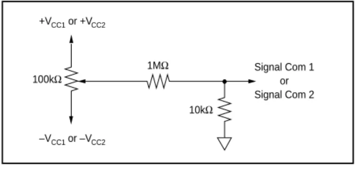
Figure 3 shows a method for trimming VOS of the ISO107. This circuit may be applied to either Signal Com (input or output) as desired for safety or convenience. With the values shown, ±15V supplies and unity gain, the circuit will pro-vide ±150mV adjustment range and 0.25mV resolution with a typical trim potentiometer. The output will have some sensitivity to power supply variations. For a ±100mV trim, power supply sensitivity is 8mV/V at the output.
ISOLATION BARRIER VOLTAGE
The typical performance of the ISO107 under conditions of barrier voltage stress is indicated in the first two perform-ance curves—Recommended Range of Isolation Voltage and IMR/Leakage vs Frequency. At low barrier modulation levels, errors can be determined by the IMRR characteristic. At higher barrier voltages, typical performance is obtained as long as the dv/dt across the barrier is below the shaded area in the first curve. Otherwise, the signal channel will be interrupted, causing the output to distort, and/or shift DC level. This condition is temporary, with normal operation resuming as soon as the transient subsides. Permanent dam-age to the integrated circuits occurs only if transients exceed 20kV/µs. Even in this extreme case, the barrier integrity is assured.
HIGH VOLTAGE TESTING
The ISO107 was designed to reliably operate with 2500Vrms continuous isolation barrier voltage. To confirm barrier integrity, a two-step breakdown test is performed on 100% of the units. First, an 8000V peak, 60Hz barrier potential is applied for 10s to verify that the dielectric strength of the insulation is above this level. Following this exposure, a 2500Vrms, 60Hz potential is applied for one minute to conform to UL544. Life-test results show reliable operation under continuous rated voltage and maximum operating temperature conditions.
OPTIONAL OUTPUT FILTER
Figure 4 shows an optional output ripple filter that reduces the 800kHz ripple voltage to <3mVp-p without compromis-ing DC performance. The small signal bandwidth is ex-tended above 30kHz as a result of this compensation. FIGURE 3. VOS Adjust. +V or +VCC1 CC2 100kΩ 10kΩ 1MΩ Signal Com 1 or Signal Com 2 –V or –VCC1 CC2 MULTICHANNEL SYNCHRONIZATION
Synchronization of multiple ISO107s can be accomplished by connecting pin 19 of each device to an external TTL level oscillator, as shown in Figure 6. The PWS750-1 oscillator is convenient because its nominal synchronizing output fre-quency is 1.6MHz, resulting in a 800kHz carrier in the ISO107 (its nominal unsynchronized value). The open col-lector output typically switches 7.5mA to a 0.2V low level so that the external pull-up resistor can be chosen for different pull-up voltages as shown in Figure 6. The number of channels synchronized by one PWS750-1 is determined by the total capacitance of the sync voltage conductors. They must be less than 1000pF to ensure TTL level switching at 800kHz. At higher frequencies the capacitance must be proportionally lower.
Customers can supply their own TTL level synchronization logic, provided the frequency is between 1.2MHz and 2MHz, and the duty cycle is greater than 25%.
FIGURE 4. Ripple Reduction. VIN 30 29 15 14 13 VOUT Sense 400 4.7nF Ω
®
ISO107
8 18 – + – + IC2B +15V 14 15 19 16 13 2kΩ R12 R13 10kΩ R14 10kΩ VOUT –15V 20 4 2 30 31 29 C4 0.1µF R11 10kΩ Q3 R7 10M C3 0.33µF R8 2kΩ R9 100kΩ 6 5 7 R10 100kΩ 9 10 6 + 8 – 7 R4 R5 R6 10kΩ C1 2.2nF R1 330kΩ R2 330kΩ RA LA Q1 Q2 + 8 4 – – + 2 3 IC2A RL R3 330kΩ Q4 – + 1 11, 12 16 3 2 C2 10nF IC1 INA110* IC3 ISO107* Ω D1 IC2 OPA2111* Q1, Q2, Q4 2N3904 Q3 2N7000 D1 IN4148 R1, R2, R3 1%, 1/2W R4, R5 1%, 2210Ω IC1, IC3 Bypass 1.0µF IC2 Bypass 0.1µF *Burr-Brown P/NFIGURE 5. ECG Amplifier with Right Leg Drive, Defibrillator Protection, and E.S.U. Blanking.
FIGURE 6. Synchronized-Multichannel Isolation.
NOTES: (1) PWS750-1 can sync >20 ISO107s. (2) Bypass supplies as shown in Figure 1. +VCC2 –VCC2 VIN1 Channel 1 ISO 107 2 31 30 29 20 19 18 Sync 1.6MHz PWS750-1 12 14 11 4 13 14 15 16 R 3 7 VIN2 + – 31 30 29 20 19 18 2 4 13 14 15 16 VOUT1 VOUT2 ISO 107 Additional Channels Channel 2 + – ≈
APPLICATIONS
PACKAGING INFORMATION
Orderable Device Status(1) Package Type
Package Drawing
Pins Package Qty
Eco Plan(2) Lead/Ball Finish MSL Peak Temp(3) ISO107 NRND CDIP SB JVF 16 TBD Call TI Call TI
(1)
The marketing status values are defined as follows: ACTIVE: Product device recommended for new designs.
LIFEBUY: TI has announced that the device will be discontinued, and a lifetime-buy period is in effect.
NRND: Not recommended for new designs. Device is in production to support existing customers, but TI does not recommend using this part in a new design.
PREVIEW: Device has been announced but is not in production. Samples may or may not be available. OBSOLETE: TI has discontinued the production of the device.
(2)Eco Plan - The planned eco-friendly classification: Pb-Free (RoHS), Pb-Free (RoHS Exempt), or Green (RoHS & no Sb/Br) - please check
http://www.ti.com/productcontentfor the latest availability information and additional product content details. TBD: The Pb-Free/Green conversion plan has not been defined.
Pb-Free (RoHS): TI's terms "Lead-Free" or "Pb-Free" mean semiconductor products that are compatible with the current RoHS requirements for all 6 substances, including the requirement that lead not exceed 0.1% by weight in homogeneous materials. Where designed to be soldered at high temperatures, TI Pb-Free products are suitable for use in specified lead-free processes.
Pb-Free (RoHS Exempt): This component has a RoHS exemption for either 1) lead-based flip-chip solder bumps used between the die and package, or 2) lead-based die adhesive used between the die and leadframe. The component is otherwise considered Pb-Free (RoHS compatible) as defined above.
Green (RoHS & no Sb/Br): TI defines "Green" to mean Pb-Free (RoHS compatible), and free of Bromine (Br) and Antimony (Sb) based flame retardants (Br or Sb do not exceed 0.1% by weight in homogeneous material)
(3) MSL, Peak Temp. -- The Moisture Sensitivity Level rating according to the JEDEC industry standard classifications, and peak solder
temperature.
Important Information and Disclaimer:The information provided on this page represents TI's knowledge and belief as of the date that it is provided. TI bases its knowledge and belief on information provided by third parties, and makes no representation or warranty as to the accuracy of such information. Efforts are underway to better integrate information from third parties. TI has taken and continues to take reasonable steps to provide representative and accurate information but may not have conducted destructive testing or chemical analysis on incoming materials and chemicals. TI and TI suppliers consider certain information to be proprietary, and thus CAS numbers and other limited information may not be available for release.
In no event shall TI's liability arising out of such information exceed the total purchase price of the TI part(s) at issue in this document sold by TI to Customer on an annual basis.
PACKAGE OPTION ADDENDUM
www.ti.com 2-Feb-2009
IMPORTANT NOTICE
Texas Instruments Incorporated and its subsidiaries (TI) reserve the right to make corrections, modifications, enhancements, improvements, and other changes to its products and services at any time and to discontinue any product or service without notice. Customers should obtain the latest relevant information before placing orders and should verify that such information is current and complete. All products are sold subject to TI’s terms and conditions of sale supplied at the time of order acknowledgment.
TI warrants performance of its hardware products to the specifications applicable at the time of sale in accordance with TI’s standard warranty. Testing and other quality control techniques are used to the extent TI deems necessary to support this warranty. Except where mandated by government requirements, testing of all parameters of each product is not necessarily performed.
TI assumes no liability for applications assistance or customer product design. Customers are responsible for their products and applications using TI components. To minimize the risks associated with customer products and applications, customers should provide adequate design and operating safeguards.
TI does not warrant or represent that any license, either express or implied, is granted under any TI patent right, copyright, mask work right, or other TI intellectual property right relating to any combination, machine, or process in which TI products or services are used. Information published by TI regarding third-party products or services does not constitute a license from TI to use such products or services or a warranty or endorsement thereof. Use of such information may require a license from a third party under the patents or other intellectual property of the third party, or a license from TI under the patents or other intellectual property of TI.
Reproduction of TI information in TI data books or data sheets is permissible only if reproduction is without alteration and is accompanied by all associated warranties, conditions, limitations, and notices. Reproduction of this information with alteration is an unfair and deceptive business practice. TI is not responsible or liable for such altered documentation. Information of third parties may be subject to additional restrictions.
Resale of TI products or services with statements different from or beyond the parameters stated by TI for that product or service voids all express and any implied warranties for the associated TI product or service and is an unfair and deceptive business practice. TI is not responsible or liable for any such statements.
TI products are not authorized for use in safety-critical applications (such as life support) where a failure of the TI product would reasonably be expected to cause severe personal injury or death, unless officers of the parties have executed an agreement specifically governing such use. Buyers represent that they have all necessary expertise in the safety and regulatory ramifications of their applications, and acknowledge and agree that they are solely responsible for all legal, regulatory and safety-related requirements concerning their products and any use of TI products in such safety-critical applications, notwithstanding any applications-related information or support that may be provided by TI. Further, Buyers must fully indemnify TI and its representatives against any damages arising out of the use of TI products in such safety-critical applications.
TI products are neither designed nor intended for use in military/aerospace applications or environments unless the TI products are specifically designated by TI as military-grade or "enhanced plastic." Only products designated by TI as military-grade meet military specifications. Buyers acknowledge and agree that any such use of TI products which TI has not designated as military-grade is solely at the Buyer's risk, and that they are solely responsible for compliance with all legal and regulatory requirements in connection with such use. TI products are neither designed nor intended for use in automotive applications or environments unless the specific TI products are designated by TI as compliant with ISO/TS 16949 requirements. Buyers acknowledge and agree that, if they use any non-designated products in automotive applications, TI will not be responsible for any failure to meet such requirements.
Following are URLs where you can obtain information on other Texas Instruments products and application solutions:
Products Applications
Amplifiers amplifier.ti.com Audio www.ti.com/audio
Data Converters dataconverter.ti.com Automotive www.ti.com/automotive
DLP® Products www.dlp.com Broadband www.ti.com/broadband
DSP dsp.ti.com Digital Control www.ti.com/digitalcontrol
Clocks and Timers www.ti.com/clocks Medical www.ti.com/medical
Interface interface.ti.com Military www.ti.com/military
Logic logic.ti.com Optical Networking www.ti.com/opticalnetwork
Power Mgmt power.ti.com Security www.ti.com/security
Microcontrollers microcontroller.ti.com Telephony www.ti.com/telephony
RFID www.ti-rfid.com Video & Imaging www.ti.com/video
RF/IF and ZigBee® Solutions www.ti.com/lprf Wireless www.ti.com/wireless
Mailing Address: Texas Instruments, Post Office Box 655303, Dallas, Texas 75265 Copyright © 2009, Texas Instruments Incorporated