Compact low-noise RF resonator for
cryogenic trapped ion quantum
computer
By
Margie Bruff
Senior Honors Thesis
Department of Physics and Astronomy University of North Carolina at Chapel Hill
May 1st, 2020
Approved:
Dr. Julieta Gruszko, Thesis Advisor
Dr. Lu-Chang Qin, Reader
Contents
1 Introduction 1
2 Design 3
2.1 RLC resonator . . . 3
2.2 Coil design . . . 4
2.3 Impedance matching . . . 5
2.4 Implementation . . . 7
2.5 Simulations . . . 9
3 Experimental Testing 10 3.1 Reflectance . . . 10
3.2 High voltage . . . 15
4 Results and Analysis 15 4.1 Room temperature . . . 15
4.2 Low temperature . . . 16
Acknowledgments
This work was done at the MIST lab at Duke University under the advisorship of Prof. Jungsang Kim and Dr. Stephen Craine and in collaboration with Ke Sun. Prof.
Abstract
The Duke Multifunctional Integrated Systems Technology (MIST) lab uses trapped Yb+ ions for quantum information processing. Trapped ions are promising qubits due to their long coherence time and ease of manipulation. However, ion trapping requires high voltage radio frequency (RF) signals, on the order of hundreds of volts for heavy ions like Yb+. The state-of-the-art mechanical resonator used to achieve these voltages is bulky and noisy, disrupting motional coherence between the ions and lasers used to control them. We study an alternative electronic component resonator. We aimed to maximize voltage gain, Gv, without exceeding a quality factor,Q, threshold of 200, to
keep the RF voltage stable to small changes in frequency. We designed three inductor coils with sequential improvements to increase thermal conductivity and decrease internal resistance. We tested these coils using a capacitor as a model of the ion trap and foundGv ≈40 for the first two coils with Q <200 for ideally impedance matched
1 Introduction
Coherent control of atomic ions has long been of interest in atomic physics for precision measurement and other studies of fundamental physics. More recently, trapped ions have become a key player on the quantum information stage. Quantum information involves the use of a system with discrete states, taking advantage of the principles of quantum mechanics for computing, communication, cryptography, and further study of quantum phenomena. In a computing framework, the system is composed of qubits, or quantum bits, which can be in the state|0>,|1>, or any superposition of|0>, and |1>, and can become entangled with other qubits. As predicted by quantum mechanics, the measurement or readout of qubits results in the collapse of their state onto the measurement basis. These properties allow qubits to speed up certain algorithms, provide secure channels for cryptography, and speed up communication.
Though any two level quantum system can provide the physical implementation of a qubit, ideal systems from which to create a universal quantum computer must satisfy DiVincenzo’s requirements: (1) they can be initialized into a certain state, (2) they can be manipulated between states with a set of universal gates, (3) they have coherence time much longer than gate operation time, (4) they can be measured and the two levels distinguished on a qubit by qubit basis, and (5) they can be scaled up to
thousands (quantum emulation) or even millions (quantum computing) of qubits in the same system [1]. Though no system has achieved all five criteria, trapped ions are one of the most promising current implementations.
To achieve coherent control over the ions, they are trapped using electric fields. By Gauss’ law it is not possible to create a central electric potential with no charge enclosed. That is, where E* is the electric field and U is the potential,
∇ ·E*= 0 =⇒ ∇ ·(−∇U) = −∇2U = 0. (1.1)
This means that a static field alone cannot generate the potential well to trap ions.
Instead, a traditional Paul trap uses four quadrupolar electrodes with diagonal pairs corresponding to the same voltage [2]. One pair is grounded and the other has an AC voltage applied (Figure 1a). This creates a saddle point electric potential with polarity changing fast enough to confine ions along the axis parallel to the electrodes (Figure 1b). The equations of motion for ions in such a potential are solved by a set of solutions known as Mathieu’s equations [3]. According to these solutions, ions are stable in
specific regions of voltage-frequency parameter space [4].
One common operating point, which is used in the MIST lab, is radio frequencies (RF) and voltages of tens to hundreds of volts. While a voltage of tens of volts is
Figure 1: A schematic of the traditional 4-electrode Paul trap (a) side-view and (b) end view, (c) surface Paul trap and electric potential mapping, and (d) implemented surface trap image [8]
such as Yb+ confined. Yb+ is of particular interest in the MIST lab due to its simple energy level structure and the ability to address the relevant energy transitions with commercial lasers. [3, 6].
Working toward an implemented design for computing, the traditional Paul trap was modified into a surface Paul trap by folding the electrodes out onto an insulating surface (Figure 1c; [7] et al, 2006). The potential well extends in the same direction, parallel to the length of the electrodes, but now the potential null sits 50−200µm
above the surface (Figure 1d, [8]).
Trapped ions are most limited as qubits by poor scalability [9, 10]. Chains of ions can be confined in the same trap, but interactions with background gas make long chains less likely to stay confined. To reduce these interactions, the system can be placed in a cryostat. The improved vacuum makes interactions less common and low temperatures significantly reduce the energy of any collisions that do occur, so they are less likely to disrupt the ion chain. However, a cryostat presents new limitations including low input power limits (of order mW) and the inability to use active circuit components. A cryogenic ion trap then greatly improves the system for applications to quantum computing and simulation but requires a high-gain passive component resonator.
Figure 2: The state of the art resonator used to achieve high trapping voltages is a helical resonator which relies on a mechanical design that is susceptible to vibrations [11]
(Figure 2). This is highly susceptible to mechanical vibrations which can introduce variability to the RF voltage amplitude and change the motional frequency of ions. This is known as phase noise or phase decoherence since it leads to loss of coherence with the lasers used to control the ions. The helical resonator provides voltage gain,
Gv ≈60, for trap voltages 200V < Vt<300V. The goal of this project is to design a
compact high-gain passive electronic component resonator for use on Yb+ systems that will achieve comparable voltage gain in this voltage operating range but introduce less phase noise.
2 Design
2.1 RLC resonator
A resistor, inductor, and capacitor (RLC) in series form a high-gain resonator and can achieve high voltages with low input power. The magnitude of total impedance in an ideal series RLC circuit is given by,
Z =pR2 + (X
L−XC)2, (2.1)
where R is the resistance, XL =ωL is the inductive reactance (with ω being the
frequency andL the inductance), and XC = ωC1 is the capacitive reactance (with C
being the capacitance). Resonance occurs when the impedance is entirely real and resistive, that is, when Z =R, and XL =XC. The resonance frequency, then, is given
byω0 = √LC1 in rad/s or f0 = 2π√1LC in Hz. To achieve a target f0 = 55 MHz with the
ion trap itself acting as a 10pF capacitor, we aim for L= 0.837µH.
In an ideal series RLC circuit, the current is constant throughout and given by Ohm’s law as I = Vin
voltage divider, the expected voltage gain measured over the capacitor is given by,
Vc
Vin
= Xc
Z . (2.2)
At resonance in an ideal RLC resonator, this provides a maximum voltage gain,
Gv =
1
R
r
L
C. (2.3)
In our resonator with C fixed as the trap capacitance and L fixed as above to set the desired resonance frequency, to maximize voltage gain we need to minimize the resistance in our coil design.
2.2 Coil design
Inductance is based entirely on the geometry of a coil and is given by L= NIΦ, where
N is the number of turns, Φ is the magnetic flux through the area of wire, andI is the current through the wire. For a rectangular cross-sectional toroidal coil, the magnetic field,
B = µ0N I
2πR . (2.4)
Then, Φ = µ0hM
2π ln( r2
r1)I ,where his the height of the coil, r1 is the radial distance to the
inner edge, and r2 is the radial distance to the outer edge. The inductance for this
particular geometry, then, is given by
L= µ0hN
2
2π ln r2
r1
. (2.5)
In particular, the inductance of a square cross-sectional toroid, in contrast to that of a circular cross-sectional toroid, does not depend on either radius individually, but only on the ratio between the two. Using this geometry will provide more freedom to make the coil compact and have less resistance. However, we need to have enough turns to produce a uniform field and we are limited by the drilling resolution and structural integrity of the insulating piece supporting the wires, which is made of TeflonR in this
case.
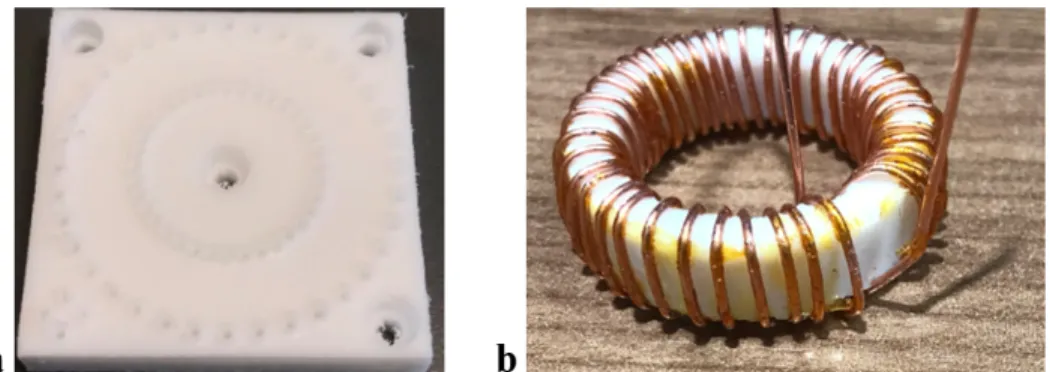
Figure 3: a) Teflon guide piece for 1st and 2nd generation design; (b) Teflon guide piece with completed coil for 3rd generation design
Coil N h (mm) r1 (mm) r2 (mm) R(Ω) L(µH)
1st gen 23 6.8 13.82 16.17 0.300 0.902 2nd gen 23 6.8 13.82 16.17 0.288 0.872 3rd gen 40 6.8 5.10 7.68 0.137 0.833
Table 1: Design parameters and measured resistance and inductance for each coil. The design parameters were optimized to achieveL ≈ 0.837µH while minimizing the size of the coil (based on Equation 2.5). The resistances were measured directly using a digital multimeter and the inductances were measured
indirectly by finding resonance with a test capacitor using a spectrum analyzer.
While Teflon has a good combination of the required material properties, its thermal conductivity is not as high as would be ideal. With the 2nd generation coil, we used Nb3Sn+Copper wire, which is superconducting below 12K but acts as a normal copper wire at higher temperatures, so that the inductor would not heat as quickly. In a third design iteration (3rd generation, Figure 3b) we used a similar superconducting wire (NbTi), but we aimed to minimize the quantity of Teflon, and included just enough, in the form of the toroid core only, to attach the coil to the coldfinger. This enabled us to make the design even smaller, since, with cryogenic varnish to insulate and stabilize them, each turn could be directly adjacent to the next instead of following holes in the guide piece. The design properties, resistance (measured directly), and inductance (measured from resonance frequency with test capacitor) of each coil generation are given in Table 1.
2.3 Impedance matching
To achieve a target voltage gain upwards of Gv ≈60, we need the resistance of the
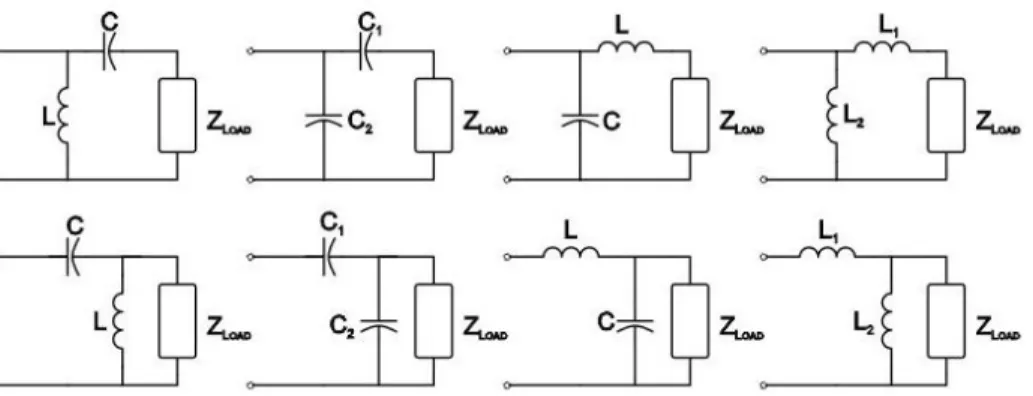
Figure 4: Possible L-network impedance matching configurations to reduce signal reflection. The low resistance of the resonator (denotedZload) compared to
the source can only be matched using designs on the top row. Given the measured coil resistances, the third design is most favorable, with a linear dependence on the matching inductance and a quadratic dependence on the matching capacitance. The required matching inductance is on the order of tens of nH and the required matching capacitance is on the order of hundreds of pF
reflection coefficient describes the ratio of the reflected voltage to the input voltage and is given by
Γ = Vr
Vin
= ZL−ZS
ZL+ZS
, (2.6)
where ZS is the source impedance, which is entirely real (resistive) and equal to 50Ω,
and ZL is the load impedance. At resonance, XC =XL, so ZL=R. Almost all the
power is reflected back onto the source instead of reaching the trap. The efficiency of the design, that is, the ratio of output power to input power, then is given by
ξ = Pout
Pin
= 1−Γ2. (2.7)
For all three coil designs, Γ≈0.99 without impedance matching. This corresponds to an efficiency below 2%. SinceP ∝V2, this high reflection coefficient will result in less
than 15% of the voltage gain being realized.
We can use additional reactive circuit elements to match the impedances and prevent reflection without increasing the effective resistance, and thereby without decreasing
Gv. The smallest number of reactive elements we would need is two: one in either series
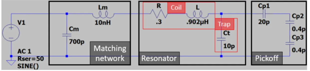
Figure 5: Annotated schematic of full implementation circuit. The chosen L-network provides impedance matching of the voltage input onto the resonator, which consists of the coil and trap, and the signal is detected with a capacitive pickup network
A network with elements in parallel to the resonator and series with the source will only provide perfect matching in the case whereZL> ZS. SinceR 50Ω, this rules
out the bottom row of networks in Figure 4. Solving for the total impedance of the third network in the top row, we found that it depended linearly on the matching inductance,Lm, with an optimal value on the order of 10 nH, and depended
quadratically on the matching capacitance, Cm, with ideal value on the order of
hundreds of pF. This unique coincidence allows us to use the trace inductance from the PCB, which is on the order of nH but is otherwise unknown, in addition to just a single capacitance value, to provide nearly-perfect impedance matching.
2.4 Implementation
Altogether, the circuit (shown in Figure 5) consists of the resonator (with resistance
R, coil inductance L, and trap capacitanceCt), the matching network (with matching
inductance Lm and matching capacitance Cm), and a pickoff network to measure the
voltage across the trap. The pickoff network consists of a 20pF capacitor in series with a 0.2pF capacitor, together in parallel with the trap. These components divide the magnitude of the voltage across the trap so that roughly 1% is across the 20pF capacitor. The voltage is measured in real time over the 20pF capacitor. The 0.2pF capacitor is implemented as two 0.4pF capacitors in series in order to not exceed the voltage limits of an individual capacitor.
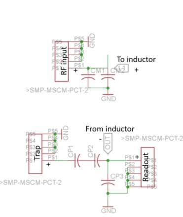
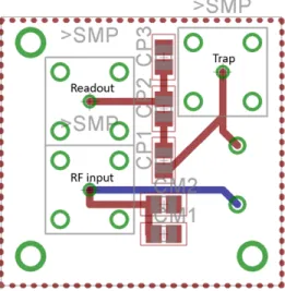
We implemented the design using a printed circuit board (PCB). We used the Autodesk Easily Applicable Graphical Layout Editor (EAGLE) software to design the PCB. Figure 6 shows how we created the board schematic using SMP connectors for input and output signals including the RF input, connection to the trap, and pickoff readout. We implemented the single capacitance value as two capacitors (shown
schematically as Cm in Figure 5) in parallel to enable the use of combinations for more
grounding on the top. We added two ungrounded vias at the L1 and OUT nodes for the connections to the coil and added three grounded vias at open corners for screws to secure the board inside the cryostat.
Figure 7: Annotated EAGLE board diagram. Red lines denote traces on the top layer and blue lines denote traces on the bottom layer. The red border denotes extra grounding on the bottom layer. Green circles denote vias: four grounded and one signal via on each SMP connector and three grounded vias for mechanical connections to the coldfinger.
2.5 Simulations
We used Mathematica to analytically add impedances of sequential circuit
components in the complete schematic (Figure 5) to find the total output impedance and produce a model forGv = VVc
in (as in Equation 2.2), whereVc is now the voltage
across the trap, Vt. This is akin to the derivation in Section 2.1, but with additional
components making the gain function more complicated. We then used this model to simulate the circuit and find the expectedCm for a range of R (Figure 8). We
estimated the coil inductance to be 0.85µH, the capacitance of the trap to be 10pF, and the inductance of the trace between the matching capacitor and resonator, Ltrace, to be
10nH. We simulated the circuit voltage response with a range of matching capacitance values for different values of resonator resistance. The resonator resistance is expected to be the measured coil resistance at room temperature (Section 2.2), but to decrease at lower temperature. We find that the ideal matching capacitance is larger for smaller resistances, ranging from 937.2pF at R = 0.1Ω to 382.8pF at R = 1.1Ω. We also find that the magnitude of voltage gain is about twice as high for R = 0.1Ω as compared to
Figure 8: Simulation output of voltage gain as a function of matching capacitance for different coil resistances. We find the best expected matching (denoted by the dashed vertical line) to be higher for lower resistance coils. We also find an expected factor of two improvement in voltage gain for this one order of magnitude drop in resistance.
3 Experimental Testing
3.1 Reflectance
We evaluated the performance of the resonator experimentally by first characterizing the reflected signal with a range of test matching capacitances. For these tests, we soldered a capacitor on the PCB in place of an SMP connector to the trap in order to emulate the trap. We expect the signal to be entirely reflected except around the resonance frequency, hereinafter f, where we expect a dip in the reflection. The depth,
d, of the dip should be larger for a more ideally matched circuit.
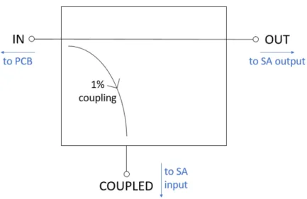
We used an Agilent spectrum analyzer and a directional coupler to measure the frequency response of the reflected signal. The spectrum analyzer output a −10 dBm signal which we directed through the reverse coupler main line (as shown in Figure 9) with minimal (<1dB) loss. This served as the PCB input signal. The reflected signal from the PCB then traversed the main line and 1% was picked up through the coupled output, which we measured with the spectrum analyzer. We expect the baseline, when all of the signal is reflected and no additional input is present, to be at 1% of −10dBm, or−30dBm.
We conducted an automatic frequency sweep of the spectrum analyzer output over a range of relevant frequencies (roughly 35−60MHz). We analyzed the frequency
Figure 9: Directional coupler assembly schematic for reflection measurements. 1% of the reflected signal from the resonator PCB load (IN) is coupled and measured on the spectrum analyzer
fell below the baseline by more than the loss threshold (1dB). The minimum of this dip isf, the resonance frequency. We found the quality factor, Q, from the ratio of the resonance frequency to bandwidth, ∆f, where the bandwidth is the frequency range between the right and left half-power points, fR and fL, respectively, of the transmitted
signal, that is,
Q= f ∆f =
f fR−fL
(3.1)
Since the reflected and transmitted signal must add to the total input signal, the baseline power of the reflected signal is equal to the peak power of the transmitted signal. Thus, we used the two points where the signal crossed 3dB below the baseline power, for which there was always one to the left and one to the right of the resonance frequency as fR and fL, respectively. If Q is too large then it will not be feasible to
maintain steady RF voltage since small changes in frequency will result in large changes in voltage. We aim to not exceed Q= 200.
We found the depth, d, by subtracting the minimum power at the center of the dip from the baseline power. We comparedd for a range of matching capacitance values and identified the one with highest d as most ideally impedance matched. We are limited in the scale of this test by the increments of capacitance values that are
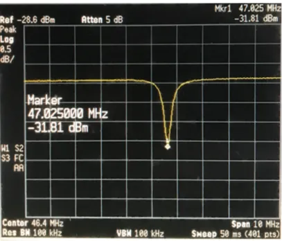
Figure 10: Example spectrum analyzer output from frequency sweep reflection measurement. This early measurement shows a resonance frequency of 47.025 MHz and depth of only 3.2 dB (below the −28.6 dBm baseline)
We first performed this test at room temperature, using a 10pF capacitor to emulate the trap, to determine if the resonator behaved as predicted by simulations, if our matching network was feasible, if we could select a matching capacitance without limiting the gain, and whether Q stayed below 200.
We also performed this test at low temperature in a closed-cycle Helium recirculation vacuum cryostat with minimum temperature of 5K (Figure 11). In these low
temperature experiments we aimed to determine the matching capacitance, since it would differ from that at room temperature due to changes in impedance, especially resistance, and to find the change inQ. At low temperature, we used a 17pF capacitor due to temperature limitations on the 10pF capacitor.
We record the spectrum analyzer curve at equally spaced intervals during the total 10 hour cryostat cool down process (Figure 12). We compare f0,d, andQ at the final,
Figure 11: 3rd generation coil and PCB on the cryostat coldfinger assembly
Figure 12: Spectrum analyzer reflection curves at equally spaced time intervals during cool down of the 2nd generation coil with Cm = 485pF. The color gradient
Figure 13: Characteristics of reflection curve as a function of time during cool down of the 2nd generation coil with Cm = 485pF. The circuit is very well matched
3.2 High voltage
In order to evaluate the voltage gain of the resonator, and determine whether we have achieved high enough voltages to trap ions, we conducted high voltage tests. We conducted these tests using a 10pF capacitor to emulate the trap. We used a function generator and amplifier to generate a signal on the order of tens of volts, which we sent to the PCB input.
We measured the (emulated) trap voltage using the pick-off network and divided by the known input voltage to find the voltage gain. This test was also done at both room temperature and low temperature, as the gain is expected to be
temperature-dependent.
4 Results and Analysis
4.1 Room temperature
Based on the simulations, we expected Cm on the order of hundreds of pF. We used a
variety of capacitors in this range for reflectance and high voltage measurements on the 1st and 2nd generation coil (Figure 14). For both coils, f was in the desired range around 50 MHz and only changed by around 2 MHz with different matching
capacitances. Q was higher for larger matching capacitances, but was well below the limit of 200.
For the 1st generation coil, we found an ideal matching capacitance of Cm = 300pF
since capacitances both below and above this value resulted in more reflection. Further, the gain is also maximized at this capacitance. For the 2nd generation coil, we found that the depth was largest for the smallest matching capacitance, Cm = 200pF. It is
possible that if we had tested a smaller matching capacitance then the depth might have improved, however, the gain is maximized at Cm = 300pF, so using a smaller
matching capacitance would limit the gain. Furthermore, the 2nd generation coil is nearly as well-matched atCm = 200pF with d= 9.55dB as the 1st generation coil is at
its ideal matching capacitance withd = 10.86dB, so further reduction of the matching capacitance was not necessary.
For both coils, since R ≈0.3Ω, we expect - based on simulations - Cm ≈650pF.
However, reflection experiments indicate lower ideal matching capacitances, namely those that align more closely with simulated results for R ≈1Ω. Similarly, the 2nd generation coil exhibits voltage gain consistent with a higher resistance. Notably,
however, the 1st generation coil achieves Gv = 38.9, which is consistent with simulations
Figure 14: Room temperature behavior of 1st and 2nd generation coils for a range of test matching capacitances. Best matching for the 1st generation coil is at
Cm = 300pF and for the 2nd generation coil is at Cm = 200pF
Coil Cm (pF) f (MHz) Q Gv
1st gen 300 53.4 50.4 38.9 2nd gen 200 56.24 35.2 18.1
Table 2: Experimental results at ideal matching for the 1st and 2nd generation coils at room temperature. The 3rd generation coil has not been tested at room temperature.
indicates a lower resistance, based on simulations. We note that the direct effective resistance of the coil may not account for the total effective resistance of the system. Since the 1st generation coil reached a reasonably large voltage gain at room
temperature and is not expected to change resistance significantly at lower temperatures, we did not test this coil further.
4.2 Low temperature
We tested the 2nd and 3rd generation coils at low temperature (Figure 15). We found that neither coil demonstrated a sudden discontinuity when the coldfinger reached 12K, the critical temperature of the superconducting wire. We used a temperature sensor directly in contact with the coil, rather than the coldfinger, when testing the 3rd generation coil to find that the lowest temperature reached was 26K. Though we had explicitly changed the design with the 3rd generation to improve the thermal
Figure 15: Low temperature behavior of 2nd and 3rd generation coil for a range of test matching capacitances. Best matching for the 2nd generation coil is at
Cm485pF and for the 3rd generation coil is at Cm = 390pF.
improvements as described in Section 5.
The 2nd generation coil had its largest reflection depth at Cm = 485pF, but the
depth at Cm = 680pF is within the range of coupler loss error from that at
Cm = 485pF. However, Q >200 for the latter capacitance, which is past the limit for
RF voltage stability. This matching capacitance is larger than the 2nd generation matching capacitance at room temperature which suggests, based on the simulation results, that the decrease in resistance at low temperature will affect matching. The 3rd generation coil has the least reflection, out of the values tested, atCm = 390pF and Q
is well below 200.
We conducted a high voltage test of the 2nd generation coil at low temperature (Figure 16). We found 22< Gv <38, where the gain was higher at lower voltages. This
is up to a factor of two improvement over the gain of Gv = 18.1 found with ideal
matching at room temperature. In particular we demonstrated that we can achieve the voltages needed for Yb+ experiments with 7V < Vin <22V. Further, the quality factor
5 Discussion and Conclusions
In this study, we aimed to investigate an RLC resonator as an alternative to
state-of-the-art, bulky, noisy mechanical resonators used to achieve high voltages in ion traps for quantum computing. Specifically, we aimed to achieveGv '60 withQ <200
for trap voltages on the order of hundreds of volts. We designed and fully tested the 1st generation coil at room temperature. With this coil, we achieved Gv = 38.9 and
Q= 50.4. We were able to find an ideal matching capacitance using our designed network. We did not expect the resistance of the coil to change dramatically at low temperatures and thus did not test this coil further. With this 1st generation coil we demonstrated that we could achieve 65% the voltage gain given by the currently-used helical resonator with a design that does not depend on mechanical components, and that the voltage gain is not directly limited by the quality factor, so that we can continue to improve the gain without exceeding the Qthreshold.
We designed a second coil with the same Teflon piece but with Nb3Sn
superconducting wire with a critical temperature of 12K, and fully tested it at room and low temperature. This coil behaved similarly to the 1st generation coil at room temperature, but as if it had a somewhat larger resistance, despite direct measurements showing that the coil alone had similar resistance to that of the 1st generation coil. With this coil we achievedGv = 18.1 and Q= 35.2 at room temperature and
22< Gv <38 andQ <140 at low temperature with ideal matching. In particular, the
quality factor decreased with higher voltages. We did not identify a superconducting transition and hypothesized that the Teflon was not dissipating heat. Therefore, the coil temperature was higher than the coldfinger temperature, and the coil remained resistive.
We designed a third coil with minimal Teflon in order to provide better thermal dissipation. We were also able to make this coil smaller, and correspondingly measured it to have a factor of 2 less resistance than the 1st and 2nd generation coils. With preliminary low temperature reflection measurements, we found that the reflection dip that was 7dB deeper than that of the 2nd generation coil at the lowest matching
capacitance tested. Though, it is possible that we had not attained ideal matching, this design still out-performed our previous iterations. We were unable to completely test this coil due to disruptions to the lab from COVID-19. Still, since the reflection gives the transmitted voltage subtracted from the total voltage, this depth suggests a
significant improvement in voltage gain compared to the 2nd generation. Further, since
Q <80, and was found to decrease with higher voltages, exceeding a quality factor of 200 should not be a concern for the 3rd generation coil. We plan to test this coil at high voltages to exactly quantify any improvement in voltage gain.
1st gen (copper) 2nd gen (N b3Sn) 3rd gen (N bT i)
Properties R= 0.3Ω
L= 0.902µH
R= 0.288Ω
L= 0.872µH
R= 0.137Ω
L= 0.833µH Room Temp
Gv = 38.9
d= 10.9dB
Q= 50.4
Gv = 18.1
d= 9.6dB
Q= 35.2
Planned future test
Low Temp Did not expect significant change
22< Gv <38
d= 13dB
Q <140
Gv: planned future test
d= 20dB
Q <80
Table 3: Summary of coil properties (from Section 2.2) and performance at both room temperature and low temperature
temperature to drop below 12K and reach superconductivity. One potential way to address this would be to use ceramic instead of Teflon for the guide piece. This would be more expensive and time consuming to machine than Teflon, but would have
thermal conductivity ranging from tens to hundreds of W/(m·K), which is 2 to 3 orders of magnitude better than Teflon (Dindwiddie). Even without superconductivity, both the 1st and 2nd generation coils reached nearly Gv = 40 and preliminary tests of the
3rd generation indicated an even more promising direction.
We demonstrate with the 2nd and 3rd generation coils that this design is competitive to replace helical resonators. The voltage gain of the 2nd generation coil is high enough to provide trapping for lighter ions, such as Ca+, with comparable power inputs to the helical resonator. This design should be of interest for any ion trapping experiments, especially cryogenic ones, due to its compact nature alone. The non-mechanical nature of this design suggests it will also reduce phase noise, however further tests will be required to provide a direct comparison to the helical resonator in that regard.
The next steps for this project are to replace the capacitor emulating a trap with a surface trap and use the same methods to find and evaluate Cm,Gv, and Q. Then we
would trap an ion and conduct a Ramsey experiment with pulse phases resonant with that of the ion motion to measure the motional coherence, enabling a direct comparison with the mechanical resonator. This direct comparison would allow us to further
evaluate the electronic resonator as an alternative to the mechanical resonator, and even if it is not a viable alternative, would allow us to quantify the noise that is resulting from mechanical vibrations.
References
[2] W. Paul. Electromagnetic traps for charged and neutral particles. Rev. Mod. Phys., vol. 62 (1990).
[3] D. L. Hayes, Ph.D. thesis, University of Maryland, 2012.
[4] A. Mahdifar, W. Vogel, T. Richter, et al. Coherent states of a harmonic oscillator on a sphere in the motion of a trapped ion. Physical Review A, 78(6):6 (2008).
[5] M. Brandl, M. van Mourik, L. Postler, et al., Rev. Sci. Instrum. 87, 113103 (2016).
[6] S. Olmschenk, K. C. Younge, D. L. Moehring, et al. Manipulation and detection of a trapped Yb+ hyperfine qubit. Physical Review A, 76(5), (2007).
[7] S. Seidelin, J. Chiaverini, R. Reichle, et al. Phys. Rev. Lett. 96, 253003 (2006).
[8] J. Chiaverini, R. B. Blakestad, J. Britton, et al. Surface-electrode architecture for ion-trap quantum information processing. Quantum Information & Computation, 5(6):419–439 (2005).
[9] D. J. Wineland, C. Monroe, W. M. Itano, et al. J. Res. Natl. Inst. Stand. Technol. 103, 259 (1998).
[10] C. Monroe and J. Kim. Scaling the ion trap quantum processor. Science, 339(6124):1164– 1169 (2013).
[11] J. D. Siverns et al. On the Application of Radio Frequency Voltages to Ion Traps via Helical Resonators. Applied Physics B 107.4 (2012): 921–934.
![Figure 1: A schematic of the traditional 4-electrode Paul trap (a) side-view and (b) end view, (c) surface Paul trap and electric potential mapping, and (d) implemented surface trap image [8]](https://thumb-us.123doks.com/thumbv2/123dok_us/8238737.2183653/6.918.221.696.124.447/figure-schematic-traditional-electrode-electric-potential-implemented-surface.webp)
![Figure 2: The state of the art resonator used to achieve high trapping voltages is a helical resonator which relies on a mechanical design that is susceptible to vibrations [11]](https://thumb-us.123doks.com/thumbv2/123dok_us/8238737.2183653/7.918.262.658.123.333/resonator-trapping-voltages-helical-resonator-mechanical-susceptible-vibrations.webp)