ABSTRACT
Jeremy Low: Asymmetrically etched p-type silicon nanowires as geometric diodes
(Under the direction of Jimmy Custer and James Cahoon)
Geometric diodes operate, not due to potential barriers, but due to the shape of the device.
Nanowire geometric diodes have unique properties which allow them to function as long
wavelength energy harvesters and ultra-high speed signal processors. Geometric diodes operate
through symmetry breaking on a scale comparable to the mean-free-path length of charge
carriers, generating an asymmetry which we define as the current at some positive bias V0
divided by the current at the reverse bias –V0. Silicon nanowires, encoded with sawtooth
geometries, exhibit diode-like behavior. Current at an applied voltage is directionally
asymmetric due to the geometric diode effect. Sawtooth geometries are defined by three
parameters, sawtooth length, inner diameter, and outer diameter, and a parameter, taper length
that isn’t directly tunable, and all impact the overall resistance, I-V characteristics and frequency
dependence. These parameters are controlled through the growth, dopant encoding via a
vapor-liquid-solid mechanism, and subsequent etching of the nanowire. With tuning of these
parameters a device with desired diode-like properties and frequency response can be
developed. To maximize the operating frequency of the diodes we develop devices with a
minimized resistance, therefore minimized RC time constant. In this project we characterize
these novel devices, determining the dependence of their electronic properties on geometric
parameters, mean-free-path, and surface treatments. Better understanding these parameters will
facilitate the optimization of the devices, as well as manufacturing processes, for applications in
TABLE OF CONTENTS LIST OF FIGURES
CHAPTER 1: INTRODUCTION & MOTIVATION
1.1 Silicon Nanowires and ENGRAVE
1.2 Electron Ratchets and Geometric Diodes
1.3 Motivation
CHAPTER 2: PRELIMINARY WORK
2.1 n-Type Nanowire Geometric Diodes
2.2 Modeling Geometric Diodes
2.3 COMSOL Simulations
CHAPTER 3: CHARACTERIZING P-TYPE GEOMETRIC DIODES
3.1 DC Measurements
CHAPTER 1: INTRODUCTION & MOTIVATION
1.1Silicon Nanowires and ENGRAVE
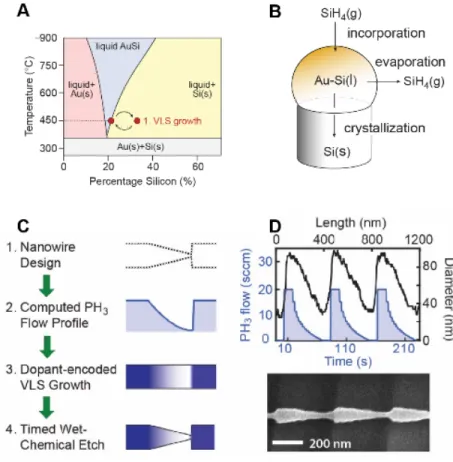
Typically silicon nanowires are grown using a vapor-liquid-solid (VLS) growth
mechanism. In this process, gold nanoparticles are deposited onto a silicon-nitride substrate,
where the size of these nanoparticles determines the diameter of the resultant nanowire. The
VLS growths for the nanowires used in my research are made possible by the gold-silicon binary
eutectic phase diagram. The
substrate is placed inside a
tube furnace, and brought to
low-vacuum, and then heated
above the gold-silicon
eutectic point. It is at this
point that the precursor gas,
Silane (SiH4) is flown into
the chamber. The gas
incorporates Silicon into the
gold nanoparticle, eventually
pushing the liquid
metal-semiconductor solution to the
point to silicon
supersaturation, causing
silicon to crash out and
crystalize. For this project a
Figure 1. VLS Growth of Nanowires and ENGRAVE
modified version of standard VLS growth is used, called Encoded Nanowire Growth and
Appearance through VLS Etching (ENGRAVE), wherein dopant precursors are flown in
addition to Silane. Diborane (B2H6) for p-type silicon and Phosphine (PH3) for n-type silicon.
While the silicon nanowire undergoes VLS growth, these dopants become incorporated in the
wire’s crystal structure. The dopant type and concentration can be varied along the length of the
nanowire via modulation in the flow rate of the dopant gases. A set of flow rates may be
preprogrammed for the various precursor gases, so that nanowire growth rate and dopant level
can be controlled and changed in situ. Concentrations high enough to achieve degenerate doping
levels, sufficient doping to treat a semiconductor as a conductor, are possible despite
necessitating
higher-than-equilibrium bulk solid solubility
limit concentrations. (1)
However there are a
variety of issues that an
ENGRAVE growth can undergo.
It is possible for the doping level
to deviate slightly from what was
programed. A common
occurrence in p-type nanowires
is gold depositing nonselectively
on sidewalls. Spikes in pressure
are known to cause kinking,
spontaneous changing in crystal
Figure X. Creating Nanowire Geometric Diodes
growth direction. Kinking can cause increases in resistance and nonlinear I-V characteristics.
When precursor gasses decompose on the surfaces of nanowires it can induce tapering. (1)
Once a silicon nanowire is grown using ENGRAVE, its geometry can be finely
controlled via wet chemical etching. Silicon’s reactivity to chemical etchants is highly
dependent on its dopant type and level. A buffered hydrofluoric acid (BHF) solution is used to
etch away a silicon nanowire’s native oxide layer. BHF etching can have different effects in for
intrinsic, n-type, and p-type silicon. In intrinsic and p-type silicon BHF does not significantly
etch the surface while in n-type silicon BHF does. However in all cases BHF can cause an
increase in surface roughness. In the case of both p-type and n-type silicon, resistivity to
potassium hydroxide (KOH) increases with dopant level, such that degenerately doped silicon
essentially doesn’t etch in dilute KOH. (1)
1.2 Electron Ratchets and Geometric Diodes
Electron ratchets are devices that through an intrinsic asymmetry, allow for directionally
nonlinear charge transport. The prototypical example of an electron ratchet is a diode.
Traditionally diodes are made using alternative p-type, n-type sections that form PN junctions.
PN junctions modify the band structure, such that a potential barrier energetically favors the flow
of charge carriers in one direction. An alternative to traditional diodes are geometric diodes,
which operate not due to potential barriers, but due to the shape of the device. In such devices
the encoded geometry, asymmetric on the scale of the mean free path of the primary charge
carrier, gives rise to anisotropic resistance. (2) The literature is still developing a proper
first type is also called a self-switching diode (SSDs), and the literature is backing off from
calling these geometric diodes. SSDs operate because the geometry of the device causes charges
to accumulate differently in the forward bias versus reverse bias regimes. (3) In reverse bias,
the accumulation of charges can increase the energy required to pass through small channels,
causing resistance to increase. In forward bias, these charges do not accumulate in such a way.
The second, and more official type of geometric diode is the ballistic device, where charge
transport is in the ballistic regime. In this regime charges are able to interact with boundaries in
the geometry of the device, causing non-linear charge transport akin to a funnel. (4)(5) This is
how silicon nanowire geometric diodes operate. To date, ballistic transport devices have only
been possible in materials with large mean free paths, and only at cold temperatures. Such as in
graphene. (4)(5) However to be made more practical, we aim to create these sorts of devices in
silicon, a material readily available and with infrastructure available to mass produce.
Additionally for practicality, they must be able to work at room temperature.
1.3 Motivation
Geometric diodes are incredibly useful for all of the same reasons that traditional diodes
are. Their nonlinear charge carrier transport allow for the rectification of AC signals, which has
a number of applications. There are issues with P-N junction diodes which geometric diodes can
solve. Due to the mechanics of a P-N junction there is a voltage that a signal must surpass before
the diode turns on (referred to as it’s turn-on voltage). The mechanism behind geometric diodes
does not rely on charge carriers overcoming some potential; therefore, they have theoretically
zero turn-on bias. This gives geometric diodes the ability to rectify small signals at low to zero
input bias when compared to P-N junctions. Secondly P-N junction diodes lose their
depletion region shrinking as frequency. Again, geometric diodes do not have such a constraint.
Due to their ultra-low capacitance, on the order of 10-17 F, their time constant allows for response
far into the THz. However, the flight time of charge carriers becomes a more substantial
constraint on frequency response, charge carriers must travel a sufficient distance over the span
of a wavelength, such that they interact with the geometry. Theoretically these interactions
should still occur substantially enough to give an asymmetric I-V curve into the THz. These
advantages geometric diodes have over P-N junctions, make them perfect candidates as
components in high-speed data transfer, rectennas, and battery-less devices.(3)(6)(7) Terahertz
electromagnetic waves approach the energy levels produced by ambient background radiation in
the environment, therefore diodes that are able to rectify this energy will be able to power
devices by pulling energy out of these background signals.(8)(9)(10) Before these wires can be
implemented in such devices their electronic characteristics must be investigated.
CHAPTER 2: PRELIMINARY WORK
2.1 n-Type Nanowire Geometric Diodes
ENGRAVE is capable of creating sawtooth structures in both p-type and n-type degenerately
doped silicon nanowires. Initally experiments were done using n-type nanowires due to the
increased mean-free-path of electrons over electron holes in silicon. Once these n-type wires
were grown and etched with the appropriate geometries they are transferred onto a marker
partern. Utilizing electron-beam (e-beam) lithography, contacts can be drawn precisely, using
PMMA as an e-beam resist. After developing, Ti-Pd contacts are deposited using e-beam
section, this way it is possible to
check whether or not the
contacts are ohmic. Non-ohmic
contacts can be caused by the
formation of schottky barriers,
due to an oxide layer forming
prior to metal deposition.(11)
To reduce the liklihood of this
the degenerately doped sections
of nanowires are etched in a
BHF solution to remove the
oxide, immediately before the
devices are placed into the
e-beam evaporator. The pairs of
contacts on either side are also
used to measure the resistivity of
the degenerately doped sections,
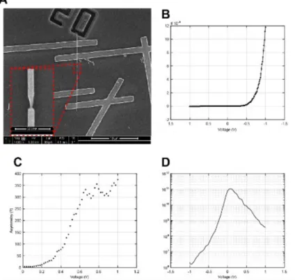
this allows us to guage the doping level of the nanowire and ensure the contacts are ohmic. The
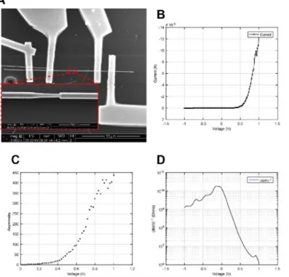
inner two contacts are used to measure the diode properties of the device. Figure 3B shows an
example I-V curve of an n-type geometric diode. All DC measurments are done using a source
measure unit (SMU), varying the voltage such there are an odd number of total data points of
equal spacing, centered on zero. Data is collected with this spacing to ensure that if there is a
value for some forward bias then there is another at that same reverse bias. These I-V curve
Figure 3. Sample n-Type DC Measurements.
measurements are used to define the asymmetry of a device, asymmetry here is defined as the
current of a diode at some positive bias divided be the current at that negative bias, an example is
shown in Figure 3C.
𝛼𝛼(𝑉𝑉) =𝐼𝐼𝐼𝐼(+(−𝑉𝑉𝑉𝑉))
I-V curves are also used to calculate a different parameter, the differential resistance of a
geometric diode. The differential resistance is found by numerically calculating the derivative of
voltage with respect to current.
𝑅𝑅𝑑𝑑𝑑𝑑𝑑𝑑𝑑𝑑 = 𝑑𝑑𝑉𝑉𝑑𝑑𝐼𝐼
For geometric diodes that show nonnegligible asymmetry, the differential resistance is shown to
be approximtaely a decaying exponential. This exponential decay implies that the performance
of a geometric diode will improve as the voltage drop across the component increases. Due to
the small size of silicon nanowires, ~100nm, and the high resistivity of sawtooth sections in the
reverse bias and low bias regimes, they often are destroyed at voltages above several volts. The
voltage at which a device is destroyed varies wildly from wire to wire. Figure 3 demonstrates
DC measurements for single sawtooth devices, however due to the nonlinear resistance in
forward or reverse bias regimes, the electronic properties of nanowire geometric diodes in
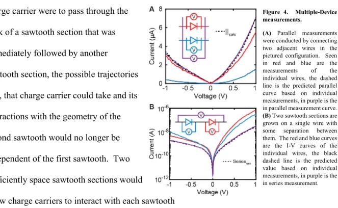
parallel or in series are of great interest. Additionally due to the devices operating purely due to
interactions with the geometry, it was not initially certain whether geometric diode circuits, such
as two wires in parallel, or two wires in series, would operate as one would expect two
traditional electronic components to work. The primary reason for doubting this is due to the
charge carrier were to pass through the
neck of a sawtooth section that was
immediately followed by another
sawtooth section, the possible trajectories
that, that charge carrier could take and its
interactions with the geometry of the
second sawtooth would no longer be
independent of the first sawtooth. Two
sufficiently space sawtooth sections would
allow charge carriers to interact with each sawtooth
functionally indpendent of each other. However Figure 4 demonstrates the I-V curves of such
devices and the I-V curves of the individual nanowires that build those circuits. Figure 4A
shows the measuremtns for two wires in parallel. When two wires of different asymmetry values
are measured in parallel, the two combined have an asymmetry approximately of the lower of the
two. However this configuration decreases the overall resistance, increasing current. Lowering
resistance may also help in situations where impedance matching is important, such as high
frequency rectification. Figure 4B shows the measuremtents for two wires in series. When two
wires are in series, the overall current decreases. This is an artifact of the exponential decay of a
nanowire geometric diode’s differential resistance. For the same bias the voltage drop across
each sawtooth section is lower therefore the total current decreases. This does have the added
benefit of reducing the likelyhood that a nanowire device is destroyed due to too high of a
voltage. The load is spread across the length of the wire rather than a single sawtooth, giving
series wires use in high voltage applications. Additionally since series wires have the capability
Figure 4. Multiple-Device measurements.
to be grown and etched on the same wire, with a variety of sawtooth geometries, a single wire
device is highly tunable. The measurements of two geometric diodes in parallel shows that the
combined I-V curve has higher current than each individual measurement. As the voltage drop
across each individual wire is constant each individual device is in less danger of being
destroyed, while allowing for higher output current.
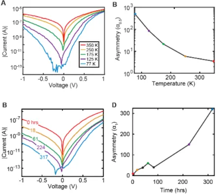
There are other methods available to change diode performance. Teamperature and
Surface Treatment. Using liquid nitrogen, DC measurement could be taken at a variety of
temperatures. Figure 5A demonstrates the I-V curves of a nanowire over temperatures ranging
from 350K to 77K. As temperature decreases, there is a noticable increase in measured
asymmetry and simultaneous drop
in current. The asymmetry
improved, most likely due to the
change in mean free path. Though
not pictured, low temperatures also
caused nanowire electronic
characteristics to become sensitive
to light. This is likely due to light
mediated traped states affecting
carrier transport. As temperature
decreases current decreases, this can
be explained by there being less
availble charge carriers, many being
frozen out. (12)
Figure 5. Surface Treatment and Low Temperature Measurements.
As the primary benefit of using silicon nanowire geometric diodes over graphene or a
2DEG (2)(4), is that nanowires respond at room temperature, it is counter-productedive to rely
on increasing performance by lowering temperatures. Therefore we look towards surface
treatments as a way to modify nanowire geometric diode electronic properties. In Figure 5C,
shown are the I-V curves for a nanowire after sitting in air intermittenly, to a maximum of 317
hours. As the oxide layer is removed by the etching process, the oxide layer must grow back
over time. Introduction of surface oxide is shown to increase asymetry significantly. There may
be several reasons that an oxide layer affects asymmetry to this degree. First is that, as oxide
grows, it must replace unoxidized silicon, thereby shrinking the geometries which has been
shown to increase both resistance and asymmetry. Additionally band bending on the silicon,
silicon-oxide interface can cause charges to accumulate as a charge double layer.(13) The
potential due to these charges changes how charge carriers interact with the boundaries of the
device, effectively smoothing out the surface and leading to more specular reflection. Different
surface treatments can passivate the exterior of the nanowire or cause different types of charges
to accumulate on the interior surface of the nanowire. Idealy, a surface treatment can be chosen
such that the opposite charge of the primary charge carrier will accumulate, increasing the rate
that charge carriers interact with the geometry, improving asymmetry.
2.2 Modeling Geometric Diodes
It is typical for situations involving ballistic conduction to be simulated using Monte
Carlo methods. (4) One such method, developed by a previous undergraduate researcher,
simulated the motion of charge carriers allowing a charge to traverse a silicon nanowire across
charge a momentum vector picked from a distribution accounting for thermal, Brownian motion
and directional momentum from an applied electric field. After moving for approximately the
mean free time, the charge is assigned a new, randomly selected momentum and travels another
time step. In the case that these charges intersect with a boundary of the nanowire device before
they experience a scattering
event, the charge will scatter
specularly. An effective current
is able to be calculated by
directly counting the flux of
charges that pass through the
aperture of the geometric diode.
This model is able to accurately
represent both the physics and
the geometry involved in
nanowire geometric diodes,
however it requires many time
steps and iterations to converge,
and the code written for this
simulation had
difficult-to-correct errors.
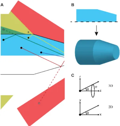
In order to find a new way to model ballistic conduction devices, an analytical expression
was sought to calculate effective currents, and therefore the asymmetry of nanowires with given
geometries. The benefit over an analytic function is that the properties of a device can be
Figure 6. Analytical Model Formulation
determined after a short calculation, taking minutes, as opposed to the hours Monte Carlo takes
to converge. The analytic models works as the following, a charge carrier flux is calculated by
computing a volume integral of an integral of a weight function from the lower angle to upper
angle of charge trajectories that pass through the neck. Due to the cylindrical symmetry of the
nanowire, the interior region of integration can be simplified to a 2-dimensional slice with an
introduction of a 2𝜋𝜋𝜋𝜋 term in the volume integral. This degeneracy in position states can also be
used to simplify out-of-plane trajectories, effectively rotating any trajectory back into the
integration plane, further simplifying calculations. To account for trajectories that reflect
specularly off of the boundaries of the device, the interior region of integration is used to
generate 8 additional integration regions by applying reflection transformations and geometric
constraints.
𝐼𝐼𝑒𝑒𝑑𝑑𝑑𝑑 =2𝑉𝑉𝜋𝜋
0 � � 𝑑𝑑𝜋𝜋𝑑𝑑𝑑𝑑 � 𝑊𝑊𝑠𝑠(𝜃𝜃)𝑑𝑑𝜃𝜃 𝜃𝜃𝑠𝑠𝑠𝑠
𝜃𝜃𝑠𝑠𝑠𝑠 𝜏𝜏𝑠𝑠
𝑠𝑠
Where V0 is the volume of the inside of the nanowire, s is one of nine total regions of
integration, Ws(θ) is a weight function used to prescribe probability distributions to the potential
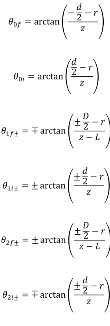
trajectories of charge carriers. θi and θf are the minimum most and maximum most angles by
which a charge carrier can travel in a straight line and pass through the neck of the diode. The
reflects off a boundary and which boundary it reflects off of if it does. These angles are
functions of position, such that the center of the neck is the origin, and are calculated as such.
𝜃𝜃0𝑑𝑑 = arctan�
− 𝑑𝑑2− 𝜋𝜋
𝑑𝑑 �
𝜃𝜃0𝑑𝑑 = arctan� 𝑑𝑑
2− 𝜋𝜋
𝑑𝑑 �
𝜃𝜃1𝑑𝑑± =∓arctan�
±𝐷𝐷2 − 𝜋𝜋 𝑑𝑑 − 𝐿𝐿 �
𝜃𝜃1𝑑𝑑±= ± arctan�
±𝑑𝑑2− 𝜋𝜋
𝑑𝑑 �
𝜃𝜃2𝑑𝑑±= ± arctan�
±𝐷𝐷2 − 𝜋𝜋 𝑑𝑑 − 𝐿𝐿 �
𝜃𝜃2𝑑𝑑±= ∓arctan�
±𝑑𝑑2− 𝜋𝜋
𝑑𝑑 �
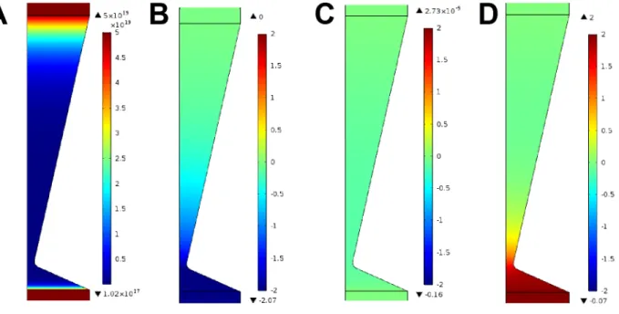
2.3 COMSOL Simulations
The above model developed to predict diode performance’s dependence on geometry,
works well on its own, but ignores much of the physics occurring within the device. For instance
the model neglects band structure, electrostatics, and effects due to doping. However with
COMSOL simulations we are able to estimate the contributions of these sorts of effects towards
Figure 7. Analytical Model Results.
the IV characteristics of nanowire devices. Conveniently, COMSOL is unable to account for the
ballistic interactions of charge carriers and boundaries. Therefore both models can be combined
to give a more complete picture of the electronic properties of the geometric diodes. The
Cahoon group as a specially made COMSOL model for the use of simulating silicon nanowire
devices. Silicon nanowires are well suited for finite-difference modeling such as COMSOL due
to their small size and simple geometries. Similar to the analytical model the nanowire is
constructed as a two-dimensional region that can be rotated into a full wire due to its cylindrical
symmetry. Sweeping over applied biases and nanowire geometries, the drift and diffusion of
charge carriers are calculated accounting for Shockley-Read-Hall, Auger, and surface
recombination. Additionally effects due to the encoded degenerately doped regions such as band
gap renormalization is included in calculations. Previous simulations by the Cahoon group,
verified by experiment, show that this model can accurately predict the electronic properties of
Figure 8. COMSOL Simulations
silicon nanowire devices. These simulations also show how space charge density and electric
field strength through the wire are highly dependent on the doping level.(14)
CHAPTER 3: CHARACTERIZING P-TYPE GEOMETRIC DIODES
3.1 DC Measurements
In order to gain more insight to the mechanism behind silicon nanowire geometric diodes,
p-type devices were developed and measured. The process to make p-type ENGRAVE
nanowires is essentially the same as n-type. Notable changes in device fabrication is the change
of dopant precursor gas from phosphine (PH3) to diborane (B2H6) and p-type degenerately doped
sections are more susceptible to non-ohmic contacts during e-beam evaporation. (15) In p-type
nanowires, the primary charge carrier is the electron hole, as opposed to the electron in n-type.
This means that charge carriers in p-type nanowire geometric diodes will have a different mean
free path and charge.(11) The change in mean free path allows us to explorethe parameter space
for geometric diodes, as well as check the veracity of the implementation of mean free path in
the analytic model. The positive primary charge carriers will interact with surfaces in the
opposite manner as the negative charge carriers in n-type silicon. Additionally it has been
direction than n-type, this is due
to the opposite charge of the
primary charge carrier(1) and the
fact that electron holes, not
electrons, are interacting with the
geometry. In Figure 7C, the
analytical model predicts that a
p-type silicon has a favorable
mean free path. Figure 9
demonstrates the DC
measurements used to
characterize th electronic
properties of p-type geometric
diodes. The measurements are
done with the same procedure as
for n-type, seen in Figure 3. To
date, p-type devices have shown higher asymmetries than measured in n-type devices, giving
credence to the benefit of a lower mean-free-path. Additionally these devices also have higher
current than one would expect of n-type devices of similar asymmetry values.
So far p-type silicon nanowire geometric diodes have shown promise as alternatives to
the traditional P-N junction diodes. Geometric diodes had previously been theorized to have
zero turn-on voltage and potential requency response into the THz. Experiments have
demonstrated that these devices can output high currents in the forward bias, while being
Figure 9. Sample p-Type DC Measurements.
effectively off in the reverse, while truly having zero turn-on voltage. The project has some
shortcomings, especially in device fabrication, where gated devices and high frequency devices
have not been successfully fabricated. The next steps for this project will be to refine the
fabrication process and show that p-type silicon nanowire diodes can respond at Thz frequencies.
More devices with varied geometries must be fabricated to explore the parameter space of diode
electronic properties and give more experimental credence to the analytical model. Once more
evidence for the analytical model for ballistically conducting devices is generated, the model can
(1-19)
1. J. D. Christesen, C. W. Pinion, E. M. Grumstrup, J. M. Papanikolas, J. F. Cahoon, Synthetically Encoding 10 nm Morphology in Silicon Nanowires. Nano Lett. 13, 6281-6286 (2013).
2. A. M. Song, Electron ratchet effect in semiconductor devices and artificial materials with broken centrosymmetry. Appl. Phys. A 75, 229-235 (2002).
3. A. Westlund et al., Graphene self-switching diodes as zero-bias microwave detectors. Appl. Phys.
Lett. 106, 093116 (2015).
4. Z. Zhu, S. Joshi, S. Grover, G. Moddel, Graphene geometric diodes for terahertz rectennas. J.
Phys. D: Appl. Phys. 46, 185101 (2013).
5. G. Auton et al., Terahertz Detection and Imaging Using Graphene Ballistic Rectifiers. Nano Lett.
17, 7015-7020 (2017).
6. E. S. Kannan, I. Bisotto, J. C. Portal, T. J. Beck, L. Jalabert, Energy free microwave based signal communication using ratchet effect. Appl. Phys. Lett. 101, 143504 (2012).
7. C. Balocco et al., Microwave detection at 110 GHz by nanowires with broken symmetry. Nano
Lett. 5, 1423-1427 (2005).
8. S. J. Byrnes, R. Blanchard, F. Capasso, Harvesting Renewable Energy from Earth’s mid-infrared Emissions. Proc. Natl. Acad. Sci. 111, 3927-3932 (2014).
9. N. Kaur, N. Sharma, N. Kumar, RF Energy Harvesting and Storage System of Rectenna: A Review.
Indian Journal of Science and Technology 11, 1-5 (2018).
10. B. Clerckx et al., Fundamentals of Wireless Information and Power Transfer: From RF Energy Harvester Models to Signal and System Designs. IEEE Journal on Selected Areas in
Communications 37, 4-33 (2019).
11. S. M. Sze, K. K. Ng, Physics of Semiconductor Devices. (Wiley, 2006).
12. S. S. Li, W. R. Thurber, The dopant density and temperature dependence of electron mobility and resistivity in n-type silicon. Solid-State Electron. 20, 609-616 (1977).
13. E. B. Ramayya, D. Vasileska, S. M. Goodnick, I. Knezevic, Electron Mobility in Silicon Nanowires.
IEEE Trans. Nanotechnol. 6, 113-117 (2007).
14. X. Z. Joseph D. Christesen, Christopher W. Pinion, Thomas A. Celano, Cory J. Flynn, and James F. Cahoon, Design Principles for Photovoltaic Devices Based on Si Nanowires with Axial or Radial p-n Jup-nctiop-ns. Nano Lett. 12, (2012).
15. F. J. Morin, J. P. Maita, Electrical Properties of Silicon Containing Arsenic and Boron. Physical
Review 96, 28-35 (1954).
16. D. Dragoman, M. Dragoman, Geometrically induced rectification in two-dimensional ballistic nanodevices. J. Phys. D: Appl. Phys. 46, 055306 (2013).
17. P. Zhang, D. M. H. Hung, An analytical model for ballistic diode based on asymmetric geometry.
J. Appl. Phys. 115, 204908 (2014).
18. W. Saeed, N. Shoaib, H. M. Cheema, M. U. Khan, RF Energy Harvesting for Ubiquitous, Zero Power Wireless Sensors. International Journal of Antennas and Propagation 2018, 16 (2018). 19. U. Muncuk, K. Alemdar, J. D. Sarode, K. R. Chowdhury, Multiband Ambient RF Energy Harvesting