An Efficient Programmable 10 Gigabit Ethernet Network Interface Card
Paul Willmann Hyong-youb Kim Scott Rixner
Rice University
Houston, TX
{
willmann,hykim,rixner
}
@rice.edu
Vijay S. Pai
Purdue University
West Lafayette, IN
[email protected]
Abstract
This paper explores the hardware and software mech-anisms necessary for an efficient programmable 10 Giga-bit Ethernet network interface card. Network interface pro-cessing requires support for the following characteristics: a large volume of frame data, frequently accessed frame metadata, and high frame rate processing. This paper pro-poses three mechanisms to improve programmable network interface efficiency. First, a partitioned memory organiza-tion enables low-latency access to control data and high-bandwidth access to frame contents from a high-capacity memory. Second, a novel distributed task-queue mecha-nism enables parallelization of frame processing across many low-frequency cores, while using software to main-tain total frame ordering. Finally, the addition of two new atomic read-modify-write instructions reduces frame order-ing overheads by 50%. Combinorder-ing these hardware and soft-ware mechanisms enables a network interface card to satu-rate a full-duplex 10 Gb/s Ethernet link by utilizing 6 pro-cessor cores and 4 banks of on-chip SRAM operating at 166 MHz, along with external 500 MHz GDDR SDRAM.
1. Introduction
As Internet link speeds continue to grow exponen-tially, network servers will soon have the opportunity to utilize 10 Gb/s Ethernet to connect to the Internet. A pro-grammable network interface card (NIC) would provide a flexible interface to such high-bandwidth Ethernet links. However, the design of a programmable NIC faces sev-eral software and architectural challenges. These challenges stem from the large volume of frame data, the require-ment for low-latency access to frame metadata, and the raw computational requirements for frame processing. Fur-thermore, unlike a network interface in a router, a net-work interface card in a server must also tolerate high This work is supported in part by the NSF under Grant Nos. CCR-0209174, CCR-0238187, and ACI-0305691 and by donations from AMD.
latency communication with the system’s host proces-sor for all incoming and outgoing frames. These challenges must all be met subject to the constraints of a periph-eral within the server, limiting the area and power con-sumption of the NIC.
A 10 Gb/s programmable NIC must be able to support at least 4.8 Gb/s of control data bandwidth and 39.5 Gb/s of frame data bandwidth to achieve full-duplex line rates for maximum-sized (1518 byte) Ethernet frames. The con-trol data must be accessed by the processor cores in order to process frames that have been received or are about to be transmitted. On the other hand, the frame data must simply be stored temporarily in either the transmit or receive buffer as it waits to be transferred to the Ethernet or the system host. Therefore, control data must be accessed with low la-tency, so as not to disrupt performance, and frame data must be accessed with high bandwidth, so as to maximize trans-fer speeds. These two competing requirements motivate the separation of control data and frame data.
Network interfaces tolerate the long latency of commu-nication between the system host and the network inter-face using an event mechanism. The event model enables the NIC to exploit task-level parallelism to overlap differ-ent stages of frame processing with high latency communi-cations. However, task-level parallelism is not sufficient to meet the computation rates of 10 Gb/s Ethernet. Instead, a frame-parallel organization enables higher levels of paral-lelism by permitting different frames in the same stage of frame processing to proceed concurrently. However, a new event-queue mechanism is required to control dispatching of events among parallel processors.
This paper presents an efficient 10 Gb/s Ethernet net-work interface controller architecture. Three mechanisms improve programmable network interface efficiency. First, a partitioned memory organization enables low-latency ac-cess to control data and high-bandwidth acac-cess to frame contents from a high-capacity memory. Second, a novel dis-tributed task-queue mechanism enables parallelization of frame processing across many low-frequency cores, while using software to maintain total frame ordering. Finally,
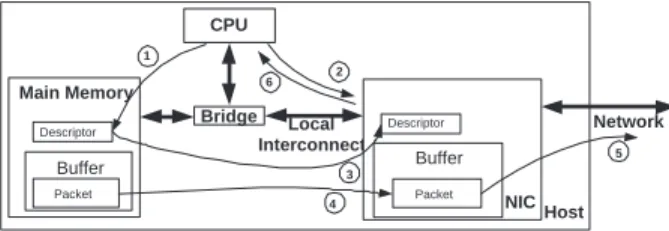
Host CPU Main Memory Local Interconnect NIC Buffer Network 5 2 6 Packet 3 Packet Descriptor Buffer Descriptor Bridge 1 4
Figure 1. Steps involved in sending a packet.
the addition of two new atomic read-modify-write instruc-tions reduces frame ordering overheads by 50%. Combin-ing these hardware and software mechanisms enables a simulated network interface card to saturate a full-duplex 10 Gb/s Ethernet link by utilizing 6 processor cores and 4 banks of on-chip SRAM operating at 166 MHz, along with external 500 MHz GDDR SDRAM.
The following section explains the behavior of a network interface, including its operation and its computation and bandwidth requirements. Section 3 describes how network interface firmware can be parallelized efficiently using an event queue mechanism. Section 4 then describes the archi-tecture of the proposed 10 Gigabit Ethernet controller. Sec-tion 5 describes the methodology used to evaluate the archi-tecture, and Section 6 evaluates the proposed architecture. Section 7 describes previous work in the area, and Section 8 concludes the paper.
2. Background
The host operating system of a network server uses the network interface to send and receive packets. The operat-ing system stores and retrieves data directly to or from the main memory, and the NIC transfers this data to or from its own local transmit and receive buffers. Sending and receiv-ing data is handled cooperatively by the NIC and the de-vice driver in the operating system, which notify each other when data is ready to be sent or has just been received.
2.1. Network Interface Processing
Sending a packet requires the steps shown in Figure 1. In step 1, the device driver first creates a buffer descrip-tor, which contains the starting memory address and length of the packet that is to be sent, along with additional flags to specify options or commands. If a packet consists of mul-tiple non-contiguous regions of memory, the device driver creates multiple buffer descriptors. The device driver then writes to a memory-mapped register on the NIC with infor-mation about the new buffer descriptors, in step 2. In step 3 of the figure, the NIC initiates one or more direct memory access (DMA) transfers to retrieve the descriptors. Then, in step 4, the NIC initiates one or more DMA transfers to move
Host CPU Main Memory Local Interconnect NIC Buffer Network 1 2 4 Packet 3 Packet Descriptor Buffer Descriptor Bridge
Figure 2. Steps involved in receiving a packet.
the actual packet data from the main memory into its trans-mit buffer using the address and length information in the buffer descriptors. After the packet is transferred, the NIC sends the packet out onto the network through its medium access control (MAC) unit in step 5. The MAC unit is re-sponsible for implementing the link-level protocol for the underlying network such as Ethernet. Finally, in step 6, the NIC informs the device driver that the descriptor has been processed, possibly by interrupting the CPU.
Receiving packets is analogous to sending them, but the device driver must also preallocate a pool of main-memory buffers for arriving packets. Because the system cannot an-ticipate when packets will arrive or what their size will be, the device driver continually allocates free buffers and and notifies the NIC of buffer availability using buffer descrip-tors. The notification and buffer-descriptor retrieval pro-cesses happen just as in the send case, following steps 1 through 3 of Figure 1.
Figure 2 depicts the steps for receiving a packet from the network into preallocated receive buffers. In step 1, a packet arriving over the network is received by the MAC unit and stored in the NIC’s local receive buffer. In step 2, the NIC initiates a DMA transfer of the packet into a pre-allocated main memory buffer. In step 3, the NIC produces a buffer descriptor with the resulting address and length of the received packet and initiates a DMA transfer of the de-scriptor to the main memory, where it can be accessed by the device driver. Finally, in step 4, the NIC notifies the de-vice driver about the new packet and descriptor, typically through an interrupt. The device driver may then check the number of unused receive buffers in the main memory and replenish the pool for future packets.
To send and receive frames, as described here, a grammable Ethernet controller would need one or more pro-cessing cores and several specialized hardware assist units that efficiently transfer data to and from the local intercon-nect and the network. Table 1 shows the per-frame computa-tion and memory requirements of such a programmable net-work interface when carrying out the steps in Figure 1 and Figure 2. The table’s fractional instruction and data-access counts are artifacts of the way several frames are processed with just one function call. The data shown is collected from actual network interface firmware, but does not include any implementation specific overheads such as parallelization
Function Instructions Data Accesses
Fetch Send BD 24.5 10.6
Send Frame 256.9 90.0
Fetch Receive BD 12.1 4.1
Receive Frame 241.0 80.8
Table 1. Average number of instructions and data accesses to send and receive one Ethernet frame.
overheads. The Fetch Send BD and Fetch Receive BD tasks fetch buffer descriptors from the main memory that specify the location of frames to be sent or of preallocated receive buffers (step 3 of Figure 1). Send Frame and Receive Frame implement steps 4-6 of Figure 1 and 1-4 of Figure 2, re-spectively. Note that Fetch Send BD and Fetch Receive BD transfer multiple buffer descriptors (32 and 16 descriptors) through a single DMA, and the instruction and data access counts shown in the table are weighted to show the average counts per frame. Furthermore, each sent frame typically re-quires two buffer descriptors because the frame consists of two discontiguous memory regions, one for the frame head-ers and one for the payload.
A full-duplex 10 Gb/s link can deliver maximum-sized 1518-byte frames at the rate of 812,744 frames per second in each direction. Hence, sending frames at this rate using the tasks in Table 1 requires 229 million instructions per second (MIPS) and 2.6 Gb/s of data bandwidth. Similarly, receiving frames at the line rate requires 206 MIPS and 2.2 Gb/s of data bandwidth. Therefore, a full-duplex 10 Gi-gabit Ethernet controller must be able to sustain 435 MIPS and 4.8 Gb/s of data bandwidth. However, this does not in-clude the bandwidth requirements for transferring the frame data itself. Each sent or received frame must be first stored into the local memory of the NIC and then read from the memory. For example, to send a frame, the NIC first trans-fers the frame from the main memory into the local mem-ory, and then the MAC unit reads the frame from the lo-cal memory. Thus, sending and receiving maximum-sized frames at 10 Gb/s require 39.5 Gb/s of data bandwidth. This is slightly less than the overall link bandwidth would sug-gest (2*2*10 Gb/s) because data cannot be sent during the Ethernet interframe gap.
2.2. Instruction-level Parallelism
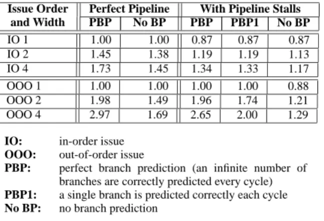
Though the lower bound on raw computation established in the previous section is useful, it provides little insight into the most efficient processor architecture for network interfaces. It is important to also understand how much instruction-level parallelism can be exploited in such net-work interface firmware. There are several factors that can limit the obtainable instructions per cycle (IPC) of a partic-ular processor running network interface firmware. The ma-jor factors considered here are whether the processor issues
Issue Order Perfect Pipeline With Pipeline Stalls
and Width PBP No BP PBP PBP1 No BP IO 1 1.00 1.00 0.87 0.87 0.87 IO 2 1.45 1.38 1.19 1.19 1.13 IO 4 1.73 1.45 1.34 1.33 1.17 OOO 1 1.00 1.00 1.00 1.00 0.88 OOO 2 1.98 1.49 1.96 1.74 1.21 OOO 4 2.97 1.69 2.65 2.00 1.29
IO: in-order issue
OOO: out-of-order issue
PBP: perfect branch prediction (an infinite number of branches are correctly predicted every cycle)
PBP1: a single branch is predicted correctly each cycle
No BP: no branch prediction
Table 2. Theoretical peak IPCs of NIC firmware for different processor configurations.
instructions in-order or out-of-order, the number of instruc-tions that can be issued per cycle, whether or not branch prediction is used, and the structure of the pipeline.
Table 2 gives the IPC of NIC firmware for different the-oretical processor configurations. These figures were ob-tained by performing an offline analysis of a dynamic in-struction trace of idealized NIC firmware with paralleliza-tion overheads removed. The firmware was compiled for a MIPS R4000 processor, which features one branch delay slot.
The table shows the IPC limits for both in-order and out-of-order cores. For each type, these limits are shown for a processor that has a perfect pipeline and for one that has a pipeline that experiences dependence-based stalls. In the perfect pipeline, all instructions complete in a single cy-cle, so the only limit on IPC is that instructions that de-pend on each other cannot issue during the same cycle. For a more realistic limit on IPC, a typical five stage pipeline with all forwarding paths is modeled. In this pipeline, load-use sequences would caload-use a pipeline stall, and only one memory operation can issue per cycle. In addition to these pipeline configurations, three branch prediction strategies are modeled. For the perfect branch predictor, any num-ber of branches up to the issue width can be correctly pre-dicted on every cycle. When there is no branch prediction, a branch stops any further instructions from issuing until the next cycle. The “PBP1” predictor simply allows only a sin-gle branch per cycle to be perfectly predicted.
The table shows two obvious and well-known trends. For an in-order processor, it is more important to eliminate pipeline hazards than to predict branches. Conversely, for an out-of-order processor, it is more important to accurately predict branches than to eliminate pipeline hazards. More importantly, however, the table shows that the complex-ity required to improve the processor’s performance may not be worth the cost for an embedded system. For exam-ple, consider an in-order processor with no branch predic-tion and including pipeline stalls. Such a processor could
achieve an IPC of 0.87. In contrast, an out-of-order proces-sor with an issue width of two and perfect branch predic-tion of one branch per cycle could only achieve an IPC of 1.74. While this is twice the performance of the in-order core, this core has significantly higher complexity. It would need a wide issue window that must keep track of instruc-tion dependencies and select two instrucinstruc-tions per cycle. It would also need a register renaming mechanism and a re-order buffer to allow instructions to execute out-of-re-order. And, it would require a fairly complex branch predictor to approach the performance of a perfect branch predictor. All of this complexity adds area, delay, and power dissipation to the out-of-order core.
For an area- and power-constrained embedded system, it is likely to be more efficient to try to capture parallelism through the use of multiple processing cores, rather than by more complex cores. If the out-of-order core costs twice as much as the in-order core, and there is enough coarse-grained parallelism, it makes more sense to use two simple in-order cores. Furthermore, the table shows that increas-ing the IPC significantly beyond the level achieved by the two-wide out-of-order core requires significant additional cost, such as predicting multiple branches per cycle or issu-ing four instructions per cycle. This would further inflate the area, delay, and power dissipation of the core, making mul-tiple simple cores even more attractive.
Since the firmware for a network interface exhibits abun-dant parallelism that can be exploited by multiple cores, this data motivates the use of simple, single-issue, in-order pro-cessing cores as the base propro-cessing element for a network interface. This will minimize the complexity, and therefore the area, delay, and power dissipation of the system.
2.3. Data Memory System Design
The combination of parallel cores and hardware assists requires a multiprocessor memory system that allows the simple processor cores to access their data and instructions with low latency to avoid pipeline stalls while also allow-ing frame data to be transferred at line rate. Since the frame data is not accessed by the processing engines of the net-work interface, it can be stored in a high-bandwidth off-chip memory. However, the instructions and frame metadata ac-cessed by the processor must be stored in a low-latency, ran-dom access memory. Because instructions are read-only, ac-cessed only by the processors, and have a small working set, per-processor instruction caches are a natural solution for low-latency instruction access. The frame metadata also has a small working set, fitting entirely in 100 KB. How-ever, the metadata must be read and written by both the pro-cessors and the assists. Per-processor coherent caches are a well-known method for providing low-latency data access in multiprocessor systems. Caches are also transparent to
16B0 32B 64B 128B 256B 512B 1KB 2KB 4KB 8KB 16KB 32KB 10 20 30 40 50 60
Cache size (Bytes)
Hit Ratio (Percent)
Figure 3. Cache hit ratio for 6-core configuration with MESI coherence.
the programmer, enabling ease of programming. Each pro-cessor and assist could have its own private cache for frame metadata, with frame data set to bypass the caches in or-der to avoid pollution.
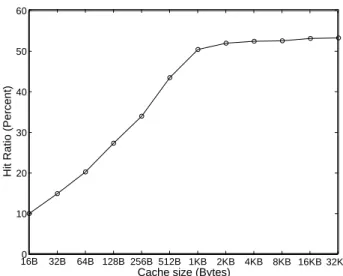
Despite the advantages of coherent caches, these struc-tures also have several disadvantages. Caches waste space by requiring tag arrays in addition to the data arrays that hold the actual content. Caching also wastes space by repli-cating the same widely-read data across the private caches of several processors. All coherence schemes add complex-ity and resource occupancy at the controller. Finally, caches are only effective given enough temporal or spatial local-ity and given the absence of excessive read-write sharing. To test the effectiveness of coherent caches with respect to NIC processing, separate data access traces were collected for each processor core and hardware assist in a 6-core con-figuration. The traces were gathered while running the NIC processing functions described in Section 2.1 and while us-ing the parallelization mechanisms detailed in Section 3.3. These traces were filtered to include only frame metadata and then analyzed using SMPCache, a trace-driven cache coherence simulator [23]. Since SMPCache can only model a maximum of 8 per-processor caches, the DMA read and write assist traces were interleaved to form a single trace, as were the MAC transmit and receive traces.
Figure 3 shows the effectiveness of caches in this 6-core configuration. All caches studied are fully-associative with LRU replacement for optimistic results on caching. Additionally, a line size of only 16 bytes is used to avoid false sharing. The figure shows experiments varying the per-processor cache sizes from 16 bytes to 32 KB with a MESI protocol in all cases. The curve in Figure 3 shows the col-lective cache hit ratio of all of the caches, which never goes
above 55%. The low hit ratio is not caused by excessive in-validations; for each experiment, fewer than 1% of write ac-cesses cause an invalidation in another cache. Rather, there is little locality in network interface firmware, so caching is ineffective.
An alternative solution, commonly used in embed-ded systems, is the use of a program-controlled scratchpad memory. This is a small region of on-chip memory ded-icated for low-latency accesses, but all contents must be explicitly managed by the program. Such a scratch-pad memory operating at 200 MHz with one 32-bit port would provide 6.4 Gb/s of control data bandwidth, slightly more than the required 4.8 Gb/s. However, simultane-ous accesses from multiple processors would incur queue-ing delays. These delays can be avoided by splittqueue-ing the scratchpad into multiple banks, providing excess band-width to reduce latency. A banked scratchpad requires an interconnection network between the processors and as-sists on one side and the scratchpads on the other. Such net-works yield a tradeoff between area and latency, with a crossbar requiring at least an extra cycle of latency and sim-pler networks requiring more. On the other hand, the scratchpad avoids the waste, complexity, and replica-tion of caches and coherence.
Since the processors do not need to access frame data, frame data does not need to be stored in a low-latency mem-ory structure. Furthermore, frame data is always accessed as four 10 Gb/s sequential streams with each stream coming from one assist unit. Current graphics DDR SDRAM can provide sufficient bandwidth for all four of these streams. The Micron MT44H8M32, for example, can operate at speeds up to 600 MHz, yielding a peak bandwidth per pin of 1.2 Gb/s [17]. Each of these SDRAMs has 32 data pins; two of them together can provide a peak bandwidth of 76.8 Gb/s. The streaming nature of the hardware assists in this architecture also make it possible to achieve near peak bandwidth from such SDRAM. By providing enough buffering for two maximum-sized frames in each assist, data can be transferred between the assists and the SDRAM up to 1518 bytes at a time. These transfers are to consecutive memory locations, so using an arbitration scheme that al-lows the assists to sustain such bursts will incur very few row activations in the SDRAM and allow peak bandwidth to be achieved during these bursts.
3. Parallel Firmware
As discussed in the previous section, an efficient pro-grammable 10 Gb/s network interface must use paral-lel computation cores, per-processor instruction caches, scratchpad memories for control data, and high-bandwidth SDRAM for frame contents. In order to successfully uti-lize such an architecture, however, the Ethernet firmware
running on the interface must be parallelized appropri-ately. The traditional approach of parallelizing solely across tasks is not scalable in this domain, so frame-level paral-lelism is necessary to achieve 10 Gb/s rates.
3.1. Event-based Processing
As depicted in Figures 1 and 2, network interfaces expe-rience significant latencies when carrying out the steps nec-essary to send and receive frames; most of these latencies stem from requests to access host memory via DMA. To tolerate the long latencies of interactions with the host, NIC firmware uses an event-based processing model in which the steps outlined in Figures 1 and 2 map to separate events. Upon the triggering of an event, the firmware runs a specific event handler function for that type of event. Events may be triggered by hardware completion notifications (e.g., packet arrival, DMA completion) or by other event handler func-tions that wish to trigger a software event.
3.2. Task-level Parallel Firmware
Previous network interface firmware paralleliza-tions leveraged the event model and Alteon’s Tigon-II event notification mechanism to run different event handlers con-currently [2, 13]. The Tigon-II Ethernet controller uses a hardware-controlled event register to indicate which types of events are pending. An event register is a bit vector in which each bit corresponds to a type of event. A set bit in-dicates that there are one or more events of that type that need processing.
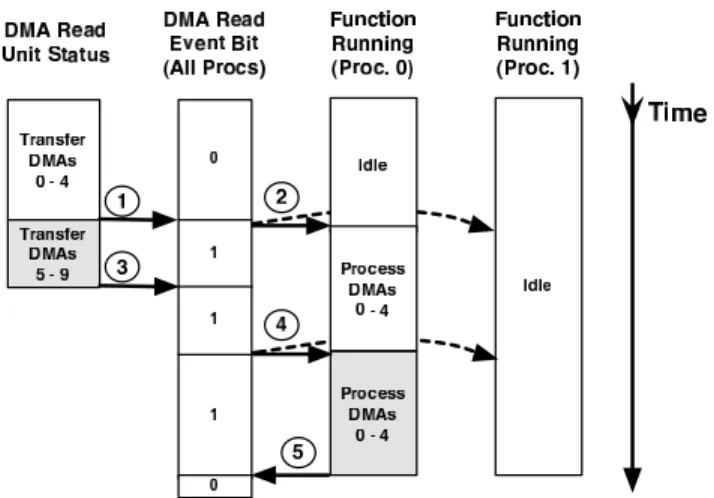
Figure 4 shows how task-level parallel firmware uses an event register to detect a DMA read event and dispatch the appropriate event handler. In step 1, the DMA hardware indicates that some DMAs have completed by setting the global DMA read event bit in every processors’ event regis-ter. In step 2, processor 0 detects this bit becoming set and dispatches the Process DMAs event handler. When DMAs 5 through 9 complete at the DMA read hardware at step 3, the hardware again attempts to set the DMA read event bit, but it is already set. In step 4, processor 0 marks its com-pleted progress as it finishes processing DMAs 0 through 4. Since DMAs 5 through 9 are still outstanding, the DMA read event bit is still set; at this point, either processor 0 or processor 1 could begin executing the Process DMAs han-dler. Finally, in step 5, processor 0 again marks its progress and clears the DMA read event bit, since no more DMAs are outstanding.
Notice that even though DMAs become ready for pro-cessing at step 3 and processor 1 is idle, no processor can begin working on DMAs 5 through 9 until processor 0 fin-ishes working on DMAs 0 through 4. This shortcoming is an artifact of the event register mechanism. The event
regis-Figure 4. Task-level parallel firmware with an event register.
ter only indicates that DMAs are ready, but it does not indi-cate which DMAs are ready. Therefore, so long as a proces-sor is engaged in handling a specific type of event, no other processor can simultaneously handle that same type of event without significant overhead. Specifically, new mechanisms would have to divide events into work units, and the proces-sors and hardware assists would have to collaborate in some manner to decide when to turn event bits on and off.
The straightforward parallelization method depicted in Figure 4 prevents the idle time between steps 3 and 4 from being exposed so long as the handlers are well-balanced across the processors of a given architecture. However, pre-vious studies show that the event handlers of a task-level parallel firmware cannot be balanced across many proces-sors [13].
3.3. Frame-level Parallel Firmware
A key observation of Figure 4 is that task-level paral-lel firmware imposes artificial ordering constraints on frame processing; the processing of DMAs 5 through 9 does not depend on the processing of DMAs 0 through 4. Rather than dividing work according to type and executing differ-ent types in parallel, a frame-level parallel firmware divides work into bundles of work units that need a certain type of processing. Once divided, these work units (described by an event data structure) can be executed in parallel, regardless of the type of processing required. This frame-level paral-lel organization enables higher levels of concurrency but re-quires some additional overhead to build event data struc-tures and maintain frame ordering. The task-processing functions are based on those used in Revision 12.4.13 of Al-teon Websystems’ Tigon-II firmware [3]. However, the code has been extended to make the task processing functions
re-Figure 5. Frame-level parallel firmware using a dis-tributed event queue.
entrant and to apply synchronization to all data shared be-tween different tasks.
Figure 5 illustrates how a frame-level parallel firmware processes the same sequence of DMAs previously illus-trated in Figure 4. As DMAs complete, the DMA hardware updates a pointer that marks its progress. In step 1, pro-cessor 0 inspects this pointer, builds an event structure for DMAs 0 through 4, and executes the Process DMAs han-dler. In step 2, processor 1 notices the progress that indicates DMAs 5 through 9 have completed, builds an event struc-ture for DMAs 5 through 9, and executes the Process DMAs handler. Notice that unlike the task-level parallel firmware in Figure 4, two instances of the Process DMAs handler can run concurrently. As a result, idle time only occurs when there is no other work to be done.
As indicated by Figure 5, a frame-level parallel firmware must inspect several different hardware-maintained pointers to detect events. Furthermore, such a firmware must main-tain a queue of event structures to facilitate software-raised events and retries. Software-raised events signal the need for more processing in another NIC-processing step, while retries are necessary if an event handler temporarily ex-hausts local NIC resources.
A side effect of concurrent event processing is that frames may complete their processing out-of-order with re-spect to their arrival order. However, in-order frame delivery must be ensured to avoid the performance degra-dation associated with out-of-order TCP packet delivery, such as duplicate ACKs and the fast retransmit algo-rithm [1]. To facilitate this, the firmware maintains several status buffers where the intermediate results of network in-terface processing may be written. The firmware’s dis-patch loop inspects the final-stage results in-order for a “done” status and commits all subsequent, consecu-tive frames. The task of committing a frame may not be run concurrently, but committing a frame only
re-CPU 0 Scratch Pad 0 CPU P-1 Scratch Pad S-1 CPU 1 Scratch Pad 1
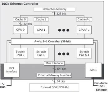
Cache 0 Cache 1 Cache P-1 Instruction Memory External DDR SDRAM 10Gb Ethernet Controller PCI Interface MAC Bus Interface PCI Bus Full-duplex 10Gb Ethernet 32 bits 128 bits 64 bits External Memory Interface
P+4 x S+1 Crossbar (32-bit)
128 bits
Figure 6. 10 Gb/s Ethernet Controller Architecture.
quires a pointer update.
Though the event queue can leverage the proposed archi-tecture’s parallel resources, ensuring in-order frame deliv-ery can impose significant computation and memory over-head. As frames progress from one step of processing to the next, status flags become set that indicate one stage of processing has completed and another is ready to begin. However, operations such as hardware pointer updates re-quire that a consecutive range of frames is ready. To deter-mine if a range is ready and update the appropriate pointer, the firmware processors must synchronize, check for con-secutive set flags, clear the flags, update pointers as neces-sary, and then finally release synchronization. These syn-chronized, looping memory accesses represent a significant source of overhead.
4. 10 Gigabit NIC Architecture
Figure 6 shows the proposed computation and mem-ory architecture. The controller architecture includes par-allel processing cores, a partitioned memory system, and hardware assist units for performing DMA transfers across the host interconnect bus and for performing Ethernet data sends and receives according to the MAC policy. In addi-tion to being solely responsible for all frame data trans-fers, these assist units are also involved with some control data accesses as they share information with the processors about which frame contents are to be or have been trans-ferred.
Each processing core is a single-issue, 5-stage pipelined processor that implements a subset of the MIPS R4000 in-struction set. To allow stores to proceed without stalling the processor, a single store may be buffered in the MEM
stage; loads requiring more than one cycle force the proces-sor to stall. To facilitate the manipulation of the status flags for the event queue mechanism, each processor also imple-ments two atomic read-modify-write operations, setand
update.Settakes an index into a bit array in memory as
an argument and atomically sets only that corresponding bit.
Updateexamines the bit array and looks for consecutive
bits that have been set since the last update, examining at most one aligned 32-bit word.Updateatomically clears the consecutive set bits and returns a pointer indicating the offset at which the last cleared bit was found. Firmware run-ning on these processors can use these instructions to com-municate “done” status information between computation phases and eliminate the synchronization, looping, and flag-update overheads discussed in Section 3.3.
Instructions are stored in a single 128 KB instruc-tion memory which feeds per-processor instrucinstruc-tion caches. Firmware and assist control data is stored in the on-chip scratchpad, which has a capacity of 256 KB and is sepa-rated into S independent banks. The scratchpad is glob-ally visible to all processors and hardware assist units. This provides the necessary communication between the pro-cessors and the assists as the assists read and update de-scriptors about the packets they process. The scratchpad also enables low-latency data sharing between proces-sors.
The processors and each of the four hardware assists connect to the scratchpads through a crossbar as in a dance-hall architecture. There is also a crossbar connection to al-low the processors to connect to the external memory in-terface; the assists access the external memory interface di-rectly. The crossbar is 32 bits wide and allows one trans-action to each scratchpad bank and to the external mem-ory bus interface per cycle with round-robin arbitration for each resource. Accessing any scratchpad bank requires a latency of 2 cycles: one to request and traverse the cross-bar and another to access the memory and return requested data. Hence, the processors must always stall at least one cycle for loads, but store buffering avoids any stalling for stores. If each core had its own private scratchpad, the ac-cess latency could be reduced to a single cycle by elimi-nating the crossbar. However, each core would then be lim-ited to only accessing its local scratchpad or would require a much higher latency to access a remote location.
The processor cores and scratchpad banks operate at the CPU clock frequency, which could reasonably be 200 MHz in an embedded system. At this frequency, if the cores op-erate at 100% efficiency, 4 cores and 2 scratchpad banks could meet the computation and control data bandwidth de-mands described in Section 2.1. To provide sufficient band-width for bidirectional 10 Gb/s data streams, the external memory bus is isolated from the rest of the system since it must operate significantly faster than the CPU cores. It is
not desirable to force the cores to operate faster (thus dis-sipating more power) just so the external memory can pro-vide enough bandwidth for frame data. The PCI interface and MAC unit share a 128-bit bus to access the 64-bit wide external DDR SDRAM. At the same operating frequency, both the bus and the DDR SDRAM have the same peak transfer rate, since the SDRAM can transfer two 64-bit val-ues in a single cycle. If the bus and SDRAM are able to op-erate at 100% efficiency, then they can achieve 40 Gb/s of bandwidth at 312.5 MHz. However, transmit traffic intro-duces significant inefficiency because it requires two trans-fers per frame (header and data), where the header is only 42 bytes. A 64-bit wide GDDR SDRAM operating at 500 MHz provides a peak bandwidth of 64 Gb/s, and is able to sustain 40 Gb/s of bandwidth for network traffic.
Since the PCI bus, the MAC interface, and the exter-nal DDR SDRAM all operate at different clock frequen-cies, there must be four clock domains on the chip. The dif-ferent clock domains are shown with difdif-ferent shadings in Figure 6.
5. Experimental Methodology
The proposed 10 Gigabit Ethernet controller architec-ture is evaluated using Spinach, a library for simulating programmable network interfaces using the Liberty Simu-lation Environment (LSE) [22, 24]. LSE allows a simula-tor to be expressed as a configuration of modules, which can be composed hierarchically at various levels of abstrac-tion and which communicate exclusively through ports. Spinach includes modules applicable to general-purpose programmable systems and modules that are specific to embedded systems and network interfaces. The general-purpose modules include memory controllers, cache con-trollers, memory contents, and bus arbiters. The embedded-systems modules include DMA and MAC assist units, and a network interface test harness. Spinach accurately models multiple clock domains across different hierarchies of mod-ules.
Because Spinach modules use the LSE port abstrac-tion for communicaabstrac-tion, and because ports are evaluated on a cycle-by-cycle basis, Spinach simulators model band-width precisely. Spinach module instances maintain ar-chitectural state and timing information; each instance is evaluated every cycle and determines its behavior accord-ing to user-specified parameters. Since the LSE framework schedules module activation, evaluation, and communica-tion each cycle, the resultant Spinach simulator represents a cycle-accurate, precise model of the system under study. Spinach has been used to accurately model the Tigon-II pro-grammable multiprocessor NIC [24].
The architecture described in Figure 6 is expressed in terms of Spinach modules by instantiating the
correspond-100 125 150 175 200 225 250 275 300 0 2 4 6 8 10 12 14 16 18 20 Core Frequency (MHz)
Total Throughput (Gb/s) Ethernet Limit (Duplex)
8 Processors 6 Processors 4 Processors 2 Processors 1 Processor
Figure 7. Scaling Core Frequency and the Number of Processors.
ing architectural structures, by specifying the port connec-tions between the instances, and by specifying each in-stance’s parameters (latency, arbitration schemes, etc). All inter-module communication follows the paths represented in the figure.
The simulator also models the behavior of the host and the network. The host model emulates the real device driver, while the network model times packet transmission or re-ception based on the Ethernet clock, interframe gaps, and preambles. At the same time, some features of the actual environment are not modeled; in a real system, sends and receives would actually be correlated (e.g., TCP data trans-missions and acknowledgments), but this behavior is not di-rectly exploited by the Ethernet layer and is not captured by the simulation system. Since server I/O interconnect stan-dards are continually evolving (from PCI to X to PCI-Express and beyond), the bandwidth and latency of the I/O interconnect are not modeled. Finally, the proposed archi-tecture is tested under various configurations by simulta-neously sending and receiving Ethernet frames of various sizes.
6. Experimental Results and Discussion
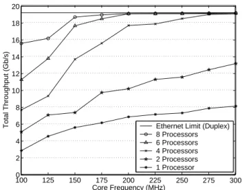
6.1. Parallelism
Figure 7 shows the overall performance of the pro-posed architecture for streams of maximum-sized UDP packets (1472 bytes), which lead to maximum-sized Eth-ernet frames (1518 bytes). The figure shows the achieved UDP throughput as the processor frequency and number of processors in the architecture are varied. All configura-tions use four scratch-pad banks, an 8 KB 2-way set as-sociative instruction cache with 32 byte lines per processor,
Component IPC Contribution
Execution 0.72
Instruction miss stalls 0.01
Load stalls 0.12
Scratchpad conflict stalls 0.05
Pipeline Stalls 0.10
Total 1.00
Table 3. Breakdown of computation bandwidth in instructions per cycle per core.
external SDRAM operating at 500 MHz, and a physical net-work link operating at 10 Gb/s for both transmit and receive traffic. The figure shows that the architectural and software mechanisms enable parallel cores to achieve the peak band-width of the network. At 175 MHz, six cores achieve 96.3% of line rate and eight cores achieve 98.7% of line rate. At 200 MHz, both six and eight cores achieve within 1% of line rate. In contrast, simulation data (not shown in the figure) shows that a single core would have to operate at 800 MHz to achieve line rate.
Table 3 shows a breakdown of the computation resources for six cores operating at 200 MHz each, as that is the small-est number of cores at the lowsmall-est frequency that achieve line rate. Each core has a maximum instruction rate of one instruction per cycle. The cores actually achieve an aver-age of 0.72 instructions per cycle because of instruction misses, scratch pad latency, and pipeline hazards. Instruc-tion misses only account for 0.01 lost instrucInstruc-tions per cycle. This shows that the small instruction caches are extremely effective at capturing code locality even though tasks mi-grate from core to core. The six cores combined execute 142.8 million scratchpad loads per second and 107.8 mil-lion scratch pad stores per second. Recall from Section 4 that a scratchpad access takes a minimum of two cycles, but that each core may buffer up to one store. If there are no conflicts, then a scratchpad load forces a single cycle pipeline load stall, and a scratchpad store causes no stalls. So, scratchpad loads account for 0.12 lost instructions per cycle. While splitting the MEM stage into multiple stages could eliminate some of these stalls, 50% of all loads in this firmware cause load-to-use dependences that always incur a stall for the dependent instruction and thus would not ben-efit from lengthening the pipeline. In addition to scratchpad load stalls, scratchpad bank conflicts account for another 0.05 lost instructions per cycle. The remaining 0.10 instruc-tion issue slots per cycle are lost to pipeline stalls due to hazards. Cycles are lost to stalls in this pipeline when the re-sult of a load is used by the subsequent instruction and when the branch condition is not computed early enough. Instruc-tions that are annulled by statically mispredicted branches are also included in this category. These lost cycles cannot be avoided without complicating the pipeline. While many solutions exist, they would all increase the power and area
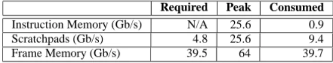
Required Peak Consumed
Instruction Memory (Gb/s) N/A 25.6 0.9 Scratchpads (Gb/s) 4.8 25.6 9.4 Frame Memory (Gb/s) 39.5 64 39.7
Table 4. Bandwidth consumed by the six 200 MHz core configuration.
of the core, which is not desirable in such an embedded sys-tem.
In all, these very simple pipelined cores are able to achieve a respectable level of sustained IPC. In fact, they sustain 83% of the theoretical peak IPC of in-order cores with no branch prediction, as presented in Section 2.2. As the table shows, a significant amount of the difference arises from memory stalls.
6.2. Memory Efficiency
Table 4 shows the amount of instruction and data band-width that is needed to saturate the Ethernet link. The ta-ble also includes the minimum requirements to achieve line rate, as discussed in Section 2.1. For reference, the table shows the peak rates possible on the six core architecture, which clearly indicates that memory bandwidth must be overprovisioned in order to achieve line rate. For example, instruction misses rarely occur because of the firmware’s small code footprint. The 128-bit interface to the instruc-tion memory is available to fill cache lines as needed, but it is unused almost 97% of the time.
Table 4 also highlights the data bandwidth consumed by this architecture. The processing cores make 250.6 million accesses to the scratchpad per second, and the hardware as-sists make an additional 41.7 million accesses per second. This results in 9.4 Gb/s of scratchpad bandwidth. As dis-cussed previously, these scratchpad accesses and the asso-ciated conflicts already account for 17% of the lost compu-tation resources. Furthermore, the hardware assists are also sensitive to the latency of scratchpad accesses. Because in-creased latency (in the form of inin-creased bank conflicts) would reduce performance, the aggregate bank bandwidth must be overprovisioned to ensure low latency.
The external SDRAM is used only for frame data. Both incoming and outgoing data is stored once and retrieved once in this memory. This leads to 39.7 Gb/s of consumed bandwidth. This is higher than the strictly required band-width only because of misaligned accesses. Frames fre-quently are not stored in the transmit and receive buffers such that they start and/or end on even 8-byte boundaries. Even though the unused bytes are not used when read and are masked off when written, this is lost SDRAM bandwidth that cannot be recovered, so it is counted in the totals. The high latency of this memory (up to 27 cycles when there are SDRAM bank conflicts) does not affect performance
Function Ideal Instructions per Packet Memory Accesses per Packet
Software-only RMW-enhanced Ideal Software-only RMW-enhanced
Fetch Send BD 24.5 39.1 38.5 10.6 14.4 14.4
Send Frame 256.9 317.3 311.5 90.0 102.5 92.4
Send Dispatch and Ordering - 292.1 141.7 - 94.0 32.9
Send Locking - 2.6 10.6 - 0.9 2.7
Fetch Receive BD 12.1 12.4 12.2 4.1 5.3 4.2
Receive Frame 241 292.1 335.5 80.8 135.4 126.2
Receive Dispatch and Ordering - 202.5 140.7 - 66.2 42.9
Receive Locking - 20.5 34.4 - 5.1 8.6
Table 5. Execution profiles comparing frame-ordering methods.
adversely. In contrast to the scratchpads, bandwidth is far more important than latency for frame data. This bandwidth exceeds the capabilities of the scratchpads, further validat-ing the partitioned memory architecture.
6.3. Firmware
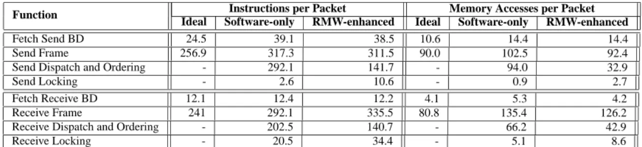
Table 5 highlights the effectiveness of the proposedset
andupdateRMW instructions as described in Section 4.
The table shows the execution profile of six cores process-ing maximum-sized frames. The RMW-enhanced configu-ration uses the atomic set and update RMW instruc-tions to manage frame ordering and hardware pointer up-dates, but the software-only approach uses basic lock-based synchronization to manage status flags. The ideal require-ments established in Table 1 are provided as reference. The addition of the RMW instructions reduces the per-frame instruction ordering and dispatch overheads by 51.5% for sent frames and by 30.8% for received frames. RMW in-structions replace multiple looping memory accesses in the firmware’s dispatch and ordering functions. In the order-ing and dispatch functions, these replacements reduce the number of memory accesses by 65.0% and 35.2% for sent and received frames, respectively. Note, however, that con-tention among the remaining firmware locks increases. This problem is particularly troublesome for a lock in the receive path, which leads to imbalance among the receive functions. This imbalance causes the per-frame instructions executed for receive functions to increase slightly.
The reduction in per-frame processing requirements en-ables a 6-processor NIC configuration to reduce its proces-sor and scratchpad frequency from 200 MHz to 166 MHz. Table 6 shows the per-packet cycle requirements for each portion of NIC processing for the 200 MHz software-only and 166 MHz RMW-enhanced configurations. Both con-figurations achieve line rate for full-duplex streams of maximum-sized packets. The RMW-enhanced configu-ration reduces send cycles by 28.4% and receive cycles by 4.7%. The firmware’s dynamic task-queue organiza-tion exploits these reducorganiza-tions to enable a clock frequency reduction of 17%.
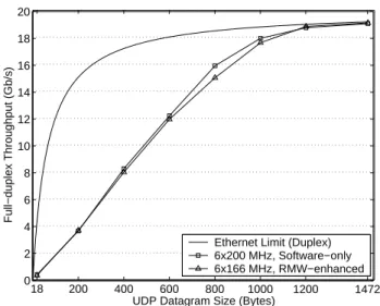
Finally, Figure 8 shows the performance of both con-figurations for streams of various frame sizes. The
maxi-mum full-duplex Ethernet bandwidth for each frame size is shown as reference; because per-frame overheads are con-stant, payload data throughput decreases as frame sizes de-crease. The figure shows that both configurations scale sim-ilarly across frame sizes. As frame sizes reduce, however, the increased frame rates cause both configurations to be-come limited by processing resources. Both configurations saturate at a rate of about 2.2 million frames per second, though the RMW-enhanced configuration’s peak is slightly lower due to event-function imbalances caused by lock con-tention. This lower peak frame rate leads to the performance gap at 800-byte UDP packets. As the packet size decreases from 800 bytes, both configurations become saturated at their peak frame rates, and the decrease in packet size pro-portionally decreases the gap in performance. Because the RMW-enhanced system maintains competitive performance across frame sizes, it provides the opportunity to reduce power consumption by using lower clock frequencies.
7. Related Work
Intel has prototyped an accelerator for inbound TCP pro-cessing on a 10 Gigabit Ethernet link [10]. However, the de-scribed system only has a programmable header process-ing engine with a special-purpose instruction-set; it does not provide any solutions for sending TCP data, memory bandwidth requirements, payload transfer, or DMA support to transfer data between the host and the system. Conse-quently, this is a valuable component of a TCP-offloading network interface but is not a complete solution. The in-bound processing engine alone requires 6.39 W for 10 Gb/s line speed, running at a clock rate of 5 GHz. The system de-scribed in this paper instead uses multiple low-frequency cores to provide the required performance without consum-ing excessive power.
Several companies have also announced 10 Giga-bit Ethernet NIC products, both programmable and non-programmable. However, few of these NICs are currently available to the public, and very little concrete informa-tion has been made available about their architectures. Hurwitz and Feng performed an evaluation of the In-tel PRO/10GbE LR NIC, which does not support TCP offloading, in commodity systems [11]. Their study
re-Function Software-only RMW-enhanced
Fetch Send BD 62.4 56.3
Send Frame 427.4 407.9
Send Dispatch and Ordering 389.5 159.8
Send Locking 6.7 19.4
Send Total 886.0 643.4
Fetch Receive BD 17.5 16.1
Receive Frame 401.4 438.8
Receive Dispatch and Ordering 281.9 192.9
Receive Locking 44.2 62.5
Receive Total 745.0 710.3
Table 6. Cycles spent in each function per packet for each frame-ordering method.
ports the achievable bandwidth between systems us-ing these NICs under varyus-ing circumstances. However, the lack of both architectural information and an isolated per-formance evaluation prevents direct comparisons to the architecture proposed here.
In contrast, multi-core network processors have been widely investigated for router line card applications [6, 7, 8, 14]. Two primary packet processing parallelization mod-els exist for such systems: threaded and pipelined. In the threaded model, a different hardware context is used for each packet being processed [8]. In the pipelined model, the cores support task-level concurrency with packets flow-ing from one core to the next durflow-ing processflow-ing [7]. Both types of systems often use multithreaded cores to tolerate latencies. However, the latencies they tolerate are for ac-cesses to their local memories and off-chip SDRAMs as they perform tasks such as table lookups. These systems are not directly applicable to server network interfaces be-cause frame processing requires the network interface to access the host’s memory through DMA. The latencies of such DMA accesses are significantly higher because they must traverse the local interconnect to get to memory rather than accessing memory directly connected to the proces-sors. Furthermore, arbitration, addressing, and stalls on the local interconnect incur additional latency. Consequently, a network processor using either the threaded or pipelined model would require an excessive number of contexts to tol-erate DMA latencies; for example, the proposed 10 Gigabit NIC in this paper has several hundred outstanding frames in various stages of processing at any given time.
Additionally, the longer latencies of DMAs would likely lead to imbalances among the stages in a pipelined system. For example, Mackenzie et al. found such mismatches when using the Intel IXP network processor for network interface processing [15]. Their system used an Intel IXP 1200 op-erating at 232 MHz and used about 40% of its processing power to achieve 400 Mb/s of peak throughput, suggest-ing a peak throughput of 1 Gb/s. Though the IXP 1200 fea-tures six multithreaded cores and a StrongARM processor, the much older Tigon-II programmable NIC achieves
Giga-18 200 400 600 800 1000 1200 1472 0 2 4 6 8 10 12 14 16 18 20
UDP Datagram Size (Bytes)
Full−duplex Throughput (Gb/s)
Ethernet Limit (Duplex) 6x200 MHz, Software−only 6x166 MHz, RMW−enhanced
Figure 8. Full-duplex throughput for various UDP datagram sizes.
bit speeds with only two simple 88 MHz cores. This sug-gests that network processor-based solutions are not as ef-ficient at handling a network interface workload as a sys-tem designed explicitly as a network interface controller. Finally, the multi-gigahertz cores found in router line cards dissipate far more power than is allowed of a PCI card in a network server.
The proposed network interface architecture exploits the principle that parallel processing cores provide higher per-formance at lower complexity than either a high-frequency or wide-issue core. Similar observations have been made before in the context of general-purpose processors through research on multiscalar processors, trace processors, and chip multiprocessors [9, 19, 21]. These schemes also fa-cilitate speculative code parallelization. In contrast, the ar-chitecture proposed here targets a special-purpose workload that is inherently parallelizable and focuses instead on the memory system and software structure required to exploit that parallelism across a large number of processing cores.
8. Conclusions
This paper proposes and evaluates an architecture for an efficient programmable 10 Gigabit Ethernet controller. The processing characteristics and power budgets of net-work interfaces prohibit the use of high clock frequencies, wide-issue superscalar processors, and complex cache hi-erarchies. Furthermore, network interfaces must handle a large volume of frame data, provide low-latency access to frame metadata, and meet the high computational require-ments of frame processing. The proposed architecture effi-ciently achieves the required performance through a com-bination of a heterogeneous and partitioned memory
sys-tem, an event-queue mechanism, parallel scalar processors, and decoupled clock domains. A controller operating at 166 MHz with 6 simple pipelined cores, private 8 KB 2-way set associative instruction caches, a 4-way banked scratch-pad, and 64-bit 500 MHz GDDR SDRAM can achieve 99% of theoretical peak throughput of 10 Gb/s full-duplex Ether-net bandwidth on a bidirectional stream of maximum-sized Ethernet frames.
Ethernet processing has substantial architectural and software challenges related to the efficient manage-ment and transfer of large volumes of frame data and metadata. The use of a programmable interface with sub-stantial computational and memory resources, however, is motivated primarily by the ability to extend beyond Ether-net processing. Proposed uses for programmable Ether-network interfaces include full and partial TCP offload, mes-sage passing, iSCSI, file caching on the network interface, and intrusion detection [4, 5, 10, 12, 16, 18, 20]. The pro-posed architecture provides a solid base for implementing such services.
References
[1] M. Allman, V. Paxson, and W. Stevens. TCP Congestion Control. IETF RFC 2581, Apr. 1999.
[2] Alteon Networks. Tigon/PCI Ethernet Controller, Aug.
1997. Revision 1.04.
[3] Alteon WebSystems. Gigabit Ethernet/PCI Network In-terface Card: Host/NIC Software InIn-terface Definition, July
1999. Revision 12.4.13.
[4] H. Bilic, Y. Birk, I. Chirashnya, and Z. Machulsky. Deferred Segmentation for Wire-Speed Transmission of Large TCP Frames over Standard GbE Networks. In Hot Interconnects
IX, pages 81–85, Aug. 2001.
[5] G. R. Ganger, G. Economou, and S. M. Bielski. Find-ing and ContainFind-ing Enemies Within the Walls with Self-securing Network Interfaces. Technical Report CMU-CS-03-109, Carnegie Mellon School of Computer Science, Jan. 2003.
[6] P. N. Glaskowsky. Intel Beefs Up Networking Line.
Micro-processor Report, Mar. 2002.
[7] L. Gwennap. Cisco Rolls its Own NPU. Microprocessor
Re-port, Nov. 2000.
[8] T. R. Halfhill. Sitera Samples its First NPU. Microprocessor
Report, May 2000.
[9] L. Hammond, B. A. Nayfeh, and K. Olukotun. A Single-Chip Multiprocessor. IEEE Computer, Sept. 1997.
[10] Y. Hoskote, B. A. Bloechel, G. E. Dermer, V. Erraguntla, D. Finan, J. Howard, D. Klowden, S. G. Narendra, G. Ruhl, J. W. Tschanz, S. Vangal, V. Veeramachaneni, H. Wilson, J. Xu, and N. Borkar. A TCP Offload Accelerator for 10 Gb/s Ethernet in 90-nm CMOS. IEEE Journal of Solid-State
Circuits, 38(11):1866–1875, Nov. 2003.
[11] J. Hurwitz and W. Feng. End-to-End Performance of 10-Gigabit Ethernet on Commodity Systems. IEEE Micro,
Jan./Feb. 2004.
[12] H. Kim, V. S. Pai, and S. Rixner. Improving Web Server Throughput with Network Interface Data Caching. In
Pro-ceedings of the Tenth International Conference on Architec-tural Support for Programming Languages and Operating Systems, pages 239–250, October 2002.
[13] H. Kim, V. S. Pai, and S. Rixner. Exploiting Task-Level Con-currency in a Programmable Network Interface. In
Proceed-ings of the ACM SIGPLAN Symposium on Principles and Practice of Parallel Programming, June 2003.
[14] K. Krewell. Rainier Leads PowerNP Family.
Microproces-sor Report, Jan. 2001.
[15] K. Mackenzie, W. Shi, A. McDonald, and I. Ganev. An In-tel IXP1200-based Network Interface. In Proceedings of the
2003 Annual Workshop on Novel Uses of Systems Area Net-works (SAN-2), Feb. 2003.
[16] K. Z. Meth and J. Satran. Design of the iSCSI Protocol. In
Proceedings of the 20th IEEE Conference on Mass Storage Systems and Technologies, Apr. 2003.
[17] Micron. 256Mb: x32 GDDR3 SDRAM MT44H8M32 data sheet, June 2003.
[18] Microsoft Corporation. Windows Network Task Offload. In
Microsoft Windows Platform Development, Dec. 2001.
[19] E. Rotenberg, Q. Jacobson, Y. Sazeides, and J. Smith. Trace Processors. In Proceedings of the 30th Annual International
Symposium on Microarchitecture, pages 138–148,
Decem-ber 1997.
[20] P. Shivam, P. Wyckoff, and D. Panda. Can User Level Pro-tocols Take Advantage of Multi-CPU NICs? In Proceedings
of IPDPS2002, Apr. 2002.
[21] G. S. Sohi, S. E. Breach, and T. N. Vijaykumar. Multiscalar Processors. In Proceedings of the 22nd Annual International
Symposium on Comput er Architecture, pages 414–425, June
1995.
[22] M. Vachharajani, N. Vachharajani, D. A. Penry, J. A. Blome, and D. I. August. Microarchitectural Exploration with Lib-erty. In Proceedings of the 35th Annual International
Sympo-sium on Microarchitecture, pages 271–282, November 2002.
[23] M. A. Vega Rodr´ıguez, J. M. S´anchez P´erez, R. Mart´ın de la Monta˜na, and F. A. Zarallo Gallardo. Simulation of Cache Memory Systems on Symmetric Multiprocessors with Edu-cational Purposes. In Proceedings of the First International
Congress in Quality and in Technical Education Innovation,
volume 3, pages 47–59, Sept. 2000.
[24] P. Willmann, M. Brogioli, and V. S. Pai. Spinach: A Liberty-based Simulator for Programmable Network Interface Ar-chitectures. In Proceedings of the ACM SIGPLAN/SIGBED
2004 Conference on Languages, Compilers, and Tools for Embedded Systems, pages 20–29. ACM Press, July 2004.