A high Step-up DC-DC Converter employs Cascading
Cockcroft-Walton Voltage Multiplier by omitting Step-up Transformer
1A.Subrahmanyam,2A.Tejasri
M.Tech(Research scholar),Assistant Professor,Dept. of EEE in Godavari Institute of Engineering & Technology (GIET),Rajahmundry(A.P),INDIA.
E.mail:[email protected],[email protected]
Abstract: In my paper possess a high voltage gain and devoid of using Step up transformer through a high step-up DC-DC converter based on Cockcroft-Walton (CW) voltage multiplier. Here the input was in low to DC voltage is boost up with the help of boost inductor in DC-DC converter. The n-number of stages CW-voltage multiplier is applying input as low to AC voltage to high output DC voltage. This afford gets a continuous input current with low ripple, high voltage gain, reduced switching losses, low voltage stress on the switches, diodes & capacitors and also improving efficiency of the converter. In my paper, strategic controlled steps retain two independent frequencies, one of which operates at high frequency to optimized size of the inductor while the other one operates at comparatively low in frequency according to the desired output voltage ripple. Finally this converter is authorized by simulation and experimental result is designed.
Key words: CW-Cockcroft-Walton, Boost inductor, Output voltage ripple.
I. Introduction
The conventional boost DC-DC converter can provide a very high voltage gain by using an extreme high duty cycle. The step-up dc-dc converters have been proposed to obtain high voltage ratios without extreme high duty cycle by using isolated transformers or coupled inductors. Among these high step-up dc-dc converters, voltage-fed type sustains high input current ripple. Thus, providing low input current ripple and high voltage ratio, current-fed converters are generally superior to their counterparts. However, in order to achieve high voltage gain,the leakage inductance of the
transformer is relatively increased due to the high number of winding turns. Consequently, th switch is burdened with high voltage spikes across the switch at the turn-off instant. Thus, higher voltage-rating switches are required.The current fed converters are providing low input current ripple and high voltage ratio. Modified current-fed converters integrated with step-up transformers or coupled-inductors which focused on improving efficiency and reducing voltage stress, were presented to achieve high voltage gain without extreme high duty cycle.
The design of high-frequency transformers, coupled inductors or resonant components for these converters are relatively complex compared with the conventional boost DC converter. The step-up DC-DC converters without step-up transformers and coupled inductors were presented. By cascading diode-capacitor or diode-inductor modules, these kinds of DC-DC converters provide not only high voltage gain but also simple and robust structures.
The conventional Cockcroft-Walton voltage multiplier is very popular among high voltage DC applications. Replacing the step-up transformer with the boost type structure, the proposed converter provides higher voltage ratio than that of the conventional CW voltage multiplier.
II. Steady state Analysis
operating frequencies of Sm1 and Sc1 are defined as fsm and fsc, respectively. For convenience, fsm is denoted as modulation frequency and fsc is denoted as alternating frequency. Theoretically, these two frequencies should be as high as possible, so that smaller inductor and capacitors can be used in this circuit. In this paper, fsm is set much higher than fsc, and the output voltage is regulated by controlling the duty cycle of Sm1 and Sm2, while the output voltage ripple can be adjusted by fsc. As shown in Fig.1, the well-known CW voltage multiplier is constructed by a cascade of stages with each stage containing two capacitors and two diodes. In an n-stage CW voltage multiplier, there are N (=2n) capacitors and N diodes.
Fig.1 Proposed converter with n-stage CW voltage multiplier
III. Mathematical Model
As shown in Fig.1 the proposed converter is an integration of a boost converter with a CW voltage multiplier. For analysis, the equivalent circuit of the proposed converter can be divided into source-side and load-side parts. For the source-side part, the conducting states dsc and dsm are defined in Table I, where strategy I does not include safe commutation and strategy II includes safe commutation. According to the conducting states dsc and dsm, the differential equation of the inductor current is given by
where Vin is the input voltage, iL is the input current, and vγ is the terminal voltage of the CW voltage multiplier. Assuming that the converter operates in CCM, the current iγ flowing into the CW voltage multiplier depends on dsm and dsc and can be expressed as
where the currentiγcan be deemed a pulse-form current source. In, the mathematical model of an n-stage CW voltage multiplier was discussed and simplified the equivalent circuit, which was convenient for simulation work.
Circuit operation principle
In order to simplify the analysis of
circuit
operation, the proposed converter
with a three-stage CW voltage multiplier, as
shown in Fig3.1. is used Before analyzing,
some assumptions are made as follows.
1) All of the circuit elements are ideal, and
there is no power loss in the system.
reasonable load condition. Thus, the
voltages across
3) all capacitors are equal, except the first
capacitor whose voltage is one half of the
others.
4) 3) The proposed converter is operating in
CCM and in the steady-state condition.
5) 4) When the inductor transfers the storage
energy to the CW circuit, only one of the
diodes in the CW
circuit will be
conducted.
6)
5) Some safe commutation states are
ignored.
Fig.3.1 Converter with three-stage CW
voltage multiplier
According to the second assumption, each
capacitor voltage in the CW voltage multiplier
can be defined as
where vck is the voltage of the kth capacitor
and Vc is the steady-state voltage of vc2
−vcN .
For an n-stage CW voltage multiplier, the
output voltage is equal to the total voltage of
all even capacitors, which can be expressed as
Substituting (16) into (15), each capacitor
voltage in an n-stage CW voltage multiplier
can
also
be
expressed
as
where Vo is the steady-state voltage of the
output load side.
Fig.3.2 Ideal waveforms of the proposed
converter in CCM.
states III, IV-A, IV-B, and IV-C. According to
Fig. 3.3, the circuit operation principle of the
proposed converter is illustrated in detail as
follows.
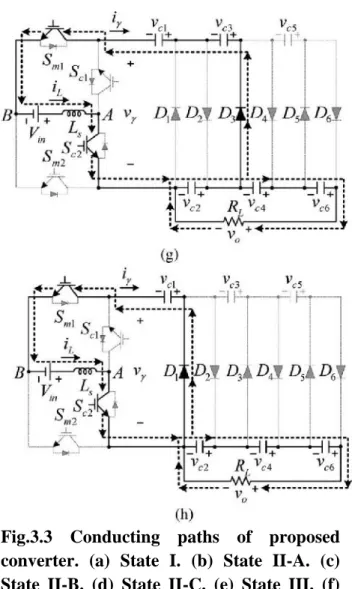
1) State I: Sm1 and Sc1 are turned on, and
Sm2, Sc2, and all CW diodes are turned off, as
shown in Fig.3.3(a). The boost inductor is
charged by the input dc source, the evengroup
capacitors C6, C4, and C2 supply the load, and
the odd-group capacitors C5, C3, and C1 are
floating.
source transfer energy to the CW voltage
multiplier through different even diodes, as
shown in Fig.3.3 (b)
–
(d). In Fig.3.3(b), state
II-A, D6 is conducting; thus, the even-group
capacitors C6, C4, and C2 are charged, and the
odd-group capacitors C5, C3, and C1 are
discharged by
iγ
. In Fig.3.3 (c), state II-B, D4
is conducting. Thus, C4 and C2 are charged,
C3 and C1 are discharged by
iγ
, C6 supplies
load current, and C5 is floating. In Fig.3.3 (d),
state II-C, D2 is conducting. Thus, C2 is
charged, C1 is discharged by
iγ
, C6 and C4
supply load current, and C5 and C3 are
floating.
3) State III: Sm2 and Sc2 are turned on, and
Sm1, Sc1, and all CW diodes are turned off, as
shown in Fig.3.3(e). The boost inductor is
charged by the input dc source, the even group
capacitors C6, C4, and C2 supply the load, and
the odd-group capacitors C5, C3, and C1 are
floating.
4) State IV: Sm1 and Sc2 are turned on, Sm2
and Sc1 are turned off, and the current
iγ
is
negative. The boost inductor and input dc
source transfer energy to the CW voltage
multiplier through different odd diodes, as
shown in Fig.3.3 (f)
–
(h). In Fig. 3.3 (f), state
IV-A, D5 is conducting.
Fig.3.3
Conducting
paths of proposed
converter. (a) State I. (b) State II-A. (c)
State II-B. (d) State II-C. (e) State III. (f)
State IV-A. (g) State IV-B. (h) State IV-C
Design Considerations Of Proposed Converter:
In this, the voltage and current stresses on each capacitor, switch, and diode will be considered. Moreover, the values of inductor and capacitors Fig.4 (a-h) discussed as well.
Design Considerations:
i. Capacitor Voltage Stress
ii. Switch Voltage and Current Stresses iii. Diode Voltage and Current Stresses iv. Input Inductance
v. Capacitance of CW Voltage Multiplier vi. Number of Major Components
Fig. 5 Voltage gain versus duty cycle for the proposed converter under n = 1−8 and the classic boost dc-dc
converter
TABLE II
Comparison of proposed converter and other converters
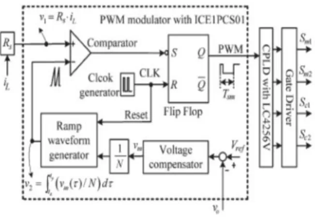
Control Strategy Of Proposed Converter:
discontinuous inductor current will cause voltage spike and damage the switching elements. However, the switching strategy, on the four switches of the proposed converter is not including safe commutation technique. Therefore, another switching strategy including safe commutation technique under the same output function is used in the control strategy of the proposed converter to avoid open circuit of the inductor.
Fig. 6 Control strategy of proposed converter including safe commutation technique.
IV. Simulation Results
Fig. 7 High Step-up DC-DC Converter using Cascaded Cockcroft-Walton Voltage Multiplier
Fig.8 Control Strategy Of Proposed Converter
Fig.9
Some selected waveforms for simulation
at full-load P o = 200 W andV in =48V of
Sc1,Sm1,Vo,Il
Fig.10. Some selected waveforms for simulation
at full-load P o = 200 W and V in =48V of
Sc1,Sm1,Vr,I r
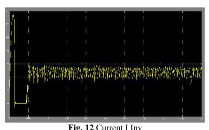
Fig. 12 Current I Inv
V. Conclusion
In my paper, got a high voltage gain and devoid of using Step up transformer through a high step-up DC-DC converter based on Cockcroft-Walton (CW) voltage multiplier. Since the voltage stress on the active switches, diodes, and capacitors is not affected by the number of cascaded stages, power components with same voltage ratings can be selected. The mathematical modeling, circuit operation, design considerations, and control strategy were discussed. The control strategy of the proposed converter can be easily implemented with a commercial average-current-control and continuous current mode with adding a programmed. The proposed control strategy employs two independent frequencies, one of which operates at high frequency to minimize the size of the inductor, while the other one operates at relatively low frequency according to the desired output voltage ripple. Finally, the simulation and experimental results proved the validity of theoretical analysis and the feasibility of the proposed converter. In future work, the influence of loading on the output voltage of the proposed converter will be derived for completing the steady-state analysis. Thus the design, simulation and analysis of proposed DC-DC boost converter with seven-stage Cockcroft Walton voltage multiplier was done.
References
[1] C.-M. Young, M.-H. Chen, T.-A. Chang, and C.-C.
Ko, “Cascade Cockcroft–Walton Voltage Multiplier Applied to Transformerless High Step-Up DC–DC
Converter” IEEE Transactions On Industrial
Electronics, Vol. 60, No. 2, Feb. 2013.
converter for fuel cells to utility interface,” IEEE Trans.
Ind. Electron., vol. 59, no. 1, pp. 473–485, Jan. 2012.
[3] C. S. Leu, P. Y. Huang, and M. H. Li, “A novel
dual-inductor boost converter with ripple cancellation for high-voltage-gain applications,” IEEE Trans. Ind.
Electron., vol. 58, no. 4, pp. 1268–1273, Apr. 2011. [4] W. Li and X. He, “Review of non isolated high -step-up dc/dc converters in photovoltaic grid-connected
applications,” IEEE Trans. Ind. Electron., vol. 58, no. 4,
pp. 1239–1250, Apr. 2011.
[5] I. C. Kobougias and E. C. Tatakis, “Optimal design
of a half-wave Cockcroft–Walton voltage multiplier
with minimum total capacitance,” IEEE Trans. Power
Electron., vol. 25, no. 9, pp. 2460–2468, Sep. 2010. [6] L. S. Yang, T. J. Liang, and J. F. Chen,
“Transformer less dc-dc converters with high step-up
voltage gain,” IEEE Trans. Ind. Electron., vol. 56, no. 8,
pp. 3144–3152, Aug. 2009.
[7] C. M. Young and M. H. Chen, “A novel single -phase ac to high voltage dc converter based on Cockcroft–Walton cascade rectifier,” in Proc. IEEE
PEDS, 2009, pp. 822–826.
[8] S. S. Lee, S. W. Rhee, and G. W. Moon, “Coupled
inductor incorporated boost half-bridge converter with
wide ZVS operation range,” IEEE Trans. Ind. Electron.,
vol. 56, no. 7, pp. 2505–2512, Jul. 2009.
[9] J. M. Kwon, E. H. Kim, B. H. Kwon, and K. H.
Nam, “High-efficiency fuel cell power conditioning
system with input current ripple reduction,” IEEE
Trans. Ind. Electron., vol. 56, no. 3, pp. 826–834, Mar. 2009.
[10] B. Axelrod, Y. Berkovich, and A. Ioinovici,
“Switched-capacitor/switched-inductor structures for getting transformer less hybrid dc-dc PWMconverters,”
IEEE Trans. Circuits Syst. I, Reg. Papers, vol. 55, no. 2, pp. 687–696, Mar. 2008.
[11] Y. Berkovich, B. Axelrod, and A. Shenkman, “A
novel diode-capacitor voltage multiplier for increasing
the voltage of photovoltaic cells,” in Proc. IEEE COMPEL, Zurich, Switzerland, Aug. 2008, pp. 1–5. [12] M. Prudente, L. L. Pfitscher, G. Emmendoerfer, E.
F. Romaneli, and R. Gules, “Voltage multiplier cells applied to non-isolated dc-dc converters,” IEEE Trans.