A New Multilevel Inverter Topology For High Step Up DC-DC
Converter
G Aruna*1 D Srinivas Rao2
M.Tech Student, Department of EEE, KIET, Kakinada, India.1 Asst. Professor, Department of EEE, KIET, Kakinada, India.2
Abstract-High step up proportion dc–dc converters with megawatt evaluations are of enthusiasm for wind turbine interfaces and high-voltage direct current frameworks. This paper introduces a secluded multilevel dc–dc converter in view of the standard boost converter topology yet with the typical single switches supplanted by various capacitor-cinched sub modules. The converter is worked in resounding mode with reverberation between sub module capacitors and the arm inductor. A phase-shifted switching course of action is connected with the end goal that there is a consistent number, i.e., N, of sub modules supporting the high voltage at once. In this operation mode, the progression up proportion is reliant on the quantity of sub modules and the inductor charging proportion. The converter shows versatility without utilizing a transformer and is equipped for bidirectional power stream. This venture is reached out to next sub module for expanding working scope of the converter. The outcomes checked through MATLAB/SIMULINK condition.
Index Terms—DC transformer, high-voltage coordinate current (HVDC) converters, secluded multilevel converters (MMCs), full change, venture up dc–dc transformation.
I.INTRODUCTION
The improvement of electric and half and half electric vehicles will offer numerous new open doors and difficulties to the power hardware industry, particularly in the advancement of the primary footing engine drive . Numerous present and future plans will join the utilization of enlistment engines as the essential hotspot for footing in electric vehicles. Plans for overwhelming obligation trucks and numerous military battle vehicles that have vast electric drives will require propelled control electronic inverters to meet the powerful requests (>250 kw) required of them. Advancement of electric drive trains for these expansive vehicles will bring about expanded fuel % betroth, bring down emanations, and likely better vehicle execution (speeding up and braking). Multilevel inverters are exceptionally suited for this
application as a result of the high VA appraisals conceivable with these inverters.
Where produced air conditioning voltage is accessible, for example, from an alternator or air conditioning generator, a consecutive diode-clasped converter can change over this source to variable recurrence air conditioning voltage for the determined engine. For electric vehicles (EVS), a fell H-spans inverter can be utilized to drive the footing engine from an arrangement of batteries or energy units. Some conventional 2-level high-recurrence beat width balance (PWM) inverters for car drives can have issues related with their high voltage change rates (dV/dt), which creates a typical mode voltage over the engine windings.
High recurrence exchanging can fuel the issue on account of the various circumstances this basic mode voltage is urged the engine each cycle. PWM controlled inverters likewise require a more noteworthy measure of warmth evacuation in light of the extra exchanging misfortunes. Multilevel inverters take care of these issues on the grounds that their individual gadgets have a much lower dV/dt per exchanging, and they work at high efficiencies since they can switch at a lower recurrence than PWM-controlled inverters.
lines, the aggregate volume of capacitors required is very high. Summed up multilevel converters can be utilized for venture up dc–dc transformation [8], [9], yet the topology brings about an extensive size when the progression proportion is high. Different topologies, for example, input-parallel yield arrangement (IPOS) converters [10] and exchanged capacitor converters have been proposed and created for venture up dc–dc transformation [11]–
[12].
The IPOS converters utilize full sub modules to accomplish high-control change and effectiveness , yet the primary weakness is the prerequisite of countless transformers, which have high potential contrasts between the windings. Exchanged capacitor converters with arrangement parallel topologies are liable to incremental voltage stretch either on the module switch or on the module capacitor. The most elevated voltage stress is near the yield (high-side) dc voltage. The exchanged capacitor converters are additionally subject to high charge misfortunes and overshoot streams. This issue can be moderated by driving metal–oxide–semiconductor field-impact transistors (MOSFETs) with high exchanging recurrence. Along these lines, exchanged capacitor converters are just utilized under a low-voltage condition. A power-gadgets based Cockcroft–Walton multiplier has been shown in . This is a light and shoddy answer for high-voltage dc tests when just unidirectional stride up transformation is required. A bidirectional medium voltage "stepping stool"- molded dc–dc converter is proposed in , which can accomplish a high stride proportion. The preferred standpoint is that the converter does not require synchronization of exchanging between sub modules. Be that as it may, the present evaluations in various sub modules are not the same, and the inductor streams near the low-voltage side are high. In medium-and high-voltage applications, MMCs utilized for dc–dc transformation are developing innovations [5], [12]. These converters depend on regular MMCs . MMCs more often than not require an entangled adjusting control plan to keep up the voltage levels. In any case, they give more than two levels and great waveform quality. Cells with blame can likewise be skirted while keeping the framework operational. High seclusion and excess are the principle points of interest of MMCs. As of recently, there has been no immediate and straightforward answer for substantial stride up proportion dc–dc transformation utilizing the MMC approach. This paper shows another topology and control plan of a secluded multilevel bidirectional dc–dc converter with high stride up proportion. It depends on the regular lift converter with gatherings of sub modules put in both the diode and switch positions. The proposed converter can accomplish a high stride proportion. Stage moved heartbeat width
successful working recurrence for a given sub module exchanging recurrence. The proposed converter is bidirectional and appropriate for low-control dc–dc applications as it has the component of measured quality, effortlessness, and adaptability. The design of the circuit and its operation standard are displayed.
II.BIDIRECTIONAL MODULAR
MULTILEVEL DC–DC CONVERTERS
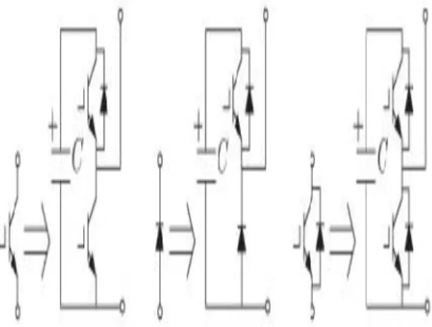
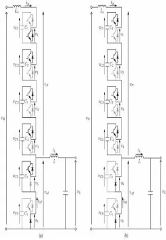
In converting a simple standard s witched-mode circuit t o a modular multilevel format, a variety of capacitor- clamped sub modules are required. Fig. 1 shows clamped single switches that use the half-bridge configuration in which replacements for a single insulated-gate bipolar transistor (IGBT), a diode, and an IGBT with an anti parallel diode are illustrated.
Fig. 1. Single switches and sub-modules with active clamping
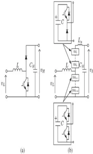
The ability to clamp the off-state voltage across a switch when a stack of switches is connected in series is crucial in forming MMC topologies. Using this idea, the modular multilevel inverter topology was generated by clamping the series-connected IGBTs in the conventional two-level inverter. With active clamping, each switch has a well-defined voltage and good sharing between sub modules. The active-clamping idea can also be applied to dc–dc converters. The upper IGBT in the half bridge is termed as clamping IGBT, whereas the lower IGBT is termed as clamped IGBT. The classic bidirectional two-level dc–dc converter is shown in Fig. 2(a). It consists of an inductor on the low-voltage side, two IGBTs with anti parallel diodes, and capacitors on both input and output sides. Replacing all the switches by series connected sub modules with active clamping, the bidirectional buck–
Fig. 2. Bidirectional dc–dc converters. (a) Conventional two-level dc–dc converter. (b) Novel modular multilevel
dc–dc converter.
III.HIGH STEP-UP RATIO MODULAR
MULTILEVEL DC–DC CONVERTER
This section describes the operation method for the proposed dc–dc converter. The analysis focuses on step-up dc–dc conversion. To simplify the analysis, the theoretical developments are based on the following assumptions.
1) The switches are ideal, and the sub modules are identical.
2) The converter is lossless.
3) In steady state, the capacitor dc voltages are balanced.
A.System Configuration
The configuration of the step-up conversion is provided to demonstrate the concept. The most commonly used boost converter topology with a single IGBT and a single diode is shown in Fig. 3(a). The IGBT in the lower position is used for charging the input inductor L. The diode in the upper position of the circuit is automatically commutated on when the inductor is discharging current to the high-voltage capacitor CH. Applying active clamping (see Fig. 1) to the two switches, the modular multilevel unidirectional step-up converter with two stacks of sub modules is obtained as shown in Fig. 3(b).
Fig. 3. Unidirectional step-up dc–dc converters. (a) Conventional boost converter. (b) Proposed modular
multilevel step-up dc–dc converter.
Fig. 4. Unidirectional step-down dc–dc converters. (a) Conventional buck converter. (b) Proposed modular
multilevel dc–dc converter.
B.Phase-Shift Control
The proposed converter has various operating modes resulting in different operating features and step-up ratios. Apart from the high step-up ratio operation mode, which is the focus of this paper, the converter can also be used for high step down ratio dc–dc conversion providing power for an auxiliary electronic circuit in medium-voltage systems. Moreover, with similar numbers of submodules in the upper stack and the lower stack, the converter can also be used for low-step-ratio high-voltage dc–dc conversion. Phase-shifted PWM is used to control the modular multilevel step-up dc–dc converter.
Phase-shifted PWM is arranged with a high duty cycle such that only one sub module capacitor at a time is out of the series connection, and thus, t he step-up ratio of the circuit becomes dependent on the number of upper cells N. The effective frequency of this excitation is much
cell. To demonstrate the principle of interleaved PWM, a step up converter with four sub modules in the diode position in the circuit of Fig. 3(b) is considered (N = 4). To ensure that either four or three sub modules are injecting voltage at any time, each must be operated with a duty cycle above 75%. For illustration, 90% is used. One module could be used in the lower position operating at four times the switching frequency of the upper modules (to give the same effective frequency). Instead, the system will be illustrated with two sub modules in the lower position operating at twice the frequency of the upper sub modules and with interleaved pulses.
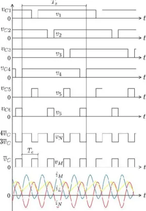
Fig. 5. Time-domain key waveforms of the proposed step-up converter.
Assuming the sub module capacitor voltages to be constant, the key waveforms of the sub module voltages are shown in Fig. 5. It can be seen in Fig. 5 that the upper (clamped diode) cells are synchronously switched with the lower (clamped IGBT) cells so that the total voltage of the upper cells vN and lower cells vM are complementary. This guarantees an almost constant dc voltage with a small ripple on the high voltage side. The equivalent operating frequency is four times the switching frequency of the upper cells (fe = 4fs ) and is twice the switching frequency of the lower cells.
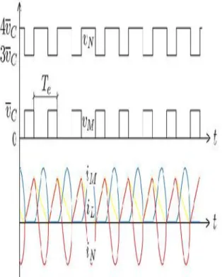
down operation has the same stack voltage waveforms as that of the step-up conversion. The voltage waveforms of the sub modules are not shown. The time-domain waveforms of the stacks are shown in Fig. 6. In the step-down operation, the current directions and waveforms are different from that in the step-down operation. The operation of step-down conversion will be analyzed in detail in the following section.
Fig. 6. Time-domain key waveforms of the proposed converter with step-down operation.
C.High Conversion Ratio
The proposed converter is aimed at high step-up ratio dc–dc conversion. The analysis of operation and conversion ratio will proceed by examining one equivalent cycle Te in Fig. 5. Fig. 7 shows the detailed circuit diagrams with current paths highlighted for the two modes of the circuit. Mode 1 starts when the IGBT in Cell 4 is switched on and ends when the IGBT in Cell 1 switches off [see Fig. 7(a)]. The IGBT in Cell 1 switches off when the lower IGBT in Cell 5 switches off, and this defines the beginning of Mode 2 [see Fig. 7(b)]. Mode 2 ends when the IGBT of Cell 1 is switched on again. Modes 1 and 2 are analogous to the on- and off-states of the simple boost converter but with the difference that current can flow in both paths in both modes. The current flowing through the input inductor, upper cells (clamped diodes), and lower cells (clamped IGBTs) are defined as iL, iN, and iM, respectively.
Fig. 7. Step-up operation modes in the first equivalent operating cycle. (a) Mode 1. (b) Mode 2
In Mode 1, the current iL of inductor L is directly charged by the low-side (input) voltage vL via the IGBTs in Cell 5 and Cell 6. The capacitors C1, C2, C3, and C4 are in series with the inductor L s and the high-side (output) capacitor CH, and together, they form a resonant tank. Because CH is large and the cell capacitors are smaller and placed in series, the resonance is dominated by the cell capacitors, and CH can be ignored. Therefore, the resonant frequency is
In the case of N = 4, fr = 1/π√LsC. When the
use the same capacitors, the resonant frequency in Mode 2 is the same as that in Mode 1.
In Fig. 7(b), it can be seen that the current iN cannot be negative in Mode 2 because one cell (Cell 1 in the figure) is acting as a diode. If the actual resonant frequency is slightly higher than fe, by the end of Mode 2, the current iN reaches zero, and the circuit operates in discontinuous conduction mode (DCM).
When Mode 1 begins, the current iL is directly charged by the low-side voltage source. Meanwhile, the current iN starts to resonate (starting from zero) with the frequency of fr. The current iM is iL minus iN. When the circuit enters Mode 2 from Mode 1, since vC5 is higher than vL, the inductor current iL reduces. As the circuit operates in DCM, before the end of the equivalent operating cycle, the current iN falls to zero, and the current iM is equal to iL until a new cycle begins. The simulation result later in this paper will illustrate this.
To obtain the voltage conversion ratio, the charging ratio d is defined as the time duration of Mode 1 relative to the period, i.e., Te of the equivalent operating cycle. In steady state, the increase and decrease of iL over a equivalent cycle Te should be the same; hence,
with j = 5 or j = 6. The capacitor voltages of the lower sub modules can be written as
The s um of average stack voltages vN and vM should be equal to the high-side voltage, i.e., vH, which yields
Under ideal conditions, the capacitor voltages are balanced and equal to vC. The voltage conversion ratio can be derived by substituting (3) into (4), i.e.,
It can be seen that without increasing d, the conversion ratio can be increased by using higher numbers of upper sub modules N. In the case of N = 4, the conversion ratio is vH/vL = 4/(1 − d). The current
stresses in the converter should be estimated because it is important in determining the power losses and device ratings. The low-side (input) inductor current iL comprises a dc component and a saw tooth-shaped ripple.
consumed on the high voltage side. Here, it is assumed that the load dc current is Io. Therefore,
The peak-to-peak ripple ΔIL can be obtained from the
charging time of inductor L, i.e.,
The current stress on the clamped-diode (upper) stack depends on iN. The dc component of iN goes on to feed the load, and its ac component circulates within the resonant tank. It will be assumed that the ac component of iN is approximately sinusoidal with a root mean square (RMS) value of IN1 at the resonant frequency. The power transferred out of the clampeddiode (upper) stack by the flow of the dc current is
On the other hand, the ac voltage of the upper stack is a square wave with a peak-to-peak value of vC. Therefore, the RMS value of this square wave is vC/2. The power transferred into the stack by the sinusoidal resonant current interacting with the square-wave component of the stack voltage is
with λ as the power factor for this voltage and current
combination. The value of λ can be obtained from numerical solutions. The maximum, i.e., λ = 1, is
achieved when the charging ratio is d = 0.5. If the converter is lossless, the dc power and ac power of the upper stack should be equal. Therefore
After iL and iN are estimated, the current stress on the lower stack can be determined by iM = iL− iN. A
rough estimation of |iM| < |iL| + |iN| can also be used. Although the converter is proposed for high step-up ratio dc–dc conversion, it also has the capability of step-down dc–dc conversion. Fig. 8 shows the detailed circuit diagrams with current paths highlighted for the two modes of the circuit. Mode 1 starts when the clamped IGBT in Cell 1 is switched on and ends when the clamped IGBT in Cell 1 is switched off [see Fig. 8(a)].
For operation analysis, the current directions are defined opposite to the current directions in the step-up operation. As the voltage on the inductor L in Mode 1 is higher than that in Mode 2, the current iL of inductor L is charged in Mode 1 and discharged in Mode 2. During Mode 1, the inductor Ls and the capacitors C2, C3, and C4 are charged, and therefore, the clamped diodes in the lower cells are reverse-biased. There is no current flowing through the lower stack. If the capacitor voltages are assumed to be constant, the currents iL and iN should linearly increase in Mode 1 and iL equals iN.
Fig. 8. Step-down operation modes in the first equivalent operating cycle. (a)Mode 1. (b)Mode 2
The slight increase in the cell capacitor voltages does not affect the wave shapes obviously. When the converter enters Mode 2 from Mode 1, all the cell capacitors in the upper stack are in series with the inductor L s. The inductor L starts to linearly discharge, and the clamped diode in Cell 6 is commutated. Meanwhile, the capacitors C1, C2, C3, and C4 in series with the inductor L s form a resonant tank to discharge the energy stored in the passive components from Mode 1. The resonant frequency fr in the step-down operation is the same as that in the step-up operation. Therefore, the current iM flowing through the lower stack can be written as
This analysis for step-down operation explains the current waveforms in Fig. 6. The inductor current has a sawtooth wave shape, and the lower stack current is zero during Mode 1. In Mode 1, the upper stack current is equal to the inductor current. In Mode 2, the upper stack current is discharging with a resonant wave shape, which, together with the inductor current, determines the lower stack current. To derive the step-down output voltage vL as a function of charging ratio d (defined in step-up operation) and high voltage vH, the inductor current iL is assumed to be the same after one equivalent charging cycle. Similar to the step-up operation, it can be approximated that Nv Cj = vH. The conversion ratio can be derived as
The step-down operation has the same step ratio function as that in the step-up operation. This means that the proposed modular multilevel dc–dc converter is similar to the conventional bidirectional dc–dc converter in terms of step ratio. By changing the current directions, the converter achieves bidirectional power conversion and the same step ratio without modifying t he switching arrangement.
1V.SIMULINK MODELLING AND RESULTS
4.1SIMULINK BLOCK
DIAGRAM
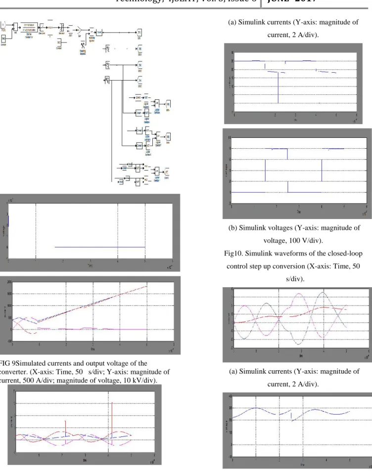
FIG 9Simulated currents and output voltage of the converter. (X-axis: Time, 50μs/div; Y-axis: magnitude of current, 500 A/div; magnitude of voltage, 10 kV/div).
(a) Simulink currents (Y-axis: magnitude of
current, 2 A/div).
(b) Simulink voltages (Y-axis: magnitude of
voltage, 100 V/div).
Fig10. Simulink waveforms of the closed-loop
control step up conversion (X-axis: Time, 50
μs/div).
(a) Simulink currents (Y-axis: magnitude of
(b) Simulink voltages (Y-axis: magnitude of voltage, 100
V/div).Fig.11. Simulink waveforms of the closed-loop
control stepdown conversion (X-axis: Time, 50 μs/div).
CONCLUSION
The new transformer less MMC dc–dc converter has been presented and analyzed. Two stacks of sub modules in series arrangement support the high voltage. This project is extended to next sub module for increasing operating range of the converter. The dc capacitors of the sub modules are used also for resonant operation. The proposed converter has a bidirectional conversion ability. The step-up operation and the step-down operation are demonstrated. This converter is capable of operating under open-loop control as a dc transformer with good linearity. Alternatively, closed-loop control can be applied for trimming of the output voltage
. The operating principle was verified through a simulation results . The proposed converter may exhibit relatively high losses because of the high ac current that resonates in the sub modules, but reasonably high efficiency was shown to be possible in high-voltage applications. Further efficiency improvement can be achieved with lower switching frequency, but cell capacitors with a higher volume will be required. The converter can achieve a large step-up conversion ratio without the use of transformers. The proposed converter has the features of modularity, scalability, and simplicity, and these may make it attractive in some special applications.
REFERENCES
[1] Xiaotian Zhang, Member, IEEE, and Timothy C. Green, Senior Member, IEEE” the modular multilevel converter for high step-up ratio dc–dc conversion”2015
paper
[2] S. Kouroetal., “Recent advances and industrial applications of multilevel converters,” IEEE Trans. Ind.
Electron., vol. 57, no. 8, pp. 2553–2580, Aug. 2010.
[3] J. I. Leon et al., “Multidimensional modulation
technique for cascaded multilevel converters,” IEEE
Trans. Ind. Electron., vol. 58, no. 2, pp. 412– 420, Feb. 2011.
[4] E. Solas et al., “Modular multilevel converter with
different submodule concepts—Part II: Experimental validation and comparison for HVDC application,” IEEE
Trans. Ind. Electron., vol. 60, no. 10, pp. 4536–4545, Oct. 2013.
[5] J. Ferreira, “The multilevel modular dc converter,”
IEEE Trans. Power Electron., vol. 28, no. 10, pp. 4460–
4465, Oct. 2013.
[6] M. Perez, S. Bernet, J. Rodriguez, S. Kouro, and R.
Lizana, “Circuit topologies, modelling, control schemes and applications of modular multilevel converters,” IEEE
Trans. Power Electron., vol. 30, no. 1, pp. 4–17, Jan. 2015.
[7] T. A. Meynard and H. Foch, “Multi-level conversion: High voltage choppers and voltage-source inverters,” in
Proc. IEEE Power Electron. Spec. Conf., 1992, pp. 397–
403.
[8] F. Z. Peng, “A generalized multilevel inverter topology with self voltage balancing,” IEEE Trans. Ind.
Appl., vol. 37, no. 2, pp. 611–618, Mar./Apr. 2001.
[9] S. Busquets-Monge, S. Alepuz, and J. Bordonau, “A
bidirectional multilevel boost–buck dc–dc converter,”
IEEE Trans. Power Electron., vol. 26, no. 8, pp. 2172–
2183, Aug. 2011.
[10] T. Todorcevic, P. Bauer, J. A. Ferreira, and R. van
Kessel, “Bidirectional modular multilevel dc–dc converter control and efficiency improvements through
separate module control method,” in Proc. IEEE Energy
Convers. Congr. Expo., 2013, pp. 2038–2043.
[11] K. D. T. Ngo and R. Webster,“Steady-state analysis and design of a switched-capacitor dc–dc converter,”
IEEE Trans. Aerop. Electron. Syst., vol. 30, no. 1, pp. 92–101, Jan. 1994.
[12] F. Khan and L. Tolbert, “A multilevel modular
capacitor-clamped DC–DC converter,” IEEE Trans. Ind.