http://www.sciencepublishinggroup.com/j/ajpa doi: 10.11648/j.ajpa.20170505.11
ISSN: 2330-4286 (Print); ISSN: 2330-4308 (Online)
Construction of Sheet Resistance Measurement Setup for
Tin Dioxide Film Using Four Probe Method
Rikesh Bhattarai
1, Shankar Prasad Shrestha
2, *1Department of Physics, Tri-Chandra Multiple Campus, Kathmandu, Nepal 2
Department of Physics, Patan Multiple Campus, Patandhoka, Nepal
Email address:
[email protected] (R. Bhattarai), [email protected] (S. P. Shrestha) *
Corresponding author
To cite this article:
Rikesh Bhattarai, Shankar Prasad Shrestha. Construction of Sheet Resistance Measurement Setup for Tin Dioxide Film Using Four Probe Method. American Journal of Physics and Applications. Vol. 5, No. 5, 2017, pp. 60-65. doi: 10.11648/j.ajpa.20170505.11
Received: January 16, 2017; Accepted: January 25, 2017; Published: August 3, 2017
Abstract: The main purpose of the paper is to construct the four probes to calculate the sheet resistance the thin film. For the
thin film this paper presents the experimental preparation of Tin dioxide thin films. A dual voltage power supply and constant current source is developed to study deeply for the constant current output. Electrical properties are measured using constant current source, sheet resistance, four probe), digital multimeter and micro ammeter. The effect of thickness of sheet resistance thin film is carried out by four probe method.Keywords: Tin Dioxide, Four Probe, Spin Coating Method, Sheet Resistance
1. Introduction
Nano-crystals of semiconductor metal oxides have attracted a great interest due to their intriguing properties, which are different from those of their corresponding bulk state. Tin Oxide (SnO2) is one of the important metal oxides due to its many useful properties such as its wide band gap 3.6-3.8 eV, n-type conductivity and high transparency in the visible range [1]. Most of the oxides including Tin dioxide are used as gas sensors [2]. Tin oxide is also a viable semiconductor candidate to replace the wind gap zinc oxide layer window to improve the long term the device reliability. Amorphous tin oxide may be used as a glass over layer for covering for entire device and protecting it against water permeation. The research and development on thin film technology have been increasing rapidly over the past two decades due to their vast applications in almost all fields of science and technology. It is utilized in many commercial applications such as anti- reflection coatings, liquid crystal displays, and piezoelectric, electro- and photo-luminescent devices, chemical and biological sensors. Tin dioxide thin films and micro and nanostructures are very promising candidates for novel applications in emerging thin-film transistors, solar cells, sensors and optoelectronic devices.
The topic of tin dioxide thin films has been studied intensively in the recent years due to their promising electrical and optical properties, concurrent with the rise of emerging thin film technologies particularly in large area electronics (LAE), displays, sensors, piezoelectric, optoelectronic, and photovoltaic (PV) devices [3].
There are several methods for preparation of tin oxide thin films some of them are Spray pyrolysis, Deep coating, Sol-gel method, Spin coating method, Adsorption and reaction method, Chemical vapor deposition etc. Most of these deposition techniques are broadly divided into two categories: physical vapor deposition processes and chemical processes. Physical vapor deposition processes include Pulsed laser deposition, sputtering (magnetic and Radio Frequency, RF) while chemical processes are chemical deposition, sol gel and metal organic chemical vapor deposition and liquid phase etc [4].
2. Film Deposition and Characterization
2.1. Experimental
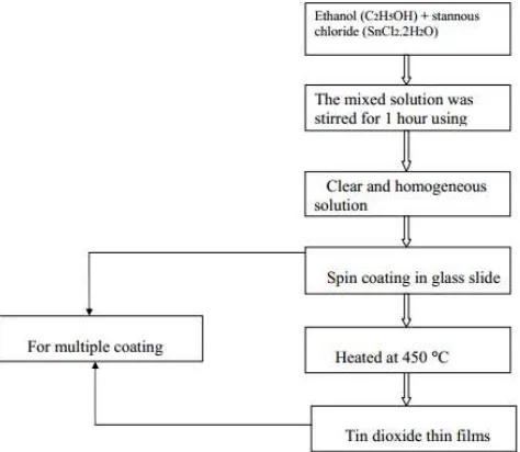
chloride (SnCl2.2H2O) mixed in 25 ml ethanol (C2H5OH) at room temperature. The mixed solution was stirred for 1 hour using magnetic stirrer to yield a clear, homogeneous and transparent solution and precursor solution was obtained by filtrating through filter paper. Then the tin oxide film was prepared by using a homemade spin-coating apparatus, which consists of a precursor container, a step motor and a heater. The layer-by layer deposition cycle was done by alternating between dip-coating a thin layer and drying in air after each new layer. The resultant Tin dioxide solution so prepared was stirred in magnetic stirrer for two hours to get a clear homogeneous solution maintaining the constant temperature of 80-90°C, the solution was then stored in a air tight beaker as stock solution.
The substrate are generally required cleaning before the film deposition because of the dust and impurities particles on the surface of the substrate. This can adversely affect the growth of the films and also lead to the inclusion formation of many impurities. Hence it is important to clean substrate properly before placing into the film deposition technique. The procedure of cleaning is as follows. The substrates were put into a bath of water with detergent to remove dirt and oil from the substrate. Then the substrates were washed once more by using de-ionized water and acetone. Acetone or ethanol tends to live some spots on the surface of the substrate. After the final wash the substrate were dried in heater.
Figure 1. Flow chart of the preparation of Tin dioxide thin film.
The prepared SnO2 precursor is dripped on to the substrate (glass slides) through the dropper placed on spin coater. Few drops (5-8) drops of the solution were added drop wise on the glass substrate which was kept on the home made spinner after cleaning. The drops were sprayed on the glass substrate to get uniform deposition. The home made spin coater was rotated at the speed of around 300-400 rpm for about 30 sec to get more homogeneous and uniform coating. The substrates were taken from spin coater using forceps carefully for pre heating over the marble placed above heater
at temperature about 200°C for about 5 minutes, and then the slide was then taken out on the preheating plate and cooled for sometimes to prevent from cracking due to the abrupt change in temperature. The slides were again spin coated using the same procedure as it was done earlier. The prepared samples were heated for zero hour, 1 hour, 2 hours and 3 hours separately electrical characterization.
The process was repeated for two more coatings making it 4-coated thin film of tin dioxide followed by annealing procedure.
2.2. Electrical Characterization
Basically, the electronic transport properties of semiconductors depend upon the characteristics of mobile electrons. The electrical properties are studied by measuring sheet resistance and resistivity. The measurement technique for each property is described separately.
2.2.1. Regulated Power Supply
A power supply is an electronic device that supplies electric energy to an electrical load. The primary function of a power supply is to convert one form of electrical energy to another and, as a result, power supplies are sometimes referred to as electric power converters. Some DC power supplies use AC mains electricity as an energy source. Such power supplies will sometimes employ a transformer to convert the input voltage to a higher or lower AC voltage. A rectifier is used to convert the transformer output voltage to a varying DC voltage, which in turn is passed through an electronic filter to convert it to an unregulated DC voltage. The filter removes most, but not all of the AC voltage variations; the remaining AC voltage is known as ripple. The electric load's tolerance of ripple dictates the minimum amount of filtering that must be provided by a power supply. In some applications, high ripple is tolerated and therefore no filtering is required. For example, in some battery charging applications it is possible to implement a mains-powered DC power supply with nothing more than a transformer and a single rectifier diode, with a resistor in series with the output to limit charging current.
Figure 2. Dual voltage power supply (12 Volt) [6].
a rectifier it converts AC supply into DC. Its function is to supply a stable voltage (or less often current), to a circuit or device that must be operated within certain power supply limits [5].
The output from the regulated power supply may be alternating or unidirectional, but is nearly always DC (Direct Current).
2.2.2. Constant Current Source
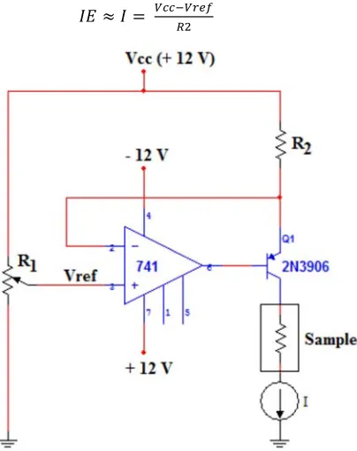
A current source is an electronic circuit that delivers or absorbs an electric current which is independent of the resistance across it. A current source is the dual of a voltage source. The term, constant-current sink, is sometimes used for sources fed from a negative voltage supply. An independent current source (or sink) delivers a constant current [7]. A constant current source is a power generator whose internal resistance is very high compared with the load resistance it is giving power to. Because its internal resistance is so high, it can supply a constant current to a load whose resistance value varies, even over a wide range. Thus, a constant current source follows the rules of current division. Being that it has very high internal resistance and the load resistance is much lower, current takes the path of least resistance, flowing out of the (high internal resistance) current source and into the load resistance, since it is of much lower resistance. The following circuit figure 3 is voltage controlled current source [8], with slight modifications. Since the collector and emitter currents of the transistor are almost equal, the current through R2 is approximately equal to the load current (I). Because of the virtual short between the op-amp inputs, the inverting input voltage approximately equals Vref. Therefore, the voltage across R2 equals Vcc– Vref and the current through R2 is given by
(1)
Figure 3. Voltage controlled current source.
In this circuit, load current I decreases when the input reference voltage increases. And the maximum load resistance can be calculated as
(2)
Figure 4. Important measurements on the experimental setup.
Theoretical calculation for load current and maximum load resistance:
The load current
2
.
! " =40 Microampere
The maximum load resistance at this 40 µA current
(3)
160 ! 10& 12
5.56 1
RL= 138136.65 Ohm
The load current 0.040 mA remains constant throughout the measurement.
2.2.3. Four Probe, Sheet Resistance and Resistivity
Four-terminal sensing (4T sensing), wire sensing, or 4-point probes method is an electrical impedance measuring technique that uses separate pairs of current-carrying and voltage sensing electrodes to make more accurate measurements than the simpler and more usual two-terminal (2T) sensing. Four point probes are also used to measure sheet resistance of thin films. Separation of current and voltage electrodes eliminates the lead and contact resistance from the measurement. This is man advantage for precise measurement of low resistance values [9].
that are nominally uniform in thickness. It is commonly used to characterize materials made by semiconductor doping, metal deposition, resistive paste printing, and glass coating. Examples of these processes are: doped semiconductor regions (e.g., silicon or polysillicon), and the resistors that are screen printed onto the substrates of thick-film hybrid microcircuits. The utility of sheet resistance as opposed to resistance or resistivity is that it is directly measured using a four-terminal sensing measurement or indirectly by using a non-contact eddy current based testing device. Sheet resistance is invariable under scaling of the film contact and therefore can be used to compare the electrical properties of devices that are significantly different in size [10].
Semiconductor has electrical conductivity intermediate in magnitude between that of a conductor and insulator. Semiconductor differs from metals in their characteristic property of decreasing electrical resistivity with increasing temperature. According to band theory, the energy levels of semiconductors can be grouped into two bands, valence band and the conduction band. In the presence of an external electric field it is electrons in the valence band that can move freely, thereby responsible for the electrical conductivity of semiconductors. In case of intrinsic semiconductors, the Fermi level lies in between the conduction band minimum and valence band is maximum. Since conduction band lies above the Fermi level at 0K, when no thermal excitations are available, the conduction band remains unoccupied. So conduction is not possible at 0K, and resistance is infinite. As temperature increases, the occupancy of conduction band goes up, thereby resulting in decrease of electrical resistivity of semiconductor. Semi- conductors are generally classified by their electrical resistivity at room temperature, with value range of 102 and 109 ohm-cm, and strongly dependent on temperature [11]. At absolute zero, a perfect crystal of most semiconductors will be an insulator. The properties of as deposited thin films semiconductors can be explained on these bases. The sheet resistance for any rectangular shaped thin films, is given by
()
*+ (4) Where, l, b and d are length, breadth and thickness of the rectangular shaped thin films which is shown in figure 5. The sheet resistance is very useful quantity, which is widely used to resistivity of films particularly those of the same material deposited under similar conditions. For square base, l=b the sheet resistance is given by
(
+ , (5) This shows that the resistance RS of one square of thin film is independent of size of the square and depends only the resistivity and thickness of the film. The quantity RS is called the sheet resistance of the film and is expressed in ohms per square. If the thickness is known then the resistivity can be readily obtained by using the relation RS
- ,. . (6)
Figure 5. Definition of Sheet resistance.
The most direct method of measuring RS is to prepare a rectangular sample of thin as its resistance, and divide by number of squares of films materials that lie between the end contacts. Where contact resistance between the film and the end terminals may be a problem, a four probe method is necessary. The four probe method is discussed in subsequent section. The numbers of squares now in this case is counted between the two voltage terminals and
/ (7) Resistivity: Resistivity of thin film was measured using four probe method.
-/
0 1
213 1 24
1 5216247
1 52462"7
(8)
When S1 = S2 = S3 = S, then above equation becomes
-/289 (9) If the material on which the probes are placed is an infinitely thin slice resting on aninsulating support, the above equation becomes
-/ 0+
:; (10) The sheet resistance is given by RS
(
+ , 4.532/……… (11)
3. Result, Graph and Discussion
In the present work we have studied the electrical properties of the deposited SnO2 thin films. Films were prepared by spin-coating technique. We have studied the constant current source, electrical characterization: sheet resistivity using spin coating technique. The data reading were analyzed by making graphs of constant current source and resistivity with the help of origin software. The results of our experimental measurements are discussed below.
For the constant current source, the current is varying from the potentiometer which changes the current in the circuit. We have measured current through the sample for different low resistance.
Figure 7. Graph for observed current at 40 microampere.
We have measured the current through the sample for different load resistance. Figure 7 shows that the observed current for different load resistance of initial current set up at 40 microampere.
Figure 8. Graph for observed current at 10 microampere.
We have measured the current through the sample for different load resistance. Figure 8 shows that the observed current for different load resistance of initial current set up at 10 microampere.
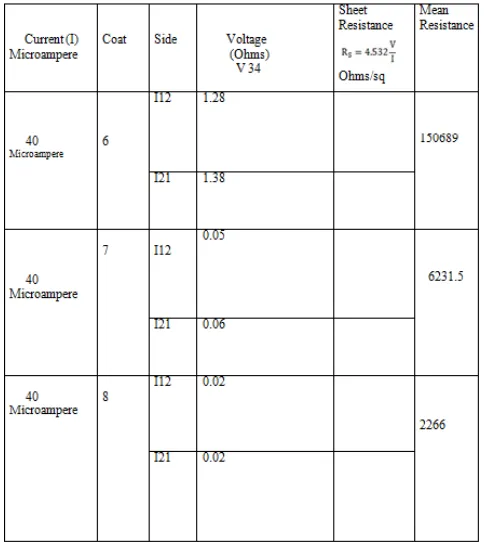
In the below table, data obtained from the experiment by using different coated thin films of tin oxide. For the constant current, we use constant current source and four probe linear arrangements, and setup experimental arrangement and obtain different values of voltage for different coating thin film of tin oxide. The value of sheet resistance (RS) is obtained by applying equation (11).
Figure 9. Shows the graph between sheet resistances for different coated thin films of tin dioxide following nature.
Figure 10. Observed graph of sheet resistivity vs. number of coat.
film sheet resistance is high than the 7th and 8th coating. Thus we can conclude that as the number of coating increases, sheet resistance decreases.
4. Conclusion
Tin oxide (SnO2) films of varying thickness were successfully synthesized on glass plate by spin coating method by using stannous chloride (SnCl2:2H2O) as a precursor in ethanol (C2H5OH). Electrical characteristics are studied developing the four probes without heating effect. The electrical characteristics were obtained by using constant current source and four probe arrangements. The sheet resistance, voltage increases with decrease in the number of coating the thin films. We found the sheet resistance of 6th coat is greater than 7th and 8th coat.
Acknowledgements
I would like to express the deepest appreciation to Prof. Dr. Shankar Prasad Shrestha and Mr. Hari Shankar Mallik for the convincingly conveyed a spirit of adventure and guidance in regard to research. We acknowledge the support of Tribhuvan University for providing a laboratory.
References
[1] Patil Ganesh E., Kajale DD., Chavan DN., Pawar NK., Ahire PT., Shinde SD, Gaikwad VB. and Jain GH. (February 2011). Synthesis, characterization and gas sensing performance of SnO2 thin films prepared by spray pyrolysis, Bull. Mater. Sci., Vol. 34, No. 1, pp. 1–9.
[2] Optical properties of spin coated Cu doped ZnO nanocomposite films, P. Samarasekara and Udumbara. [3] Ng ZiNeng, Fabrication and characterization of ZnO thin
films using Sol-Gel spin coating.
[4] G. G. Valle, P. Hammer, S. H. Pulcinelli and C. V. Santilli, “Transparent and Conductive ZnO: Al Thin Films Prepared by Sol-Gel Dip-Coating,” Journal of European Ceramic Society, Vol. 24, No. 6, (2004), pp. 1009-1013. doi: 10.1016/S0955-2219(03)00597-1.
[5] https://en.wikipedia.org/wiki/Regulated_power_supply [6]
http://www.electronics-lab.com/project/dual-voltage-power-supply/
[7] https://en.wikipedia.org/wiki/Current_source [8] Malvino, Electronic Principles, 6thed
[9] https://en.wikipedia.org/wiki/Four terminal_sensing [10] https://en.wikipedia.org/wiki/Sheet_resistan elm