INTRODUCTION
The study on the depletion layer of the p-n jup-nctiop-n has aroused the ip-nterest of 1-5 map-ny investigators . The main purpose is to increase the efficiency of the p-n junction as a solar energy converter. The depletion layer is an effective part of the indicated device. Thus the trend to determine the main character istics of such a layer is predominant.
The present study is based on a model according to which the charges within the depletion layer are distributed on its lateral sides as surface charge distribution.
This model is in contrast with that model suggesting volume charge distribution in the depletion layer, for which Poisson’s equation is required to find the potential. The application of both models will affect the estimated values of its
On the depletion layer
M.K. EL-ADAWI* and N.S. AL-SHAMERI
Physics Department, Faculty of Science for Girls-King Faisal University P.O Box 838, Dammam - 311 13 (Saudi Arabia).
(Received: February 20, 2009; Accepted: April 28, 2009)
ABSTRACT
The main characteristics of the depletion layer, are obtained on the basis of a suggested model, according to which, the charge is distributed, not as a space charge but as surface charge on the lateral sides of the depletion layer.
Comparative discussions of the results obtained according to both models are given. The dependences on the ratio ‘’
a d N N
‘’ and the applied voltage ‘’ Va‘’ are clarified. Both forward and
backward biases are also considered. Graphical representations for the obtained relations, considering an illustrative example on a silicon cell are also given.
Key words: Depletion layer, charge, silicon cell.
characteristics. This in turns will affect the expected values of the efficiency for such a device.
Derivation of the basic equations
Let us assume that the surface densities of the charge on the lateral sides of the depletion layer are given as:
...(1)
and
...(2)
Where
,
d a
N
N
,3
m
−Donor and acceptor impurity
densities, respectively.
,
n p
, 3
m
−Densities of free electrons and holes,
respectively.
q
,
C
According to Gauss theory, the intensity of the electric field (E), in the neighborhood of a charged plane surface is given according to the relation
...(3)
Where
ε
, is the permittivity of the medium ε0,F/m is the permittivity of free space,r
ε is the relative permittivity Moreover, one has to consider the relation
...(4)
The boundary conditions imposed on the potentials fig (1) can be summarized as follows:
Where is the built in potential.
The system of equations (3 ) , (4 ) and (5) makes it possible to obtain the following results:
...(6)
...(7)
Equation (6) and (7) are subjected to the continuity condition at
x
=
x
0 , namely:...(8)
This gives, the following results:
...(9)
and
...(10)
Fig. 2: The thickness of the depletion layer as a function as a function of the dopping ratio Φ
Vbi
p
n
x1 x0 x2 X
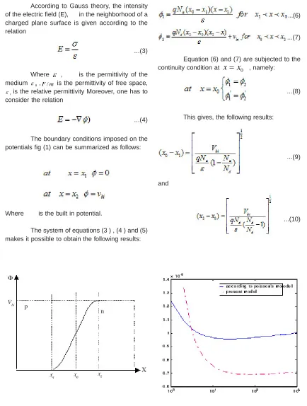
Fig. 3: The thickness of the depletion layer as a function of the applied
voltage-comparative study
(Backward bias) (Forward bias)
Fig. 4: The thickness of the depletion layer as a function of the applied
voltage -comparative study
Fig. 5: The capacity as a function of the dopping ratio
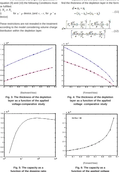
Fig. 6: The capacity as a function of the applied voltage
(Forward bias)
It is revealed, that to get real quantities, in equation (9) and (10) the following Conditions must be fulfilled.
i)
N
d≠
N
aii)
a
d N
N f
for n+ p device, (and NafNd for
p
n
+
device)
These restrictions are not revealed in the treatment according to the model considering volume charge distribution within the depletion layer.
Equations (9) and (10) make if possible to find the thickness of the depletion layer in the form:
...(11)
Fig. 7: The capacity of the depletion layer as function of the applied voltage
(Backward bias)
Fig. 8: The capacity as a function of the applied voltage-comparative study
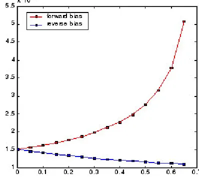
Fig. 9: The thickness as a function of the applied voltage-comparative study
Where, the built in potential
v
bi is given in literatures asWhere
i
n
, −3m
Intrinsic density T, 0K
Absolute temperaturek
,J
0K
/
Boltzmann constantThe capacity of the depletion layer as a parallel plate condenser can be obtained through the relation:
...(13)
Where, s, 2
m
is the surface lateral area of one side.Computations and discussion
Let us consider a n+ pjunction made of silicon having the following specifications
0
300
T
=
K
19
1.6 10
q= × − C, Na 1021m3,Nd 1023m3,n2i 1032m6
− − −
= = =
This result shows that the metallurgical surface is nearer to the side with higher doping concentration.
Moreover, the obtained expressions and computations reveal that for higher values of the ratio
a d
N N
, one obtains smaller values for the thickness of the depletion layer than those obtained according to the other model and vice versa. At a critical ratio one gets equal values for the thickness according to both models. The thickness ‘’d’’ as a function of shows asymptotic behaviour. The asymptotic value of the thickness in case of our model is smaller than that according the other model, as shown in fig (2).
The thickness as a function of the applied voltage Va is also studied for the forward and
backward biases, and compared with corresponding values according to Poisson’s model .The obtained results are illustrated graphically in figures (3) , (4) and (9).
The thickness of the depletion layer as a function of the applied voltage –comparative study
Computations for capacity reveal that it does increase with
a d N N
ratio and it shows asymptotic behaviour, as shown in fig (5).
The dependence of the capacity on the applied voltage reveals that for forward bias, it increases with Va while, it decreases with for
backward bias, as sown in figures (6) , (7) and (8).
CONCLUSIONS
As a result of this study, the following conclusions can be given
´ The introduced model that assumes surface charge on the lateral sides of the depletion layer gives smaller values for the thickness of the depletion layer and the capacity of the equivalent condenser than that obtained for the model that assumes volume charge distribution in the space of the depletion layer, for the same parameters.
´ Asymptotic behavior for the thickness as a function of the ratio
a d N N
is clarified. ´ The condition ≠1
a d N N
is established.
´ Moreover, two other conditions are obtained namely:
i) f1 a d
N N
for n+ p device.
ii) p1 a d
N N
for p+n device, such conditions are not established when the model of volume charge distribution in the depletion layer is considered.
For forward bias, the capacity of the depletion layer increases with the increase of the applied voltage and vice versa for the case of backward bias. This article is of importance in the efficiency evaluation of the solar energy converter. Further, studies are required to reveal the effect of the obtained results on the efficiency of the solar energy converter.
1. Lucia, M.L., Herandez-Rojas, J.L., Leon, C., and Martil, I.. Capacitance measurements of p-n junction: Depletion layer and diffusion capacitance contributions. European Journal of Physics.14: 86-89 (1993).
2. Charabarty, K., Nsingh, S.. Depletion layer resistance and its effect on I-V characteristics of fully-and partially-illuminated silicon solar cells. Solid State Electronics. 39(4): 577-581(1996).
REFERENCES
3. Carrido, C.L., Stolik, D., Rodriguez, J., and Morales, A.. Influence of carrier recombination in the space charge region on minority carrier life time in the base region of solar cells. Solar Energy Materials & Solar cells. 57: 239-247(1999).
Instruments & Methods in Physics Research. A495: 232-234 (2002).
5. Kosyachenko, L.A., Ostapov, S.E., Markov, A.V., and Rarenko, I.M. Electronic transport properties of HgMnTe n+p junction. Infrared Physics & Technology. 44: 1-10 (2003).. 6. Kano, A. Semi conductor devices,
Prentice-Hall, (1998). USA.
7. Pierret, R.F Semi conductor devices fundamentals, Addison-Wesleypublishing Company, .(1996). USA.
8. Green, M.A. Solar cells, Prentice-Hall, Englewood Cliffs. (1982).