Puspa Raj Adhikari et al./ BIBECHANA 16 (2019) 7-14 : RCOST p.7 (Online Publication: Dec., 2018)
BIBECHANA
A Multidisciplinary Journal of Science, Technology and Mathematics
ISSN 2091-0762 (Print), 2382-5340 (0nline)
Journal homepage: http://nepjol.info/index.php/BIBECHANA
Publisher: Research Council of Science and Technology, Biratnagar, Nepal
Abstract
Nanowires are the one-dimensional nanostructures with the diameter order of one to few hundred nanometres. These structures show unique properties other than their bulk structures. In this article, a qualitative first principle discussion of TiC nanowire is reported, indicating the impact of DFT based GGA relativistic corrections on its electronic properties. Here, we analyse the Titanium Carbide (TiC) nanowire of hexagonal structure periodic in Z-direction with the density functional theory (DFT). The GGA with RBBE Correlation analysis of this material shows the metallic characteristics in its bulk but the electronic density of state shows that the hybridization states are different from their bulk when the material is analysed in nanostructure form. Three structures of hexagonal TiC nanowire directed in (1,1,1) plane were analysed to explore diameter (4-18) Å dependent comparative study of electronic, stabilizing and optical property which shows unique different result counterparts to its bulk. Hexagonal TiC nanowire were found to be semiconducting with narrow band gap (0.21-0.34) eV in small diameter while metallic in higher diameter. They are comparable stables as their bulk for higher structure. Similarly, for the same investigation, the structures are cross checked by surface atom passivation to verify the reliability of the result that we found.
Keywords: Nanowire, DFT; DOS; Band structure; Binding energy; Density of state; Hydrogen passivation.
1.Introduction
Depending upon the structures, Nanowires forms different periodic linear shape, so that they can be taken as 1-dimensional Nano-structure. They show many interesting properties that makes them a https://creativecommons.org/licenses/by-nc/4.0/
This work is licensed under the Creative Commons CC BY-NC License. DOI:https://doi.org/10.3126/bibechana.v16i0.20865
Article history: Received 3 February, 2018; Accepted 23August, 2018 *E-mail:[email protected]
5Hydra Research and Policy Center, Kathmandu, Nepal
4Department of Physics, Tribhuwan University, Kirtipur, Nepal.
3ABV-Indian Institute ofInformation Technology and Management, Gwalior, M.P–474010, India. 2Central Department of Physics Tribhuvan University, Kirtipur, Nepal
1Patan Multiple Campus, Tribhuwan University, Lalitpur, Nepal
PuspaRaj Adhikari1,3,Om PrakashUpadhyay1, Gopi Chandra Kaphle1,2,4,*, Anurag Srivastava3
initio study
potential candidate in wide variety of application [1] in nanotechnology, electro- optical, mechanical and many more fields of academic to industry[2-3]. The research of nanotechnology is not much older than other but the acceleration on this field is 10 times over for this recent Decades. The eco-friendly behaviour and clean energy application of the nanomaterial are the great attraction to researchers that makes the efficient and durability to this field. To develop a fundamental understanding and application to excellent properties shown by the nanostructures are the main goals of nanostructure investigation[4]. The first discovery of the 1-D nanotube by Iijima 1991 blow stream to research on nanostructure [5] and spread much excitement to the researchers due to demonstration of extraordinary properties. The reduction on the dimensional and size of the material enable the quantum confinement due to which material shows unusual behaviour [5,6] to its bulk Counter parts. Such effects in Nanostructure’s are called quantum mechanical effect. The variety of nanowires (semiconducting nanowire (Si) [7], magnetic nanowire (Ni, Pt) [6,8], dielectric nanowire (SiO2, TiO2)[9] and other inorganic molecular nanowire (MO6S9-x7x) [10] are successfully investigated and analysed till the date. These show the drastic change on Nano sized electronic application such as nanoscale quantum device, biomolecular nonsense and optoelectronic device over the old fashion material device.
TiC bulk is a face cantered cubic (fcc) crystal with rocksalt type structure. The lattice parameter (a) of this crystal is 4.3186 Angstrom with space group of 225 [11]. The Pearson symmetry notation is cFn but often represented by Fm3m in Hermann-Mauguin notation. Basically it is found in back powder form [12] but referred as the strong reinforcement material [13]. This material has unique property that it is corrosion resistance material so that its application is high for thermal shock wear, cutting tool and hard military application [13-14]. It is metallic in nature in its bulk with no spin polarization and referred as paramagnetic material. Due to high hardness, Titanium carbide is taken as the excellent mechanical material. On addition, due to high melting and boiling point of this material, its demand for the wear equipment is high. Recently Andrey et. Al. [16] theoretical dftb study shows that one-dimensional TiC nanotubes are semiconducting and electronic properties are diameter dependent. Similarly, Kaifu et. Al. [17] synthesis the TiC nanowire of 20-30 Å with good emission stability. In these Nano-sized structure, the quantum mechanical effect come to play to show different unexpected properties. These properties demands more study and investigation of nanoscale structure to explore more important properties in the recent technological application. Here we also aspect that the one dimensional TiC nanowire must show some unique property rather than its bulk.
2.Structure and computational details
Puspa Raj Adhikari et al./ BIBECHANA 16 (2019) 7-14 : RCOST p.9 (Online Publication: Dec., 2018)
energy structure to calculate the Nobel property at ground state. The force tolerance and stress tolerance are kept 0.05 eV/Å and 0.1 Gpa during the self-consistent force optimization. The energy range 0 eV to 5 eV is taken to observe the optical spectrum where 10 band below the fermi level and 20 bands above the fermi level are taken into consideration. For the next part of comparative study, the dangling bonds of surface atoms are passivated by Hydrogen to analyze the significant effect on electronic and optical property.
(a) (b) (c)
Fig. 1: Systematic Structures of (a) bulk TiC crystal at 2*2*2 repetition (b) Hexagonal TiC nanowire (111) plane and (c) H-Passivated hexagonal TiC nanowire.
3.Results and discussions
In order to investigate the stability of formation of TiC Nanowire, first we calculate the total energy of the whole structure and each free atom. With these data, the stability of the nanowire in increasing diameter has been calculated. To observe the electric behaviour of each nanowire the electron base structure and density of state has been computed taking same functional.
3.1. Structural Stability
In order to study the structural stability of the nanowire, the total binding energy for each structure is calculated. The structures with low total energy with high binding energy are said to be stable in the structural form and possess low energy system. The total energy of each freely optimised structure is calculated and the free energy of each individual atom Ti and C are calculated separately. The free energy of individual Ti atom is found to be ET(Titanium)= -174.083 eV and individual C atom is found to be ET(Carbon)=-148.182eV. Then by using the binding energy formula,
𝐸𝐵 =
[𝑝 ∗ 𝐸𝑇(𝑇𝑖𝑡𝑎𝑛𝑖𝑢𝑚) + 𝑞 ∗ 𝐸𝑇(𝐶𝑎𝑟𝑏𝑜𝑛)– 𝐸𝑇(𝑇𝑖𝐶)]
𝑝 + 𝑞
where,
𝐸𝐵 =
[𝑝 ∗ 𝐸𝑇(𝑇𝑖𝑡𝑎𝑛𝑖𝑢𝑚) + 𝑞 ∗ 𝐸𝑇(𝐶𝑎𝑟𝑏𝑜𝑛) + 𝑟 ∗ 𝐸𝑇(𝐻𝑦𝑑𝑟𝑜𝑔𝑒𝑛)– 𝐸𝑇(𝑇𝑖𝐶)]
𝑝 + 𝑞 + 𝑟
The stability calculated for each structure determines its probability to obtain during synthesis as the major product on applying some appropriate external parameter. These principles suggest that the higher diameter TiC nanowire can be synthesized more extent due to their more stability than the lower diameter nanowire. The graphical representation of stability of nanowire with varying its diameter is as shown in figure.
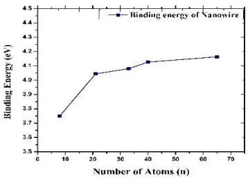
Fig. 2: Systematic graph plot of Binding Energy variation with number of atoms of TiC Nanowire.
From graph of stability vs. diameter of structure shows that when the number of atoms on structure increases, the binding energy of each atoms also observed to be increases. This suggests that the structure containing more atom, binding energy between atoms also increases and stability tends to approximately to its bulk structure. Naturally, the intrinsic bulk structure are most stable form in nature. Finally, the higher structures leads to the most stable NWs among the considered surface configurations with binding energies that are even close to the bulk limit.
But, unfortunately the passivated structure become distorted during their optimization calculation. This theoretical investigation upon H-passivated TiC nanowire suggest that passivation doesn’t account the dangling bonds of nanowire [18]. The molecular dynamics picture over the optimization shows that the passivated hydrogen atoms try to takes the position at the interior vacant part of nanowire and then bonded between interior atoms and edge of exterior dangling bonds. The observed total energy of the structure is decreases in some extent nut the shape and size of the structure are much more distorted in higher diameter nanotube.
3.2. Electronic properties
Puspa Raj Adhikari et al./ BIBECHANA 16 (2019) 7-14 : RCOST p. 11 (Online Publication: Dec., 2018)
3.2.1 Electronic Band gap
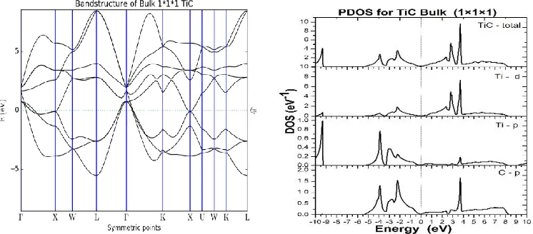
Fig. 3: Band structure Plot and Partial Density of States plot of Titanium Carbide Bulk.
The band gap calculation of TiC nanowire found to be interesting. The smallest structure of nanowire under my calculation shows that its electronic behaviour lies on semiconducting while its bulk counterpart is pure metallic in nature. On increasing Diameter of nanowire, the band gap of structure decreases gradually decreases and all structures of TiC nanowire become metallic when their diameter exceeds the size of 8.5 Å which suggest that the smaller diameter nanowire are semiconductor having direct band gap while higher diameter nanowire are metallic in nature along (1,1,1) crystallographic plane. The plot of observed band gap of structure vs. diameter are represented as below.
The observed semiconducting nanowire of Titanium carbide have very narrow bandgap about (0.2-0.35)ev which are also direct bandgap in nature. The narrow band gap structure with direct nature semiconducting material are supposed to be very important for the choice of many applications in the infrared region. Because in wide band gap semiconductors (band gap greater than Si) are not desirable for bipolar devices due to higher difference in mobility of electrons and hole for power application. The narrow band gap semiconducting materials are building block for novel tunnel devices and infrared super lattices [19]. Simple K-P theory suggest that the small gap materials basically means small effective mass which are obvious candidates to observe quantum confinement effects at larger dimensions[20]. The small masses with dual high conductivities and unique band offsets are the interesting part of narrow band gap materials for quantum application.
3.2.2 Density of states. DOS (eV-1)
(a) (b) (c)
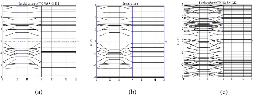
Fig. 4: Band structure plot of (a) Hexagonal TiC NW R=2 (b) Hexagonal TiC NW R=3 and (c) Hexagonal TiC NW R=4.
Puspa Raj Adhikari et al./ BIBECHANA 16 (2019) 7-14 : RCOST p. 13 (Online Publication: Dec., 2018)
4. Conclusions
To study the comprehensive structural and electronic characterization of TiC nanowire, we have calculated the total energy of each freely relaxed structure of TiC nanowire using quantum mechanical DFT calculation with GGA functional. From which we estimate the binding energy of geometry due to number of atoms present on unit cell. This provides the formation probability of the nanowire as the major product during synthesis. The low diameter structures are less stable than the higher diameter geometry is observed from out binding energy calculation. The semiconducting electronic behavior fot the smaller diameter hexagonal TiC nanowire to metallic transition shows that the nanowire is promising candidate for optical to mechanical purposes. The observed electronic band structure are narrow which again adds the field of application in infrared region. The nanowire in 111 plane deserves its metallic property gaining transition phase from semiconducting state at small geometry shape. This property addressed the states per unit higher energy range become lower for larger structure on going from less number of atom containing geometry. The overall analysis of hexagonal TiC nanowire shows higher stability for higher diameter geometries and the transition of electronic property from semiconducting to metallic on increasing wire diameter is observed.
Furthermore the results presented in this article demonstrates that the ability to manipulate different geometry properties in 1-D semiconductor to metallic nanowires offering future experimental insight into mechanical, optical and electric (I-V) property and their noble application that has not been widely investigated to the date.
Acknowledgements
The authors are thankful to ABV-IIITM Gwalior for providing the infrastructural support to perform the present computation at the Computational Nanoscience and Technology Lab (CNTL). We acknowledge all AMR group members and Hydra Research and Policy Center (HRPC) for valuable technical support to this entire investigation. Finally MOST, Nepal is acknowleged for the partial financial support.
References
[1] X. Feng, K. Shankar, O.K. Varghese, M. Paulose, T.J. Latempa, and C.A. Grimes, Vertically aligned single crystal TiO2 nanowire arrays grown directly on transparent conducting oxide coated glass: synthesis details and applications. Nano letters 8 (11) (2008) 3781-3786. doi.org/10.1021/nl802096a.
[2] T. W. Odom, J.L. Huang, P. Kim and C.M. Lieber, Atomic structure and electronic properties of single-walled carbon nanotubes, Nature 391 (6662) (1998) 62-64. doi.org/10.1038/34145.
[3] J. Li, H. Yu, S.M. Wong, X. Li, G. Zhang, P.G.Q. Lo, and D.L. Kwong, Design guidelines of periodic Si nanowire arrays for solar cell application, Applied Physics.Letter 95 (24) (2009) 243113.
doi.org/10.1063/1.3275798 .
[4] S. Paudel, S. Dandeliya, R. Chaurasiya, A. Srivastava and G.C. Kaphle, Magnetism in zigzag and armchair CuO nanotubes: Ab-initio study, Journal of Magnetism and Magnetic Materials 406 (2016) 8-14.
doi.org/10.1016/j.jmmm.2015.12.081.
[5] S. Iijima and T. Ichihashi. Single-shell carbon nanotubes of 1-nm diameter, Nature 363(6430) (1993) 603.
Puspa Raj Adhikari et al./ BIBECHANA 16 (2019) 7-14 : RCOST p. 14 (Online Publication: Dec., 2018)
[6] A. Splendiani, L. Sun, Y. Zhang, T. Li, J. Kim, C.Y. Chim, G. Galli, and F. Wang. Emerging
photoluminescence in monolayer MoS2, Nano let. 10 (4) (2010) 1271-1275. doi.org/10.1021/nl903868w.
[7] N. I. Kovtyukhova, and T.E. Mallouk. Nanowires as Building Blocks for Self‐Assembling Logic and Memory Circuits, Chemistry-A European Journal 8 (19) (2002) 4354-4363. doi.org/10.1002/1521-3765(20021004)8:19<4354::AID-CHEM4354>3.0.CO;2-1.
[8] W. M. Weber, L. Geelhaar, A.P. Graham, E. Unger, D.S. Duesberg, M. Liebau, W. Pamler, C. Cheze, H. Riechert, P. Lugli and F. Kreupl, Silicon-nanowire transistors with intruded nickel-silicide contacts, Nano lett. 6(12) (2006) 2660-2666. doi.org/10.1021/nl0613858.
[9] V. Salgueiriño‐Maceira, M.A. Correa‐Duarte, M. Bañobre‐López, M. Grzelczak, M. Farle, L.M. Liz‐
Marzán, and J. Rivas. Magnetic properties of Ni/NiO nanowires deposited onto CNT/Pt nanocomposites, Adv. Funct. Matt. 18(4) (2008) 616-621. doi.org/10.1002/adfm.200700846.
[10] A. Dey, S. De, A. De and S. K. De. Characterization and dielectric properties of polyaniline–TiO2 nanocomposites, Nanotechnology 15 (9) (2004) 1277. doi.org/10.1088/0957/4484/15/9/028/meta.
[11]Z. Zhang, T. Murayama, M. Sadakane, H. Ariga, N. Yasuda, N. Sakaguchi, K. Asakura and W. Ueda, Ultrathin inorganic molecular nanowire based on polyoxometalates. Nature communications 6 (7731) (2015) 1-10. doi.org/10.1038/ncomms8731.
[12]F. W. Smith and J. Hashemi, Foundations of materials science and engineering. 5th edi. McGraw-Hill
education Europe, London, 2011.
[13]J. G. P. Binner, N. A. Hassine and T. E. Cross, The possible role of the pre-exponential factor in explaining the increased reaction rates observed during the microwave synthesis of titanium carbide, Journal of Materials Science 30 (21) (1995) 5389-5393. doi.org/10.1007/BF00351548.
[14]O. N. Doǧan, J. A. Hawk, J. H. Tylczak, R. D. Wilson and R.D. Govier, Wear of Titanium Carbide reinforced metal matrix composites, Wear 225 (2), (1999) 758-769. doi.org/10.1016/S0043-1648(99)00030-7.
[15]M. Rahman, Z.G. Wang and Y.S. Wong. A review on high-speed machining of titanium alloys, JSME International Journal Series C Mechanical Systems 49 (1) (2006) 11-20. doi.org/10.1299/jsmec.49.11.
[16]A. N. Enyashin and A. L. Ivanovskii, Structural and electronic properties of the TiC nanotubes: Density functional-based tight binding calculations, Physica E: Low-dimensional Systems and Nanostructures 30(1) (2005) 164-168. doi.org/10.1016/j.physe.2005.08.004.
[17]K. Huo, Y. Hu, Y. Ma, Y. Lü, Z. Hu, and Y. Chen. Synthesis and field emission properties of Titanium Carbide nanowires. Nanotechnology 18(14) (2007) 145615. doi.org/10.1088/0957-4484/18/14/145615.
[18]L. C. Voon, Y. Zhang, B. Lassen, M. Willatzen, Q. Xiong and P.C. Eklund, Electronic properties of semiconductor nanowires. Journal of nanoscience and nanotechnology, 8(1) (2008) 1-26.
doi.org/10.1166/jnn.2008.N03.
[19]J. L. Hudgins, G.S. Simin, E. Santi, and M.A. Khan. An assessment of wide bandgap semiconductors for power devices, IEEE Transactions on Power Electronics, 18 (3) (2003) 907-914.
doi.org/10.1109/TPEL.2003.810840.