R E S E A R C H
Open Access
Chaos-based true random number
generators
Luis L Bonilla
*, Mariano Alvaro and Manuel Carretero
*Correspondence: [email protected]
Gregorio Millán Institute for Fluid Dynamics, Nanoscience and Industrial Mathematics, Universidad Carlos III de Madrid, Avenida de la Universidad 30, Leganés, 28911, Spain
Abstract
Random number (bit) generators are crucial to secure communications, data transfer and storage, and electronic transactions, to carry out stochastic simulations and to many other applications. As software generated random sequences are not truly random, fast entropy sources such as quantum systems or classically chaotic systems can be viable alternatives provided they generate high-quality random sequences sufficiently fast. The discovery of spontaneous chaos in semiconductor superlattices at room temperature has produced a valuable nanotechnology option. Here we explain a mathematical model to describe spontaneous chaos in semiconductor superlattices at room temperature, solve it numerically to reveal the origin and characteristics of chaotic oscillations, and discuss the limitations of the model in view of known experiments. We also explain how to extract verified random bits from the analog chaotic signal produced by the superlattice.
Keywords: random bit generator; semiconductor superlattice; deterministic and stochastic chaos
1 Background
Generation of random numbers at high speed is at the core of many activities of economic importance. Online gambling, finance, computer telecommunications, online commerce and data encryption systems, [–], stochastic modeling [], and Monte Carlo simula-tions [] among many others, rely on fast random number generators (RNGs). We also talk about random bit generators (RBGs) when emphasizing that binary numbers are pro-duced. Usually, these generators are based on numerical algorithms that produce seem-ingly unpredictable number sequences. The generator is a function whose input is a short random seed, and whose output is a long stream which is indistinguishable from truly random bits. Such numerical strings yield the keys for secure storage and transmission of data. This conventional approach is cheap and fast, as it is limited only by the proces-sor speed. However, the number sequences thus produced are only pseudorandom, as two identical programs that begin at the same state will produce the same sequence. Then vul-nerability in the pseudorandom number generator (PRNG) may follow, as it famously was the case for Microsoft Windows operating system secure encryption several years ago []. To get cryptographically secure PRNGs, it is convenient to have generated truly ran-dom numbers that may be obtained ideally from inherently ranran-dom or unpredictable pro-cesses. Deterministic processes that are difficult to predict have been used in gambling
since antiquity. For instance, the mechanics of coin tossing shows that small uncertainties in the initial condition ensure equal probability of heads and tails provided some parame-ter (e.g., initial velocity) is large enough [, ]. Similar analyses apply to the case of rolling dice, card shuffling or spinning a roulette wheel. An obvious drawback of these mechani-cal methods is that they are too slow for practimechani-cal use. Other physimechani-cal sources of entropy are too sensitive to external influences and lack robustness, for example, thermal noise or electrical noise in diodes and resistors. These physical processes yield a low analog signal and are easily affected by disturbances including temperature fluctuations. More robust systems are based on quantum mechanical uncertainty, e.g., on whether a photon is de-tected, but they are limited to relatively low rates of number generation (tens of Mb/s) [, ]. Recently, fast generation of truly random numbers (tens or hundreds of Gb/s) has been achieved using chaotic semiconductor lasers [–] and superlattices []. In both cases, quantum fluctuations are amplified by chaotic dynamics to a macroscopic fluctu-ating signal. This signal can be detected by using conventional electronics that is much faster than optical photon counting detectors. While semiconductor lasers require a mix-ture of optical and electronic components, semiconductor superlattices are all electronic submicron devices that can be integrated in more complex circuits. As of now, these two types of devices have been shown to reliably produce truly random sequences of numbers at fast rates in laboratory experiments. If they show to be scalable, these devices could be vastly useful, as the performance and reliability of our digital networked society relies on the ability to generate fast and cheaply large quantities of random numbers.
In this paper, we comment the possible use of spontaneously chaotic semiconductor superlattices (SLs) as true random number generators. In Section , we discuss the math-ematical model for a single SL under voltage bias. The model consists of a number of coupled stochastic differential equations together with algebraic boundary and voltage bias conditions. In Section ., numerical solutions of the model equations show that the thermal and shot noises existing in the SL enhance stable spontaneous chaos in voltage intervals where the corresponding deterministic model exhibits chaos. The noises also induce chaos in nearby voltage intervals where the deterministic system had periodic os-cillations. We also discuss the relation of our results to experiments and which features of the model need to be revised in order to optimize the chaotic oscillations. In Section . and following Ref. [], we explain how to obtain a high-speed true random bit generator by processing the chaotic current oscillations provided by the device. Section summa-rizes our findings and perspectives for fast random bit generators based on semiconductor superlattices. Two Appendices provide details on the derivation of the model equations.
2 Mathematical model and methods for a single superlattice
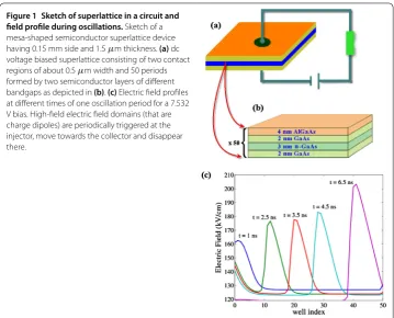
Figure 1 Sketch of superlattice in a circuit and field profile during oscillations.Sketch of a mesa-shaped semiconductor superlattice device having 0.15 mm side and 1.5μm thickness.(a)dc voltage biased superlattice consisting of two contact regions of about 0.5μm width and 50 periods formed by two semiconductor layers of different bandgaps as depicted in(b).(c)Electric field profiles at different times of one oscillation period for a 7.532 V bias. High-field electric field domains (that are charge dipoles) are periodically triggered at the injector, move towards the collector and disappear there.
miniband width strongly decreases []. In the limit of infinite wavenumber times width, the miniband widths vanish and the spectrum corresponds to that of an isolated quantum well (QW). Superlattices with wide (narrow) minibands are said to be strongly (weakly) coupled []. Superlattice layered materials are now routinely grown by molecular beam epitaxy as wafers that are then processed into a number of cylindrical mesas of very large circular or square section ( to microns are the typical radii or sides). Contact re-gions are attached to the ends of the SL that are then integrated in a circuit, as sketched in Figure (a).
SLs were proposed in by Esaki and Tsu to develop a device that exhibits Bloch os-cillations []. Although such osos-cillations were observed in experiments years later [], no practical device using them has been so far developed. Instead, SLs have been used to build gigahertz oscillators for communications purposes, detectors for terahertz sig-nals or infrared radiation and quantum-cascade lasers commercially used for a variety of purposes, such as environmental sensing and pollution controlling, industrial processes control (e.g., combustion control, converter diagnosis, collision avoiding radar in automo-tive industry), medical applications (breath analysis, early detection of ulcers), etc. []. In , experiments demonstrated the existence of spontaneously chaotic oscillations of the current through a SL at room temperature under voltage bias, as in the sketch of Fig-ures (a) and (b) []. This paved the way to using SLs as true random number generators [].
the case of strongly coupled SLs [, ], but none so far for weakly coupled SLs, as those displaying spontaneous chaos in experiments [, ]. The main reason for this failure is that Boltzmann-type equations for SLs are based on electrons populating minibands at zero electric field, and such a picture is far from reality in the presence of electric fields that are sufficiently strong:eFl>, where –e< is the electron charge, –F the electric
field,lthe SL period andis the miniband width [].
2.1 Model
For chaotic phenomena in weakly coupled SLs,eFl, and different modeling is called
for. One key observation is that the miniband widths are small compared with the broaden-ing of the energy levels due to scatterbroaden-ing,/τsc, and to the typical values of the electrostatic
energy per SL period,eFl. Thus, the escape time from a QWτesc∼l/vM∼/(vMandFM are typical electron velocities and electric fields during oscillations) is much larger than the scattering time,τsc. This implies that the electron distribution in the wells is in local
equilibrium []. Moreover, the dielectric relaxation timeτdi∼Nldi/vM∼NεFMτesc/(eND)
(εis the SL dielectric constant,NDis the two-dimensional (D) doping density, andNis
of the order of the number of SL periods), in which the current density across the SL re-acts to sudden changes in the electric field profile, is typically larger than the escape time. Therefore, we can assume that the tunnelling current density between quantum wells is stationary on the longer time scale of the dielectric relaxation time []. A minimal the-ory of charge transport in weakly coupled SLs should therefore specify (i) which slowly varying magnitudes characterize the local equilibrium distribution function in the wells (at least the electric field and the electrochemical potential or the electron density), (ii) the equations relating these magnitudes (e.g. the charge continuity and the Poisson equation) and (iii) how to close these equations by calculating the necessary relations between mag-nitudes (e.g. the stationary tunnelling current between adjacent wells). In our simulations, we have added intrinsic noise to the usual sequential tunneling model of electron
trans-port in a weakly coupledn-doped SL [, , ]
εdFi+Ji→i+dt+
ξidWi=J(t)dt, ()
Ji→i+= eni
l v (f)(F
i) –Ji→i– +(Fi,ni+,T), ()
ni=ND+ ε
e(Fi–Fi–). ()
Herei= , . . . ,N(N= is the number of SL periods []) and the Ito stochastic differ-ential equations () are current balance (Ampère) equations. Together with the Poisson equation (), they ensure charge continuity, as time differentiation of () and use of () yield
edni= [Ji–→idt+
ξi–dWi–] – [Ji→i+dt+
ξidWi]. ()
The D electron densityniis given by the Poisson equation (), in which the equivalent D
doping density due to the doping of the central part of the QW isND= ×cm–.Ji→i+, √
welliand the D electron densities in the corresponding wells,niandni+, according to
the formulas [, ]
Ji→i– +(Fi,ni+,T) =
em∗kBT πl v
(f)(F
i)ln
+e–kBTeFile πni
+
m∗kBT – , ()
v(f)(Fi) = n
j=
l(γ
C+γCj)
m∗ Ti(C)
(C–Cj+eFil)+ (γC+γCj)
, ()
Ti() = k
iki+αi(ki+αi)–(ki++αi)– (dW+α–i–+α–i )(dW+αi–++αi–)eαidB
, ()
ki=
√
m∗, ki+=
m∗(+elFi), ()
αi–=
m∗ eVB+e
dB+
dW
Fi–
, ()
αi=
m∗ eVB–
edWFi
–
, ()
αi+=
m∗ eVB–e
dB+
dW
Fi–
. ()
These formulas are obtained by writing the electron Hamiltonian as a sum of eigenstates of the electron in each QW plus a small term that expresses the possible motion from one QW to its adjacent wells by tunneling across the barrier separating them; see Appendix and Ref. []. Then the tunneling current density is obtained by first-order perturbation theory in the tunneling term and use of the transfer Hamiltonian method [, ]. The inte-grals appearing in the tunneling current are further approximated by asymptotic methods as explained in Appendix A of Ref. []. The forward velocityv(f)(F
i) is a function given in
[, , ] with peaks corresponding to three energy levelsECjat , , and meV
calculated by solving a Kronig-Penney model for the SL configuration of References [, , ]. The level broadenings due to scattering,γCj, are ., and meV, respectively, for the three energy levels []. The energy barrier in the absence of potential drops,eVB,
depends on the fractionxof Al in the barriers,x= . for the SLs of Refs. [, , ].
In this paper, we have usedeVB= meV. Alsom∗= (. + .x)me= .me(for
x= .),me,dB= nm,dW= nm,l=dB+dW,ε=l/[dεWW +
dB
εB],εB= .,εW= .,
,kB, andT, are the effective electron mass, the electron mass in vacuum, the (Al, Ga)As
barrier thickness, the GaAs well thickness, the SL period, the SL permittivity, the barrier permittivity, the well permittivity, the dielectric constant of the vacuum, the Boltzmann constant, and the lattice temperature, respectively.
The coefficients of the independent identically distributed Brownian motionsdWiin ()
resulting formula is:
ξi=
e A
ev(f)(F
i)
l ni+J –
i→i+(Fi,ni+,T)
+em
∗k BT πl v
(f)(F
i)
e–kBTeFil(e πni
m∗kBT – )
+e–kBTeFil(e πni
m∗kBT – )
, ()
in whichA=sis the SL cross section of a square mesa with sides= μm. The current
density at the contacts and the voltage bias condition are
J→=σF, JN→N+=σ nN
Nc
FN, ()
N
i= Fi=
V+η(t)
l . ()
HereV is the dc voltage,η(t) is a fluctuation due to the voltage source andσ andNc
are the contact conductivity, and the equivalent D doping density of the anode region, respectively [].
The mathematical model we use has some limitations that may have to be overcome in more precise future studies. It corresponds to an idealized SL in which all periods have identical values ofdW,dB,ND, andVB. The effective massm∗ and permittivityεare the same irrespective on whether they correspond to a barrier or a well. In addition, the model does not include D effects due to imperfect growth: barrier and well widths may vary in the SL cross section perpendicular to the growth direction. Some of these effects were addressed in [].
2.2 Methods
We have solved the stochastic model given by Eqs. ()-() withη(t) = (internal noise
only) for the SL of Refs. [, , ] at K using a standard stochastic Euler-Maruyama method (explicit Euler method corresponding to Ito integration) []. Coding of the nu-merical method follows the indications in Ref. []. To calculate the largest Lyapunov ex-ponent (LLE), we have simultaneously integrated all perturbed and unperturbed
trajecto-ries during , ns and used the Benettinet al.algorithm [] with a renormalization
period of ns. LLE calculations with the Gaoet al.algorithm [] give similar results.
3 Results and discussion
3.1 Spontaneous chaotic oscillations
Figure 2 Mean current, largest Lyapunov exponent and Fourier spectrum in terms of voltage. (a)Mean current and largest Lyapunov exponent vs voltage, and(b)Fourier spectrum vs voltage for the second oscillatory interval. The inset in panel(a)shows the mean current for a larger voltage interval and the vertical arrows mark supercritical Hopf bifurcation points bounding the second oscillatory voltage interval. Without noise, the voltage interval of spontaneous chaos is very narrow (3 mV width) and the LLE is only 0.25. Internal noise increases the LLE up to 0.76 and widens to 30 mV the voltage range for spontaneous chaos.
room temperature, wave fronts are not sharp, and spontaneous chaos arises due to other reasons, as explained in Ref. [] and in what follows.
.. Internal noise induces and enhances chaos
We have found self-sustained oscillations in two voltage intervals that appear as plateaus in the SL current-voltage characteristics, forV< (EC–EC)/eand forV> (EC–EC)/e. At
the left end of both intervals, small-amplitude current oscillations appear as supercritical Hopf bifurcations from the stationary state. They are caused by the repeated creation of field pulses that dissolve before arriving at the collector. The range of voltages for which this behavior is observed is much narrower on the first voltage interval than on the second one. On both voltage intervals, oscillations die via supercritical Hopf bifurcations. The reverse tunneling currentJi→i– + given by () is much larger for the smaller fields at the first voltage plateau than for the larger fields at the second plateau. The internal noise is correspondingly larger compared with the mean current at the first plateau. Spontaneous chaotic oscillations in the first voltage interval were discussed in Ref. []. Here we shall present similar results obtained for voltages on the second plateau.
Figure 3 Characterization of chaotic oscillation. (a)Current and(b)density plot of the electric field vs time, showing how the dipole occasionally fails to reach the receiving contact;(c)Fourier spectrum of the current;(d)phase diagram of the electric field (in kV/cm) at wells 45 and 46, showing how the chaotic oscillations fill a mussel-shaped region;(e)multifractal dimension. Applied voltage: 7.3513V.
of Figure (c) and to the confined dipole motion, respectively. Just after the mean current peak in Figure (a), there is a voltage interval of positive LLE that indicates sensitivity to initial conditions characteristic of a chaotic attractor.
Figure (a) shows that the LLE is positive in a narrow voltage interval of the determin-istic system. Internal noise both widens this interval and increases the LLE. At voltage values for which the LLE is positive for the stochastic system but not for the determin-istic system, noise induces chaos. At voltages for which the determindetermin-istic system has a positive LLE, noise enhances chaos, something already demonstrated for simple dynami-cal systems [, ]. This picture is confirmed by examining the chaotic attractor. At the voltage marked in Figure (a) corresponding to the maximum value of the LLE, the
fluc-tuations create a mussel-shapedmultifractalchaotic attractor out of the above mentioned
and the density plot in Figure (b) show that shorter time separations between two large spikes correspond to the formation of a dipole that dissolves before reaching the collector. Longer separations between consecutive large spikes correspond to a dipole that reaches the collector, as in Figure (c). Thus, two different oscillation modes are observable in the chaotic attractor: injector-to-collector dipole motion and dipole motion from injector to premature annihilation inside the SL. The latter corresponds to the well-to-well hopping mode postulated in Ref. []. The inter-spike intervals are similar but never repeat them-selves and tend to produce a mussel-shaped attractor in the phase plane of the field at two adjacent wells as depicted in Figure (d). Noise increases the multifractal dimension
Dqof the deterministic attractor as shown in Figure (e). In Figure (a), the mean
oscil-lation amplitude (understood as difference between the peak and the valley currents) is
∼ mA, the mean interspike interval is∼. ns, and there are large peaks in a ns
time interval. Our values are quite close to those observed in the experiments, ∼ mA
mean oscillation amplitude and∼. ns mean interspike interval, with large spikes in a
ns interval []. What is the role of fluctuations in the creation of spontaneous chaos? Without noise, the LLE reaches a maximum value of . in a narrow voltage interval, whereas the fluctuations widen this interval and enhance the LLE up to .. The internal noise due to fluctuations of the current enhances spontaneous chaos, increases its fractal dimension and induces chaos in voltage regions adjacent to those of purely deterministic chaos. Voltage fluctuations widen the voltage interval of spontaneous chaos.
.. Comparison with experiments
Experiments [, , ] show that oscillations appear for voltages on the first plateau and that they have frequencies about . times larger than those predicted by simulations of our mathematical model []. The current spikes observed in experiments are more ir-regular than those appearing in simulations. These features of oscillations observed in experiments point to the presence of imperfections not taken into account in the model. In earlier work on the role of imperfections [], numerical simulations of a related dis-crete model showed that a % fluctuation in doping density could increment by a factor of the oscillation frequency. Obvious imperfections that should be taken into account in our model include: (i) fluctuations of the doping density, (ii) fluctuations indBanddW,
(iii) fluctuations inVB. Once imperfections are included in the mathematical model, we
can pose the objective ofoptimizing chaos, i.e., introducing intentional imperfections so
as to widen the voltage intervals for which there are chaotic oscillations, and increase the LLE and the complexity of attractors. These features would increase the usefulness of the device as a true random number generator.
3.2 Random Bit Generation from chaotic oscillations
There are a number of ways to obtain a RBG out of a chaotic signal. In this section, we
will explain the methods used by Liet al.[], using one of the figures they extracted from
experimental measurements.
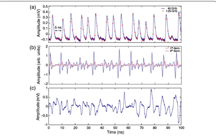
Figure 4 Analog to digital conversion of chaotic signal. (a)A 100 ns trace of experimentally observed chaotic oscillations, digitized at 40 GHz (blue line) and 1.25 GHz (red circles).(b)1st and 4th order discrete derivatives of the SL oscillations sampled at 1.25 GHz and presented in panel(a).(c)Linear combination of 4 recorded superlattice oscillation traces, digitized at 40 GHz. Taken from [15] with permission. Material copyrighted by the American Physical Society.
bit sequence. To overcome this limitation, we may calculate a high order derivative to mix data sampled in a window between large peaks with nearby random spikes. For the case of a . GHz sampling rate, the th discrete derivative mixes data from
consecu-tive measurements which are separated by= . ns, at timest,t–,t– ,t– ,
andt– . Hence, each derived data point used for the generation of the random bit
se-quence mixes ns of information, which is close to the average period of the oscillation ( ns), as indicated in Figure (a). Thus this time window includes, with a high probability, combined data taken from a chaotic current peak and the interval between large peaks. Figure (b) shows the st and th derivatives of the signal in Figure (a), sampled at . GHz. Whereas for the st derivative many points have values near zero, the th derivative values fluctuate at all time scales and it has a number of peaks comparable to the number of large peaks in Figure (a).
The generation of the random bit stream from the chaotic consists of the following two
steps. First, we calculate thenth derivative usingn+ successive values of the recorded
signal. Second, we append themleast significant bits (LSBs) of the results of thenth deriva-tive to the bit sequence. Recall that the LSBs are the most sensideriva-tive to small fluctuations.
Using n= and retainingm= LSBs out of bits, truly random bits are generated at
. Gbit/s using a sampling rate of . GHz []. For higher sampling rates, larger
val-ues ofnare needed to achieve verified randomness using the NIST statistical test suite
SL – SL of four uncorrelated traces of the chaotic signal, digitized at GHz. Liet al.
obtained a Gbit/s RBG with verified randomness using such a linear combination, a GHz sampling rate and LSBs. They obtained a faster rate verified RBG by combining signals and a faster sampling rate. See [] for details.
4 Conclusions
The discovery of fast spontaneous chaotic oscillations of the current through semicon-ductor superlattices at room temperature brings to light their possible applications as true random bit generators []. Fast true random bit generators coming from tiny submicron all-electronic devices could be invaluable in secure communications and data storage. In
this paper, we have discussed a mathematical model to describe spontaneous chaos in
ide-alizedsuperlattices with identical wells and barriers. Our numerical simulations show that spontaneous chaos possibly may appear directly from a two-frequency quasiperiodic at-tractor. We have also shown that the unavoidable shot and thermal noises existing in the nanostructure both enhance existing deterministic chaos (increasing its fractal dimen-sion and largest Lyapunov exponent) and induce chaos in nearby voltage intervals. We have discussed that the differences between numerical and experimental results may be due to imperfections in the doping density, the gallium content in the barriers, and the size thereof. A better model needs to be developed to discuss the imperfections and their effect in the chaotic oscillations: ideally we could tune chaos via the introduction of con-trolled imperfections. We also explain how to extract verified random bit generators from a chaotic signal by digitalization and extraction of least significant bits from high order numerical derivatives, or by combining several chaotic signals coming either several su-perlattices or from far apart segments of the same long chaotic signal.
Appendix 1: Derivation of deterministic tunneling currents
We use the methods of Ref. []. The tunneling Hamiltonian is
Htotal=H+HT= N+
i= Hi+
N
j=
HTj, (A.)
Hi=
ki
Eikic
†
ikiciki, HTj=
kjkj+
Tkjkj+c
†
j+kj+cjkj+H.c.
. (A.)
Here the Hamiltonian H is a sum of individual Hamiltonians for each QW or contact
and assumes that they are uncoupled from one another. H.c. stands for the Hermitian conjugate of the preceding term. The unperturbed single-electron states have absolute
energies denoted byEikimeasured from the conduction band edge in the emitter contact.
The operatorsc†ikiandcikidenote creation and annihilation operators for electrons in the
ith well or contact with three-dimensional wave vector kiand satisfy standard fermionic
commutation rules:{ciki,cjkj}=cikicjkj+cjkj,ciki= ,{c
† iki,c
†
jkj}= ,{ciki,c
†
jkj}=δijδkikj. Each
QW contains a set ofnsubbands and its Fermi energy measured from the conduction
band edge in the emitter contact iswi.HTis a small perturbation ofHrepresenting the
The change of the electron operator number at theith well,Ni=
kic
†
ikiciki, is related to the tunneling current operatorJˆi→i+by
eN˙i=
i
[Htotal,eNi] =
i
[HTi–,eNi] –
i
[HTi,eNi] =Jˆi–→i–Jˆi→i+. (A.)
In the interaction representation, we haveHT(t) =eiHt/HTe–iHt/andˆJi→i+(t) =eiHt/× ˆ
Ji→i+e–iHt/and the average tunneling current density satisfies the Kubo formula []
Ji→i+(t) =
t
–∞ ˆ
Ji→i+(t),HT
tdt. (A.)
Here the average is over the thermodynamic local equilibria at the QWs i and i+ .
A straightforward lengthy evaluation yields
Ji→i+(t) =
πe
kjkj+
|Tkjkj+|
δ(E
j+kj+–Ejkj)
×nF(Ej+kj+–wj+) –nF(Ejkj–wj)
, (A.)
wherenF(x) = /( +ex/kBT) is the Fermi distribution function. Here the overall energy at the jth QW isEjkj =+E⊥,E⊥=
k
⊥/(m∗), in which is the energy at the well, and
k⊥ comprises the components of the wave vector that are orthogonal to the SL growth
direction. The matrix element:
Tkjkj+=
m∗
A
ψj∇ψj∗+–ψj∗+∇ψj
·dA, (A.)
is calculated by using Bardeen’s Transfer Hamiltonian method [, ]. The wave
func-tions of two adjacent square QWs,ψjandψj+, are approximated by those of free
parti-cles in two isolated wells separated by an infinitely thick barrier. Then continuity of wave functions and their derivatives are used to find out the coefficients of the wave function ex-pressions in different space intervals and the resulting wave functions produce the matrix element (A.) []. The result is []
|Tkiki+|
= π
m∗Bi–,iBi,i+Tiδk⊥k⊥, Bi,i+=
ki+ dW+α–i +αi–+
, (A.)
where the transmission coefficient through a thick barrier is
Ti() =
k
iki+αi (k
i +αi)(ki++αi)
e–αidB. (A.)
In (A.) and (A.), we have used the definitions
ki=
m∗(+eWi), (A.)
αi=
m∗e VB–Wi–
Vwi
–
e
Wi=
e +V+
i–
j=
(Vj+Vwj) +
Vwi
. (A.)
We now transform the sums in (A.) to integrals over the energiesEjkj=+E⊥using a
broadened spectral density to account for scattering. If the latter depends only on, we
obtain
Ji→i+= e
m∗
n
j=
dAiC()AiCj+()Bi–,i()Bi,i+()Ti()
×
dE⊥
+e(+E⊥–wi)/k
BT
+
+e(+E⊥–wi+)/kBT
. (A.)
Here the broadened spectral function is
AiCν() =
γCν
π
(–Ciν)+γ
Cν
, (A.)
whereγν=/τsc, withτscbeing the lifetime associated to the dominant scattering
pro-cesses (interface roughness, impurity scattering, phonon scattering, etc.). The relation
be-tween the local Fermi energy and the electron density at theith well is obtained from
ni=
m∗kBT π
AiC()ln +e
wi–
kBT d. (A.)
Integrating now (A.) overE⊥, we obtain
Ji→i+= ekBT πm∗
n
j=
ACi()ACji+()Bi–,i()Bi,i+()Ti()
×ln +e
(wi–)/kBT
+e(wi+–)/kBT
d. (A.)
In (A.) all energies are measured from the conduction band edge in the emitter contact.
Notice that the complicated dependence of the wave vectorskiandαiwith the potential,
Wi, may be transferred to the Fermi energies by changing variables in the integrals of the
system (A.) so that the lower limit of integration (the bottom of theith well) is zero:
=+eWi. Then the resulting expressions have the same forms as Eqs. (A.) and (A.)
ifiC,iCj+, andwiin them are replaced by
C=Ci+eWi, (A.)
μi≡wi+eWi, (A.)
respectively.Wiis given by (A.). The integrations now go from= to infinity. Notice
thatCjis independent of the well indexiprovided we assume that the energy level drops
half the potential drop for the whole welleVwiwith respect to its position in the absence of bias. Equation (A.) becomes
ni(μi) =
m∗kBT π
∞
AC()ln
+e
μi–
HereAC() is obtained by substitutingC(the energy of the first subband measured from
the bottom of a given well, therefore independent of electrostatics) instead ofCiin (A.).
Notice that (A.) defines a one-to-one relation betweenniandμiwhich is independent
of the indexior the potential drops. The inverse functionμi=μ(ni,T) gives the
chemi-cal potential or free energy per electron. This is theentropicpart of the electrochemical
potential (Fermi energy)
wi=μ(ni,T) ––eV–e
i–
j=
(Vj+Vwj) –
eVwi
. (A.)
According to (A.), the Fermi energy,wi (electrochemical potential), is the sum of the
electrostatic energy at theith well, ––eV–e i–
j=(Vj+Vwj) –eVwi/, and the chemical potential,μi=μ(ni,T). After the change of variable in the integrals, the wave vectors in (A.) become:
ki=
√
m∗,
αi=
m∗
eVB–
eVwi
–
,
ki+=
m∗
+eVi+e
Vwi+Vwi+
,
αi–=
m∗
eVB+
eVwi
+eVi––
,
αi+=
m∗
eVB–
eVwi
–eVi–eVwi+–
,
(A.)
where now= at the bottom of theith well. This shows that the tunneling current
den-sity,Ji,i+, in (A.) is a function of: the temperature,μiandμi+(therefore ofniandni+),
the potential dropsVi,Vi+,Vwi, andVwi+. The potential drops are related to the electron density through the discrete Poisson equations
εVwi
dW
=εVi–
dB
+e(ni–ND)
, (A.)
εVi
dB =εVi–
dB
+e(ni–ND), (A.)
from which
Vwi=dW
Vi+Vi–
dB
. (A.)
To obtain simpler expressions for the tunneling current density, we assume that Vi/dB
andVi±/dB are approximately equal to an average fieldFi. Then Vwi=dWFi according to (A.). This assumption departs from the previous approximations and yields a new model. The point of contact with our previous results is thatAC()ACj(+eVi+e[Vwi+
Vwi+]/) is the controlling factor in the expressions forv(f) andJ
–
i→i+ (the transmission
contributing most to the integral). This controlling factor is uniquely determined by the potential dropVi+ (Vwi+Vwi+)/≈(dW+dB)Fi=Fil. Then the wave vectorski,αi, etc. become the expressions in ()-(). If the Lorentzian functions (A.) are sharp enough (γCν→),
ni=
m∗kBT π ln
+e
μi–C
kBT , (A.)
in (A.) and we may keep only the product of two Lorentzian functions inside the integral (A.), and approximate all other functions by their values at=C(=iC). Then ()
and () are obtained; see also Appendix A of [].
Appendix 2: Stochastic current
The stochastic currents have two components: shot (partition) noise of Poisson type and thermal noise. The shot noise appears because it is really single electrons that tunnel
through barriers and there is a largeintegernumber of electrons, whereas the tunneling
current deals with real-valued electron densities, not with integer multiples of electron charge divided by surface area. The difference constitutes shot noise. For the large values of the barrier cross section area, Poissonian statistics of the shot noise is appropriate [], and thus its correlation is proportional to the terms of the tunneling current (). This pro-duces the first two terms in () according to [, ]. To derive the correlation due to thermal noise, we first write () as
Ji→i+= eni
l v (f)(F
i) –Ji→i– +(Fi,ni,T)
–Ji→i– +(Fi,ni+,T) –Ji→i– +(Fi,ni,T)
. (B.)
The two last terms in (B.) form a discrete diffusive term,
Ji→idiff+=Ji→i– +(Fi,μi+,T) –Ji→i– +(Fi,μi,T)
=D+μ
Ji→i– +(Fi,μi,T)
, (B.)
in which, using (A.), we have written that the tunneling current depends on the chemical potential instead of the electron density. Then
Ji→i– +(Fi,μi+,T) =
em∗kBT πl v
(f)(F
i)ln
+e
μi+–eFil–C
kBT . (B.)
After linearization, the discrete diffusive current (B.) becomes
δD+μJi→i– +(Fi,μi,T)
=∂J
–
i→i+
∂μi
D+μ(δμi). (B.)
According to fluctuating hydrodynamics, there is a zero mean white noise ηi(t)
corre-sponding to the diffusive current whose correlation is [, ]:
ηi(t)ηjt= ekBT ∂J–
i→i+
∂μi δij
Aδ
t–t
=e
m∗k BT πAl
v(f)(F
i)e
μi–C–eFil kBT
+e
μi–C–eFil kBT
δijδ
This contributes the last term to () after we replace ni instead of μi by means of (A.).
It turns out that the numerical simulations of the stochastic model are not that sensi-tive to the particular expressions derived in this Appendix. Terms of the same order of magnitude produce very similar results.
Abbreviations
RNG, RBG, PRNG, SL, QW, LLE, LSB
Competing interests
The authors declare that they have no competing interests.
Authors’ contributions
LLB wrote the paper, proposed the model and directed the investigation. MA and MC solved numerically the model equations. All authors discussed the results and their interpretation in equal share.
Authors’ information
LLB is a Professor of Applied Mathematics and director of the Institute. He has done research work on modeling, analysis, interpretation and validation of nonlinear charge transport in semiconductor superlattices and other nanostructures since 1994. He co-proposed discrete models widely used in this field, wrote review articles and one related book. MC is Associate Professor of Applied Mathematics and MA is a Lecturer and both are members of the Institute. They have been working in this field since the 2000s, with particular expertise in the numerical solutions of ordinary, partial and stochastic differential equations. The authors collaborate regularly with experimental physicists working on these topics.
Acknowledgements
This work has been supported by the Spanish Ministerio de Economía y Competitividad grants FIS2011-28838-C02-01 and MTM2014-56948-C2-2-P.
Received: 28 January 2016 Accepted: 20 June 2016
References
1. Stinson DR. Cryptography: theory and practice. 3rd ed. Boca Raton: CRC Press; 2006.
2. Gallager RG. Principles of digital communication. Cambridge: Cambridge University Press; 2008.
3. Nielsen MA, Chuang IL. Quantum computation and quantum information. Cambridge: Cambridge University Press; 2000.
4. Asmussen S, Glynn PW. Stochastic simulation: algorithms and analysis. New York: Springer; 2007.
5. Binder K, Heermann DW. Monte Carlo simulation in statistical physics. An introduction. 4th ed. Berlin: Springer; 2002. 6. Dorrendorf L, Gutterman Z, Pinkas B. Cryptanalysis of the random number generator of the windows operating
system. ACM Trans Inf Syst Secur 2009;13(1):10. doi:10.1145/1609956.1609966. 7. Keller JB. The probability of heads. Am Math Mon. 1986;93:191-7.
8. Diaconis P, Holmes S, Montgomery R. Dynamical bias in the coin toss. SIAM Rev. 2007;49(2):211-35.
9. Dynes FJ, Yuan ZL, Sharpe AW, Shields AJ. A high speed, postprocessing free, quantum random number generator. Appl Phys Lett. 2008;93:031109.
10. Comandar LC, Fröhlich B, Lucamarini M, Patel KA, Sharpe AW, Dynes JF, Yuan ZL, Penty RV, Shields AJ. Room temperature single-photon detectors for high bit rate quantum key distribution. Appl Phys Lett. 2014;104:021101. 11. Uchida A, Amano K, Inoue M, Hirano K, Naito S, Someya H, Oowada I, Kurashige T, Shiki M, Yoshimori S, Yoshimura K,
Davis P. Fast physical random bit generation with chaotic semiconductor lasers. Nat Photonics. 2008;2:728-32. 12. Murphy TE, Roy R. The world’s fastest dice. Nat Photonics. 2008;2:714-5.
13. Reidler I, Aviad Y, Rosenbluh M, Kanter I. Ultrahigh-speed random number generation based on a chaotic semiconductor laser. Phys Rev Lett. 2009;103:024102.
14. Kanter I, Aviad Y, Reidler I, Cohen E, Rosenbluth M. An optical ultrafast random bit generator. Nat Photonics. 2010;4:58-61.
15. Li W, Reidler I, Aviad Y, Huang Y, Song H, Zhang Y, Rosenbluth M, Kanter I. Fast physical random-number generation based on room-temperature chaotic oscillations in weakly coupled superlattices. Phys Rev Lett. 2013;111:044102. 16. Bastard G. Wave mechanics applied to semiconductor heterostructures. New York: Halsted Press; 1988. 17. Bonilla LL, Grahn HT. Nonlinear dynamics of semiconductor superlattices. Rep Prog Phys. 2005;68:577-683. 18. Esaki L, Tsu R. Superlattice and negative differential conductivity in semiconductors. IBM J Res Dev. 1970;14:61-5. 19. Feldmann J, Leo K, Shah J, Miller DAB, Cunningham JE, Meier T, von Plessen G, Schulze A, Thomas P, Schmitt-Rink S.
Optical investigation of Bloch oscillations in a semiconductor superlattice. Phys Rev B. 1992;46:7252-5.
20. Huang YY, Li W, Ma WQ, Qin H, Zhang YH. Experimental observation of spontaneous chaotic current oscillations in GaAs/Al0.45Ga0.55As superlattices at room temperature. Chin Sci Bull. 2012;57:2070-2.
21. Cercignani C. Mathematical methods in kinetic theory. New York: Plenum Press; 1969. 22. Markowich PA, Schmeiser CA, Ringhofer C. Semiconductor equations. Vienna: Springer; 1990.
23. Jüngel A. Transport equations for semiconductors. Lecture notes in physics. vol. 773. Berlin: Springer; 2009. 24. Bonilla LL, Escobedo R, Perales A. Generalized drift-diffusion model for miniband superlattices. Phys Rev B.
2003;68:241304.
26. Bonilla LL, Galán J, Cuesta JA, Martínez FC, Molera JM. Dynamics of electric field domains and oscillations of the photocurrent in a simple superlattice model. Phys Rev B. 1994;50:8644-57.
27. Alvaro M, Carretero M, Bonilla LL. Noise enhanced spontaneous chaos in semiconductor superlattices at room temperature. Europhys Lett. 2014;107:37002.
28. Bonilla LL, Escobedo R, Dell’Acqua G. Voltage switching and domain relocation in semiconductor superlattices. Phys Rev B. 2006;73:115341.
29. Xu H, Teitsworth SW. Dependence of electric field domain relocation dynamics on contact conductivity in semiconductor superlattices. Phys Rev B. 2007;76:235302.
30. Bonilla LL. Theory of nonlinear charge transport, wave propagation and self-oscillations in semiconductor superlattices. J Phys Condens Matter. 2002;14:R341-81.
31. Huang YY, Li W, Ma WQ, Qin H, Grahn HT, Zhang YH. Spontaneous quasi-periodic current self-oscillations in a weakly coupled GaAs/(Al, Ga)As superlattice at room temperature. Appl Phys Lett. 2013;102:242107.
32. Blanter YM, Büttiker M. Shot noise in mesoscopic conductors. Phys Rep. 2000;336:1-166.
33. Bonilla LL, Sánchez O, Soler JS. Nonlinear stochastic discrete drift-diffusion theory of charge fluctuations and domain relocation times in semiconductor superlattices. Phys Rev B. 2002;65:195308.
34. Bonilla LL. Theory of charge fluctuations and domain relocation times in semiconductor superlattices. Physica D. 2004;199:105-14.
35. Landau LD, Lifshitz EM. Fluid mechanics. New York: Pergamon Press; 1959.
36. Keizer J. Statistical thermodynamics of nonequilibrium processes. New York: Springer; 1987.
37. Schwarz G, Wacker A, Prengel F, Schöll E, Kastrup J, Grahn HT, Ploog K. The influence of imperfections and weak disorder on domain formation in superlattices. Semicond Sci Technol. 1996;11:475-82.
38. Kloeden PE, Platen E. Numerical solution of stochastic differential equations. Berlin: Springer; 1992.
39. Higham DJ. An algorithmic introduction to numerical simulation of stochastic differential equations. SIAM Rev. 2001;43:525-46.
40. Benettin G, Casartelli M, Galgani L, Giorgilli A, Strelcyn JM. On the reliability of numerical studies of stochasticity. Nuovo Cimento B. 1978;44:183-95.
41. Gao JB, Hwang SK, Liu JM. When can noise induce chaos? Phys Rev Lett. 1999;82:1132-5.
42. Zhang Y, Kastrup J, Klann R, Ploog KH, Grahn HT. Synchronization and chaos induced by resonant tunneling in GaAs/AlAs superlattices. Phys Rev Lett. 1996;77:3001-4.
43. Cantalapiedra IR, Bergmann MJ, Bonilla LL, Teitsworth SW. Chaotic motion of space charge waves in semiconductors under time-independent voltage bias. Phys Rev E. 2001;63:056216.
44. Amann A, Schlesner J, Wacker A, Schöll E. Chaotic front dynamics in semiconductor superlattices. Phys Rev B. 2002;65:193313.
45. Moon H-T. Two-frequency motion to chaos with fractal dimensiond> 3. Phys Rev Lett. 1997;79:403-6. 46. Crutchfield JP, Farmer D, Huberman BA. Fluctuations and simple chaotic dynamics. Phys Rep. 1982;92:45-82. 47. NIST Statistical Test Suite. http://csrc.nist.gov/groups/ST/toolkit/rng/stats_tests.html
48. Zwanzig R. Nonequilibrium statistical mechanics. New York: Oxford University Press; 2001. 49. Bardeen J. Tunneling from a many-particle point of view. Phys Rev Lett. 1961;6:57-9.