Five-Level Full-Bridge Zero Voltage and Zero
Current Switching DC-DC Converter Topology
V. Sivaparvathi SRI. J. Sivavara Prasad
Assistant Professor & M-Tech Associate Professor & M-Tech (Ph. D)
Department of Electrical Engineering Department of Electrical Engineering
Lakireddy Balireddy College of Engineering, Vijayawada, India
Lakireddy Balireddy College of Engineering, Vijayawada, India
Abstract
This project proposes a development of soft switching scheme for Five level DC-DC converter is used to provide zero voltage switching condition for all the controlled switches. In this paper, the gate pulses are generating from PWM controller. This paper describes the main operational modes of the proposed converter as well as simulation results and also observes and compares the switching losses of the proposed converter with and without zero voltage switching scheme.
Keywords: Zero Voltage Switching (ZVS), Zero Current Switching (ZCS)
_______________________________________________________________________________________________________
I.
I
NTRODUCTION TO SQOOPIn ordinary converters there exists many problems like stress on switches, switching losses, EMI etc…. These problems can be eliminated by using ZVS and ZCS converters. In ZVS, the switches are turned on and off at zero voltages and in ZCS, the switches are turned on and off at zero currents. As a result power reduces almost to a least value, by which the stress on the switches can be reduced. To adopt ZVS and ZCS techniques to three level as well as five level full bridge converter. Switch-mode dc-to-ac inverters used in ac power supplies and ac motor drives where the objective is to produce a sinusoidal ac output whose magnitude and frequency can both be controlled. Practically, we use an inverter in both single-phase and three phase ac.
II.
P
ROPOSED FIVE LEVEL ZERO VOLTAGE AND ZERO CURRENT SWITCHING FULL BRIDGE DC-
DCCONVERTER TOPOLOGY
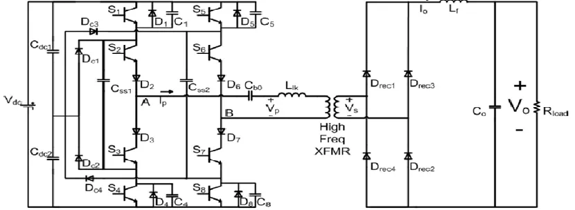
The goal of the design is to produce a dc–dc converter that achieves soft switching for all the main switches, reduces the voltage stresses across each main switch, and controls the voltage on the secondary as per an FB step-down converter. Fig.1 shows the circuit topology and the operational waveforms of the proposed converter. A proposed five level dc-dc converters is presented as shown in fig 1.
Operation of the ZVZCS 5 Level DC-DC Converter Topology: A.
The resistance R-load is the load equivalent resistance and might represent, for example, the inverter interfacing a distribution system. The intermediate voltage stages typically available in a 5L converter (i.e., ±Vdc,0,±Vdc/2) allow a better approximation of a sinusoid thus resulting in a reduction in harmonic levels for the inverter case, but this feature is not applicable to the dc–dc converter here since the output voltage Vout fixed at a constant dc level, is greater than the intermediate levels typical of dc–ac 5L converters. If the intermediate voltages were used, the voltage at the input of the diode-bridge rectifier would be less than Vout and the rectifier would not conduct, so no power would be delivered to the load.
Five-Level Full-Bridge Zero Voltage and Zero Current Switching DC-DC Converter Topology (IJIRST/ Volume 1 / Issue 11 / 001)
The switching scheme, though it does not allow the intermediate voltage levels, does achieve soft switching for all the main devices. Furthermore, the loss of intermediate switching states is consistent with other 3L soft-switched designs. The rectifier diodes Drec1–Drec4 change the transformer voltage so that a positive voltage is applied to the output filter regardless of the polarity of the transformer voltage; thus, the converter’s operation can be defined in terms of half cycles with the voltage and current seen by the output filter Lf –Co being the same for each half cycle. If the converter is in state 1 for duration D × Tsw/2, where D represents the duty cycle and is a fraction between 0 and 1, then the average voltage at the rectifier will be
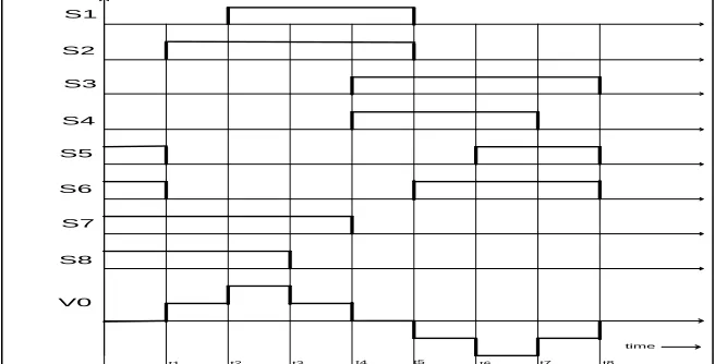
Where n is the turn’s ratio of the transformer. This provides the desired dc voltage conversion and shows that the system operates as a transformer zed buck converter. This Chapter will show how the switching scheme achieves soft switching. Examining Table I and Fig.4.1 reveals that diagonal switches receive the same control signals. The switching scheme can be simplified by controlling the devices in pairs, so that each pair— S1 and S8, S2 and S7, S3 and S6, and S4 and S5—receives the same control signal. It can be further noted that the switching order and duration is identical to phase-shifted PWM for a two level FB, so existing phase-shifted PWM controllers can be used to control the converter. This is an advantage compared to other 3L FB soft-switching topologies which require complex switching control schemes, such as double-phase-shifted control.
Fig. 2: Operational wave forms of the proposed 5 level full bridge converter
Table-1: Switching table
State V
1 - - - - + + + + 0
2 - + - - - - + + ⁄
3 + + - - - - + +
4 + + - - - - + - ⁄
5 + + + + - - - - 0
6 - - + + - + - - ⁄
7 - - + + + + - -
8 - - + - + + - - ⁄
ZVZCS DC-DC Converter Operation Modes: B.
The figure 1.shows the equivalent circuit for the eight operational modes. The following analysis is assumes that the switching period, and the blocking capacitor is large enough to act as a constant voltage source while the current is being reset.
Operational Mode 1: (t0≤t≤t1):
1)
Switches S5,S6 ,S7, and S8 have been ON. Here output voltage is zero and now the rectifying diode does not conduct. Here the capacitors Cdc1 andCdc2 are charged.
Operational Mode 2 :( t1 ≤ t < t2):
2)
Switches S2,S7, and S8 have been ON. As the primary current circulates through Switches S2,S7, Dc1 and Dc4, the blocking capacitor voltage Vcb0p is applied to the transformer and the primary current begins to decrease. As soon as the primary current falls below Ip0, the output current begins to freewheel through the output rectifier diodes, disconnecting the primary side of the circuit from the load and short circuiting the transformer magnetizing inductance. The rectifier diodesDrec1 and Drec2are conducting.
Operation Mode 3: (t2≤t< t3):
3)
Switches S1 and S8 have been ON for a (relatively) long time and Cb0 is charged to –vcb0. Switches S2 and S7 being conducting and (Vdc– vcb0) is applied to the primary of the transformer. As a result the primary current rapidly rises from 0 to the reflected output current. S1 S2 S3 S4 S5 S6 S7 S8 V0
t1 t2 t3 t4 t5 t6 t7 t8
Where IP0 is the peak value of the primary side current going into the transformer, I0 is the Current through Lf, and n is the turn’s ratio of the transformer. The voltage applied to the transformer leakage inductor Llk during this period is Vdc – (- Vcb0) =Vdc+ Vcb0, and the duration of this period is
Since this period is so short, Vcb0 is assumed to be constant throughout the period. The load current is not completely supplied by Vdc during this period, so the excess current freewheels through the secondary rectifier diodes Drec1& Drec2.
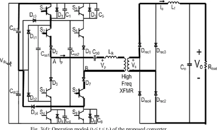
Operation Mode 4: (t3≤t<t4):
4)
Switches S1,S2, and S7 have been ON. The freewheeling mode ends when the primary current reaches Ip0 and diodes Drec3 and Drec4 stop conducting. The output filter is connected in series with the leakage inductance of the transformer through Drec1 and Drec2, and acts to keep the primary current constant at Ip0. The duration of this mode is related to the voltage conversion ratio by the duty cycle parameter D, which is given by
( | ⁄ ) ⁄ ⁄
Operational Mode 5: (t4 ≤ t < t5):
5)
Switches S1,S2, S3,and S4 have been ON. Here output voltage is zero. And now the rectifying diode does not conduct. And primary current reaches to zero. The current does not allow the rectifying side.
Operational Mode 6:(t5 ≤ t <t6 ): 6)
The Switches S6,S3,S4 have been ON. And the diodesDc3,D6 are conducting. Here the rectifying diodes Drec3 and Drec4 conducting. The output filter is connected in series with the leakage inductance of the transformer through Drec3 and Drec4.
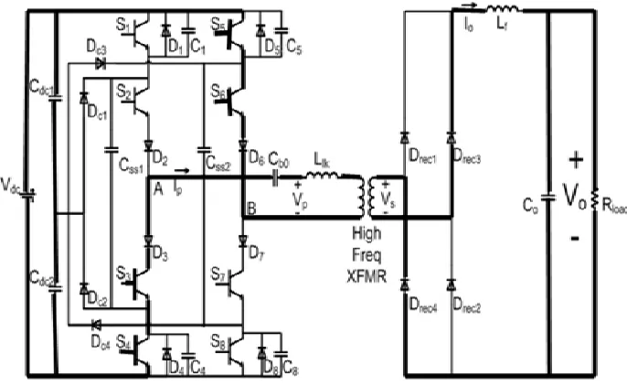
Operational Mode 7:t6 ≤ t <t7):
7)
The Switches S5, S6, S3, S4have been ON. The output voltage is – Vdc and the rectifying diodesDrec3 and Drec4 conduct. Here the primary current flows negative direction. And is charged to . Here the diode D6 also conducts.
Operational Mode 8:(t7 ≤ t <t8):
8)
The Switches S5,S6,S3, have been ON. The output voltage is – Vdc/2. Here the rectifying diodes Drec3 and Drec4 conducting. The output filter is connected in series with the leakage inductance of the transformer through Drec3 and Drec4.
Design Equations: C.
The design of the converter involves determining values for Cdc1, Cdc2, Css1, Css2, C1, C4, C5, C8, The output filter should be large enough to maintain the load current for the entire switching period Tsw, while the Fig. 2 shows that they conduct during mode 3 and its mirror, mode 8. These capacitors must maintain a near-constant voltage during the entire cycle; thus, they should be selected so that they do not experience more than a 5%voltage change during mode 3. Therefore, the capacitor value required for a 5%ripple is
This can be simplified using ,
so that,
The size of the parallel capacitors, Cr, is determined by the minimum requirement to achieve ZVS during turn-OFF, which requires that the parallel capacitors must be large enough to hold the voltage close to zero during the current fall-time of the device , which can be determined from the data sheet. Once this parameter has been determined, Cr can be calculated as
follows
The blocking capacitor will reach its largest value when the converter is transferring maximum rated power and is at . In order to meet the voltage restriction outlined earlier for these conditions, Cb0 should be chosen as
Five-Level Full-Bridge Zero Voltage and Zero Current Switching DC-DC Converter Topology (IJIRST/ Volume 1 / Issue 11 / 001)
Fig. 3: (a)Operation mode1 (t0≤ t < t1) of the proposed converter
Fig. 3(b): Operation mode2 (t1≤ t < t2) of the proposed converter
Fig. 3(d): Operation mode4 (t3≤ t < t4) of the proposed converter
Fig. 3(e): Operation mode5 (t4≤ t < t5) of the proposed converter
Five-Level Full-Bridge Zero Voltage and Zero Current Switching DC-DC Converter Topology (IJIRST/ Volume 1 / Issue 11 / 001)
Fig. 3(g): Operation mode7 (t6≤ t <t7)of the proposed converter
Fig. 3(h): Operation mode8 (t7≤ t <t8) of the proposed converter
Soft-Switching Range: D.
ZVS is accomplished when Ip0 discharges the parallel capacitors across the leading switches during mode 3. The length of mode 3, referred to as the dead time, limits the maximum duty cycle that can be commanded by the controller, which, in turn, limits the maximum voltage that can be achieved on the secondary and the maximum power that can be delivered to the load. Since ZVS, and hence the dead time, occurs twice per half cycle, the maximum duty cycle is
⁄
Once the dead time is fixed, there is a minimum value of the load current under which ZVS no longer occurs since the leading switches will be switched before the parallel capacitors are completely discharged. This minimum load current is given by
ZCS is accomplished when the blocking capacitor voltage drives the primary current to zero before the state change that occurs at Tsw/2. The current begins to be reset at t2 = D × Tsw/2, so the total time available to reset the current is
ZCS will be achieved if the reset period from (6) is less than T reset, max, and using the value for Vcb0pfrom (12)
It can be seen from this equation that achieving ZCS is independent of the load current, though the voltage across Cb0 may become very large if the primary current exceeds the maximum load current used in (10) to calculate the value of the blocking capacitor. There is a limit on the range of duty cycles for which ZCS occurs, givenby
√
√
III.
S
IMULATION RESULTS FOR ZVS FIVE LEVEL DC-
DC CONVERTERIn the above Simulink model, a 100V/25V DC-DC converter has been proposed. In the proposed converter there are totally eight switches. In the positive half cycle diagonal four switches (S1,S2,S7 and S8) will operate and input voltage is applied to primary of the transformer. Similarly in the negative half cycle other diagonal four switches (S3,S4,S5 and S6) will operate and negative voltage is applied to the primary of the transformer. During the switching transitions all the switches operate under soft switching technique. In the proposed model the four outer switches (S1,S4,S5 and S8) operate under ZVS condition and the remaining inner four switches (S2,S3,S6 and S7) operate under ZCS condition.
Five-Level Full-Bridge Zero Voltage and Zero Current Switching DC-DC Converter Topology (IJIRST/ Volume 1 / Issue 11 / 001)
Fig. 5: Operational waveforms of proposed converter
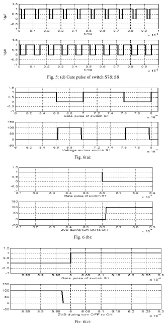
Fig. 5: (a) Gate pulse of switch S1& S2
Fig. 5: (b) Gate pulse of switch S3& S4
Fig. 5: (d) Gate pulse of switch S7& S8
Fig. 6(a):
Fig. 6 (b):
Fig. 6(c):
Fig. 6: simulation (a) switch across voltage (b) ZVS S1, S4,S5, and S8 turn-ON (c) ZVS S1, S4,S5, and S8 turn-OFF
Five-Level Full-Bridge Zero Voltage and Zero Current Switching DC-DC Converter Topology (IJIRST/ Volume 1 / Issue 11 / 001)
voltage across switch S1.condition of switchesS1 and Fig 6(b) shows ZVS turn-ON condition of switch S1. And Fig 6(c) shows ZVS turn-OFF condition of switch S1.And the remaining switches are S4,S5, and S8 to achieve ZVS condition.
Fig. 7(a)
Fig. 7(b):
Fig. 7(c):
Fig. 7: simulation (a) current through switch (b) ZCS S2 turn-ON (c) ZCS S2 turn-OFF
When the pulse is given the voltage across the switch is zero and when pulse is removed the current through the switch is zero Fig 7(a) shows gate pulse of switchS2 and current through switch S2.condition of switches S2 and Fig 7(b) shows ZCS turn-ON condition of switch S2. And Fig 7(c) shows ZCS turn-OFF condition of switchS2. And the remaining switches are S3,S6, and S7 to achieve ZCS condition.
Fig. 5.8 (b):
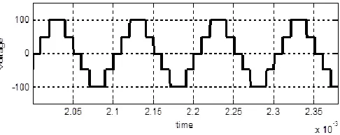
Fig. 8: Simulation (a) Transformer Primary voltage (b) Transformer secondary voltage
With And Without Soft Switching Scheme Tables: E.
With Soft Switching Scheme: 1)
Table- 2: with soft switching scheme5-level DC-DC converter
Load current Input power( ) Output powr ( ) Per switchpwer loss Efficiency (%)
33.98 9054 7124 285 77.3
22.26 7430 5337 176 71.8
17.43 6843 4796 124 70.0
11.85 5460 3527 98 64.59
10.38 5280 3227 92 61.1
Without Soft Switching Scheme: 2)
Table- 3: Without soft switching scheme 5-level DC-DC converter
Load current Input power( ) Output power ( ) Per switch power loss Efficiency (%)
33.98 9067 6736 427 74.3
22.26 6744 4633 275 68.7
17.43 6596 4313 198 65.4
11.85 5213 3279 127 62.2
10.38 5186 3075 110 59.3
Table 2 and Table 3 Shows the efficiency and per switch power loss for different load currents with and without soft switching. For increasing the load current per switch power losses are increases and vice versa. For suppose load current 33.98 Amps, per switch power losses is increased in the five level dc-dc converter without soft switching scheme and efficiency is reduces. If this converter is operating under soft switching scheme for this current the switching losses are decreases and efficiency is increased.
Power Saving Table: 3)
Table- 4.5: level Power saving table
Load current Per switch power loss Power saving (watts) With (watts) Without (watts)
33.98 285 427 142
22.26 176 275 99
17.43 124 198 74
11.85 98 127 29
10.38 92 110 18
Table 4 Shows the power saving and per switch power loss for different load currents with and without soft switching. For example if the load current is 33.98 here power saving is 142 watts.
Filter Elements And THD Table: 4)
Table -5: Filter elements and THD table
Levels L C THD (%)
33.98 9067 6736 427 22.26 6744 4633 275
Five-Level Full-Bridge Zero Voltage and Zero Current Switching DC-DC Converter Topology (IJIRST/ Volume 1 / Issue 11 / 001)
Fig. 9: Efficiency for different load currents
Fig 9 shows Efficiency for various load currents for five level dc-dc converters with and without zero voltage switching scheme. For the same current (33.98A) flow in the converter circuit, the efficiency (74.3%) is less by applying without ZVS and efficiency is more (77.3%) in case of by applying ZVS.
IV.
C
ONCLUSION AND FUTURE SCOPE OF THE WORKConclusion: A.
Resonant converter topologies can be used to increase circuit switching speeds, allowing the cost of circuit magnetic to be reduced, while still keeping switching losses to a minimum. Full wave rather than half wave topologies are generally used, as they generate less EMI. Capacitive switching losses when turning on with a high drain-source voltage means that MOSFETs are more suitable for Zero -Voltage than Zero-Current switches, while its poor turn-off characteristics mean that the IGBT is more suited to Zero-Current topologies.
The dc-dc converter presented here offers significant advantages over traditional designs. The power stage inverter provides efficient dc-dc conversion at very high frequencies, with few small-valued passive components and low device stresses. The multi-stage resonant gate driver developed here provides high-speed, low-loss driving of the inverter. Due to the small values and energy storage of the passive components in both the power stage and gate driver, the transient response can be very fast compared to conventional designs, and the converter is especially well suited to on-off control.
Soft switching scheme is achieved in each and every switch. Voltage stress across each switch was reduced. By increasing the voltage levels the size of the filter elements may also reduced. The switching losses in the proposed converter are reduced. The proposed converter has the advantage of applying full dc bus voltage for the entire operating range. This converter has better switching control scheme compared to traditional three level converters. ZVZCS converters have a wider soft-switching range.
Future Scope: B.
It is possible to implement soft switching scheme for different multilevel inverters. The advantage of soft switching scheme will reduce EMI and switching losses. Therefore the converter efficiency will increase.
R
EFERENCES[1] Joseph Alexander Carr, Student Member, IEEE, Brian Rowden, and Juan Carlos Balda, Senior Member, IEEE,” A Three-Level Full-Bridge Zero-Voltage Zero-Current Switching Converter With a Simplified Switching Scheme,” IEEE TRANSACTIONS ON POWER ELECTRONICS, VOL. 24, NO. 2, FEBRUARY 2009.
[2] C Bor-Ren Lin, and Chia-Hung Chao,"Analysis of Interleaved Three level ZVS converter with series connected transformers," IEEE Trans. on Power Electronics, vol. 28, no. 7, pp. 3088-3099, July 2013.
[3] Ahmad Mousavi, Pritam Das, and Gerry Moschopoulos,"A Comparative study of a new ZCS dc-dc full bridge boost converter with a ZVS active clamp converter ," IEEE Trans. on Power Electronics, vol. 27, no. 3, pp. 1347-1357, Mar 2012.
[4] Joseph Alexander Carr, Brian Rowden, and Juan Carlos Balda,"A Three level Full bridge Zero voltage Zero current switching converter with a simplified switching scheme," IEEE Trans. on Power Electronics, vol. 24, no. 2, pp. 329-338, Feb 2009.
[5] P. dos Santos Garcia Giacomini, J. S. Scholtz, M. Mezaroba, "Step-Up/Step-Down DC–DC ZVS PWM Converter With Active Clamping," IEEE Trans. on Industrial Electronics, vol. 55, no. 10, pp. 3635-3643, Oct 2008.
[6] Bor-Ren Lin, Chien-Lan Huang, Jin-Fa Wan, "Analysis, Design, and Implementation of a Parallel ZVS Converter," IEEE Trans. on Industrial Electronics, vol. 55, no. 4, pp. 1586-1594, April 2008.
[7] Xinke Wu, Junming Zhang, Xin Ye, Zhaoming Qian, "Analysis and Derivations for a Family ZVS Converter Based on a New Active Clamp ZVS Cell," IEEE Trans. on Industrial Electronics, vol. 55, no. 2, pp. 773-781, Feb 2008.