ABSTRACT
PIERSON, BONNIE ELIZABETH. Characterization and Evaluation of a Novel Nanoporous Gold Biosensor Substrate. (Under the direction of Roger J. Narayan.)
Dilute but powerful biological markers, such as hormones in blood stream, are potent but difficult to detect quickly and accurately using current biosensor technologies.
Nanoporous structures offer greatly increased surface area which can be functionalized for use as a biosensor, amplifying throughput and the enhancing the ability to detect small
concentrations. With the option for diverse component materials and conformations, a sensor with prescribed properties could be easily incorporated into devices for clinical diagnosis or research applications. This study evaluates the suitability of a nanoporous gold (NPG) wire for use as a biosensing component as a proof of concept through the detailed characterization of the porosity, structural support, and electrical properties of the wires. The nanoporous gold wires were created using electrochemical etching equipment.
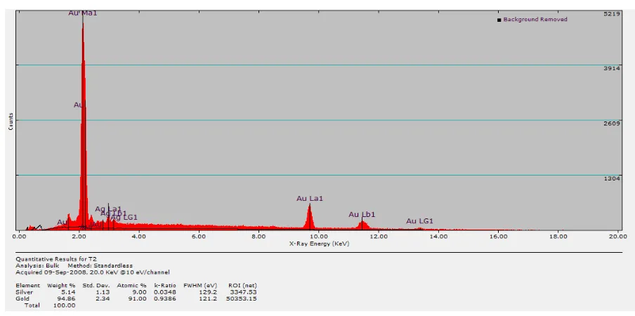
Scanning electron microscopy (SEM) and energy dispersive X-ray spectroscopy (EDS) were used to image and evaluate the pores and effectiveness of the etching procedure. Pores were found to be 9.86 ± 4.92 µm in diameter with a density of 880 pores/µm2 and only 5% silver remained following etching procedures. The storage capacity of the nanoporous wire annealed to a gold support structure at 15.6 mF/cm, was found to be higher than that of unsupported wires at 10.6 mF/cm. Structurally supported NPG wires also demonstrated a lower resistance (4.2Ω compared to 13.4Ω) owing to the capacitance of the nonporous gold support structure at high frequencies.
testing. Some cross-contamination of samples was detected. Most contamination effects were minimal and confined to materials used in the manufacturing process.
Future investigation should include other support structure conformations,
functionalizing samples, and performing biocompatibility testing. NPG wires demonstrate potential for environmental applications and as medical device component, but have not yet been evaluated for direct-contact in vivo applications. The brittleness of the material
Characterization and Evaluation of a Novel Nanoporous Gold Biosensor Substrate.
by
Bonnie Elizabeth Pierson
A thesis submitted to the Graduate Faculty of North Carolina State University
in partial fulfillment of the requirements for the degree of
Master of Science
Biomedical Engineering
Raleigh NC 2009
APPROVED BY:
___________________ Dr. N. Monteiro-Riviere
___________________ Dr. A. Banes
___________________ Dr. R. Narayan
BIOGRAPHY
ACKNOWLEDGEMENTS
This work would not have been possible without the support of the National Science Foundation, whose admirable goals to promote and strengthen scientific research have inspired and encouraged many across disciplines. Further, my gratitude goes out to Dr. Dave Robinson and his research group at Sandia National Laboratories in California for the use of their equipment, careful tutelage in electrochemistry, and supportive environment during my first West coast experience.
TABLE OF CONTENTS
LIST OF FIGURES ...v
LIST OF TABLES ... vii
I. INTRODUCTION ...1
II. BACKGROUND INFORMATION ...5
2.1 NANOPOROUS MATERIALS ...5
2.1.1 POROSITY GUIDELINES ...5
2.1.2 MANUFACTURING NANOPOROUS GOLD ...6
2.1.3 MECHANICAL PROPERTIES ...9
2.1.4 CURRENT APPLICATIONS ...11
2.1.5 SELF-ASSEMBLED MONOLAYERS ...12
2.3 ELECTROCHEMISTRY AND ELECTROCHEMICAL ETCHING ...13
III. EXPERIMENTAL ...17
3.1 OVERVIEW OF METHODS ...17
3.2 OPTIMIZATION OF ETCHING PROCESS...17
3.3 CREATION OF SAMPLES ...21
3.3.1 ELECTROCHEMICAL ETCHING EQUIPMENT ...21
3.3.2 ETCHING PROTOCOL ...22
3.4 ANALYTICAL EQUIPMENT ...23
IV. RESULTS AND DISCUSSION ...25
4.1 POROSITY ...25
4.2 ELECTROCHEMICAL BEHAVIOR ...28
4.3 MECHANICAL AND STRUCTURAL ...34
4.4 CONTAMINATION AND EXTERNAL EFFECTS ...40
V. CONCLUSIONS AND FURTHER WORK ...42
VI. REFERENCES ...47
VII. APPENDIX ...53
A:TESTING INDEX ...54
B:ETCH CONTROLS,MEASUREMENTS,SUMMARIZED ANALYSIS ...55
REGULAR ETCH ...55
LIST OF FIGURES
Figure 1: Basic components of an electrochemical cell. ... 15
Figure 2: Variation of etch parameters. ... 20
Figure 3: Sample with gold wire structural support... 21
Figure 4: Diagram of experimental set up ... 22
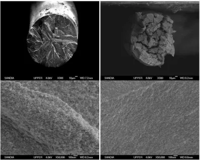
Figure 5: The EDS analysis of the wires indicates a high percentage of gold peaks, with only trace amounts (approximately 5-6%) of silver remaining after etching ... 25
Figure 6: The SEM images of the electrochemically etched wires clearly display the presence of pores on the nanometer scale. (T9) ... 26
Figure 7: Similar Pore Sizes at 50,000x magnification ... 27
Figure 8: CV of nanoporous wire demonstrating transition between capacitor and resistor with increased scan rate (scan rate: 1 V/s, sample T8) ... 29
Figure 9: Movement of charge into the pores with elapsed time at a scan rate of 0.1 V/s. .... 30
Figure 10: Fitting admittance response to circuit model response. ... 31
Figure 11: Admittance averages for wires with and without an external support structure. .. 32
Figure 12: Structural integrity varied with sample handling and conformational support structures. ... 35
Figure 13: Structural reinforcement assisted in maintaining stability with extensive handling of samples. ... 37
LIST OF TABLES
LIST OF TABLES
I. INTRODUCTION
The use of biosensors, devices composed of a biological sensing component coupled with quantitative transduction equipment, has flourished in commercial, clinical, and
research applications in recent years. They allow for fast and accurate testing with reduced time and cost as new development and generations of devices are created. With decreasing size and the advent of multianalyte sensors, less reagent and processing time is required.
Most biosensors are intended for use outside of the body, or mimic in vivo conditions for testing; however there are still biological factors, such as hormones and environmental pollutants that are dilute and difficult to measure effectively with small tissue or fluid samples and requiring low detection thresholds, effectively eliminating the size and reagent advantages of other biosensor applications.
There are several components of a biosensor that can be adapted to address the challenge of low concentration, dilute biomolecules.
1. Surface area. Increased surface area provides the opportunity for improved sensor performance, allowing for the attachment of greater number of biological sensing elements or enhancing alterations in surface chemistry to overcome the low detection threshold.
3. Conformation. The shape of the sensor substrate can aid in maximizing potential surface area, providing mechanical strength in testing situations, and improving handling of equipment.
4. Size. Miniaturization of sensors allows for decreased manufacturing costs as well as lower detection thresholds; however this also changes the signal-to-noise ratio and may require components with specific electrical properties.
5. Cost. Limiting or simplifying the materials and manufacturing methods used can reduce device cost and improve marketability.
With these considerations in mind, a proof-of-concept prototype sensor component was evaluated in this study, with materials and manufacturing methods were selected in such a way to address each of the adjustable device factors described. A gold substrate was
selected because of its well documented biocompatibility and use in electrodes and sensors. It also can provide improved stability in buffering solutions and varied environmental
conditions as compared to other materials such as porous silicon (Bonroy, 2004 and VanNoort, 2000). Creating a nanoporous structure from gold wire was the crux of the prototype design as it provides increased surface area, a lower signal-to-noise ratio
(Szamocki, 2007), double layer capacitance (Wen, 2005), increased yield stress (Hakamada, 2007), a pore size approximate to the diameter of a protein (Sotiropoulou, 2005), and the ability to permit and slow flow through the porous network (Zhang, 2006). Planar
Electrochemical etching of a gold-silver alloy was selected for the creation of a nanoporous gold substrate. This method is well documented and understood, as well as relatively accessible and inexpensive on a larger manufacturing scale. No additional post-processing is required to make the samples suitable for testing.
To address the conformational challenge of a high flow system, a deviation from the traditional two-dimensional planar electrodes was needed. Several researchers have used three dimensional spheres as functionalized microbeads or nanoparticles; however, these must be part of a closed system such as a lab on a chip with a more elaborate transduction procedure, which would be difficult for in vivo applications. A rod or wire shape was selected instead, as it is easily manufactured with the scale and transduction method of a planar gold electrode, but with the mechanical advantages of greater surface area and mechanical strength.
Still, creating an entirely nanoporous substrate makes for an extremely brittle working surface which might fracture during handling or use. To demonstrate the role of structural reinforcement in the performance of the sensor, an alternate conformation of a nanoporous gold wire wrapped and annealed to a spiraling solid gold wire support structure was tested.
Hypothesis:
Nanoporous gold wires formed by electrochemical dealloying of Au-Ag will possess suitable electrical properties and mechanical stability for use as biosensor substrate in medical devices.
Objectives:
• Evaluate electrochemical etching manufacturing method on the basis of porosity control and thoroughness of dealloying.
• Characterize electrical properties of nanoporous gold wires.
• Evaluate changes in electrical properties created by the addition of an external nonporous gold support structure.
II. BACKGROUND INFORMATION
2.1 NANOPOROUS MATERIALS
Recently, increased control over the design and structure of material manufacturing together with the advance of nanoscale features and structures has created renewed interest in the properties of porous materials, particularly on the nanoscale. There are a variety of ways in which nanoporous properties are implemented in sensors. Nanoporous structures may be either selectively or entirely covered or composed of pores. The porous components can be simple or composite materials and may be mounted to the sensor surface or mobile within a device casing. With such an assortment of porous materials to investigate and implement, the specific manufacturing design depends largely upon the specific sensor application.
2.1.1 POROSITY GUIDELINES
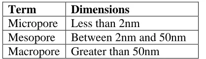
For all porous materials, the dimensions of the pore structures dictate the terminology used in discussing material properties and characterization. Table 1 presents the terms for porosities based on characteristic diameter.
Table 1: IUPAC Guidelines for pore terminology.
Term Dimensions
Micropore Less than 2nm
Mesopore Between 2nm and 50nm Macropore Greater than 50nm
inaccessible pores in the bulk of the material and may cause swelling of polymer substrates, result in fractures or cracks from high temperatures, and may require the destruction of the sample. To account for internal or closed pores, researchers may employ positron
annihilation lifetime spectroscopy (PALS), transmission X-ray scattering (TXS), or transmission neutron scattering (TNS) all of which involve monitoring the effect of or change in various energy beams directed at the sample (Heo, 2006). Other classification methods, such as Atomic force microscopy (AFM) and various types of electron microscopy are frequently used for verification purposes, but may be a primary analytical method in samples with geometries which are particularly challenging to use with more traditional porosity tests.
Evaluating porous structures, there are several measurements that should be
considered in order to obtain a full understanding of the material configuration. In addition to the size of the pores and ligaments, the total surface area, total pore volume, and specific surface area should be determined when possible (Jaroniec, 2002). Further, the transverse porosity of samples should also be considered to ensure the porous matrix consistent throughout the bulk of the material. This information is particularly relevant in instances involving electrodes or materials attached to transduction equipment for calculating the amount of a particular analyte being detected.
2.1.2 MANUFACTURING NANOPOROUS GOLD
the distribution and size of pores. To meet this demand, there is an array of manufacturing techniques used to produce nanoporous structures in many materials by exploiting their self-assembly properties. Polymers and synthetic materials may be manipulated into a porous structure using block copolymer systems, casting, or through the use of self-assembling surfactants (Ding, 2004). However, metallic substrates develop a porous structure chiefly through the removal of another material from an alloy, as occurs in etching or free corrosion, or by depositing the metal onto a substrate, as with spluttering (Zhang, 2006) or vapor deposition (Ding, 2004).
Electrochemical etching and free corrosion involve removing the less noble of two elements in an alloy. The remaining element forms clusters allowing the dissolution/phase separation processes to penetrate further into the substrate until the bulk material is porous. Described and replicated using the Monte Carlo model, the spacing between the clusters of the more noble element of the alloy corresponds to the size of resulting pores (Erlebacher, 2001). Nanoporous metals created through etching have been reported stable with simple post-processing procedures such as a water bath, and are estimated to have a functional shelf life of six months before noting any change in mechanical or electrical properties (Ding, 2004).
in the construction and characterization of electrodes and biosensors using electrochemical or free corrosion etching. It has been suggested that mono-dispersed assemblies with face-centered-cubic formations, in particular, would work to improve signal strength from miniaturized devices (Szamocki, 2007; Zhang 2007). Both gold and silver posses a face centered cubic structure with analogous lattices and solubility characteristics, resulting in plentiful interest in the properties and characterization of etched Au-Ag alloys (Ji, 2003). This corresponding fundamental structure enables the removal of silver during etching and aids in maintaining the polycrystalline face centered cubic structure in the reformation of the gold clusters into a nanoporous material resulting in consistent and desirable mechanical properties (Biener, 2005). Further, nanoporous gold formed from etching in high
concentrations of nitric acid produce extremely clean porous surfaces that can be easily washed and used in sensors and devices with little post-processing (Yin, 2008).
Unique to etched porous metals, the porous product can be post-processed to adjust pore size in the micro- and nano- meter ranges. Annealing the finished product can
drastically change the porosity; increased temperature results in decreased pore size until the metal resumes a solid structure (Ding, 2004). An added benefit of annealing nanoporous gold is the reduction of the defects that can initiate crack nucleation, enhancing the mechanical resilience of a nanoporous piece (Biener, 2005). Other porous manufacturing methods rely heavily on pre-processing on the addition of chemicals to control the pore size and
alloy on porosity, researchers found higher gold concentrations in the Au-Ag alloy resulted in smaller pore sizes for alloys which were deposited as films and then de-alloyed; however, for alloys etched using free corrosion, an increase in the concentration of Au led to a increase in both ligament size and the range of pore sizes present (Ji, 2003).
2.1.3 MECHANICAL PROPERTIES
To fully understand nanoporous gold and establish its suitability for assorted commercial applications, it is important to test and examine its mechanical properties. General observations of NPG quickly establish it as sponge-like with the network of interconnected pores formed from etching; however, the random pore formation is surprisingly consistent throughout the gold structure, allowing for relatively uniform mechanical properties. The extensive porosity also results in a bulk material which on the macroscopic scale is brittle and easily fractured.
On the microscale, nanoporous gold is a much stronger material than its nonporous counterpart. The yield stresses on ligaments in nanoporous gold are higher than solid, polycrystalline gold (Hakamada, 2007). Yield strengths of 145±11 MPa achieved using nano-indentation tests are a full order of magnitude greater than the calculated yield strength of similarly structured nanoporous foams (Biener, 2005).Thus, the nanoporous gold
structures have relatively high yields while maintaining a low density.
ligament breaks (Biener, 2005). Compressive stresses, in particular, have been noted to result in ductile deformation (Biener, 2005); however, the deformation is not widespread
throughout surrounding surface areas, indicating smaller, localized stress fields (Biener, 2005). Still, the structure lends itself to a uniform failure stress, as the failure of one ligament will quickly propagate through the connected network of the porous structure (Biener, 2005). Decreased ligament and pore size therefore results in an increase in yield.
Large lateral grain sizes of several micrometers have been observed in nanoporous gold samples, but were not nucleated by the etching process and demonstrate the material retaining a coherent underlying lattice structure (Ding, 2004). However, these grain
boundaries are susceptible to cracking and fracture even under small stresses. SEM images of nanoporous gold samples have confirmed brittle fractures between the nanocrystalline grain structures similar to those found in original alloyed material (Biener, 2005).
Nanoporous gold leaf, which has been hammered or otherwise mechanically deformed into thin sheets before etching, creates all-gold grain boundaries which are not affected in the etching process and therefore are nonporous (Ding, 2004). This lends significant mechanical stability and support to the structure. Annealing the sample will decrease the pore size and risks of crack propagation (Biener, 2005), but will increase ligament size and reduce the hardness and yield stress of the ligaments (Hakamada, 2007; Biener, 2006).
with a sufficiently small ligament size and appropriate percentage of porosity, nanoporous gold can have a greater mechanical strength than solid, bulk gold (Biener, 2006).
2.1.4 CURRENT APPLICATIONS
Nanoporous materials may be used in a variety of applications. Porous structure can be exploited as a scaffold for growing tissues (Sarka, 2006), coatings for bone implants (Tambasco de Oliveira, 2003), molecular sieves (Vu, 2003), energy storage (Che, 1998), microelectronics (Shelimov, 2000), vessels and substrates for drug delivery (Leoni, 2001), and as electrochemical biosensors (Aravamudhan, 2007). For use in sensors, in particular, the increase in surface area afforded by a porous structure can aid in the generation of a better signal-to-noise ratio (Szamocki, 2007). Research comparing planar porous and planar flat gold electrodes found a significant increase in active surface area with porous substrates (Szamocki, 2007). Furthermore, the scale of the nanopores and nanostructures being investigated are on the same order as the biomolecules sought and employed within biosensor devices, allowing for more fitted interaction between the biomolecules and the sensor (Stylios, 2005). Processing techniques may also be incorporated into device functions and behaviors. For example, just as annealing can be used as a post-processing procedure to reduce pore size, changes in temperature can be used as a controlled drug delivery method in gels and polymers to cause a porous structure to disgorge attached or encapsulated molecules at a regulated rate (Stylios, 2005).
porous material bulk, with large percentages of open volume, is comparable to the extracellular matrix in organisms and consequently can promote a more positive immune response for in vivo devices (Stylios, 2005). As sensors, gold porous materials and structures have also been verified for use with a variety of transduction equipment including
piezoelectric crystals and surface plasmon resonance (Bonroy, 2004). Nanoporous gold biosensors can be used in the manufacture and quality control of food, the development of pharmaceuticals, environmental monitoring, and in clinical applications (Yin, 2008).
2.1.5 SELF-ASSEMBLED MONOLAYERS
Nanoporous gold, as with other substrates used in biosensors, benefits from the addition of a self-assembled monolayer (SAM) of thiols. Many biological sensing molecules and proteins used in biomedical and environmental apparatuses will denature or inactivate upon adsorption onto a non-native surface, such as the device substrate. However, several parameters have been noted to enhance the binding and functionality of these biomolecules including environmental characteristics such as pH and temperature as well as additives and surface treatments such as polyelectrolytes, entrapping matrix substrates, and SAMs
(Sotiropoulou, 2005).
detection (Bonroy, 2004). Alkanethiols, for example, are widely utilized for SAMs in biosensor applications. Long chains are well ordered and stable, acting as barriers to corrosion and provide control over the behavior of a the electrode and signal-to-noise ratio while shorter chains lack the same coherent order resulting in less favorable electrode performance, but simultaneously increasing the double-layer capacitance of the electrode (Cecchet, 2006). As the binding between thiols and sensing proteins are very strong, a SAM will also enhance the strength of protein attachment to the substrate, making devices more robust for a variety of testing environments and handling procedures (Basu, 2004). 2.3 ELECTROCHEMISTRY AND ELECTROCHEMICAL ETCHING
The selective removal of metals from combination materials has a long history, greatly tied to jewelry and artifacts as a surface finishing technique. It provides the appearance of a single metal without requiring a lengthy and difficult purification process and while maintaining the superior mechanical properties of the underlying alloy. Many Incan artifacts, for example, used a copper-gold alloy with a de-alloyed finish to give the appearance of a solid gold piece. Recent investigation into the process of de-alloying did not occur until the late 1960s by Forty and Pickering (Ding, 2004). Depletion gilding, free corrosion, and electrochemical etching are all methods by which a metal may be selectively removed from an alloy (Erlebacher, 2001). Electrochemistry is the methodology employed in this study, and will therefore be of primary focus.
solution, leaving a porous single-component material. Etching can be made part of a circuit such that the chemical reactions can be controlled by the application of voltage and recorded and analyzed using impedance spectroscopy and other electrochemical methods.
For the purposes of this study, a simple and multifunctional three electrode cell was implemented. The change in potential of a controlled, known reaction occurring at one electrode is used as a reference (the reference electrode) against an unknown or unmeasured reaction occurring with a sample of interested (the working electrode). A counter or auxiliary electrode is used to balance the working electrode and prevent current flow to the reference. The reference electrode can be placed in frit to create a half-cell within the cell set-up, creating a more accurate reference point. For electrochemical etching considered in this project, an AuAg alloy functions as the working electrode and relies on an oxidation reaction to remove electrons and cause the silver to move into solution from the alloy.
To characterize electrochemical reactions several techniques have been established, each of which provides insight into the details of the material and interactions occurring in an electrochemical cell. Cyclic voltammetry provides a view of the lag in the system, in terms of current and voltage, to a voltage input. A resistor would result in an inclined line with no lag or storage, whereas a capacitor would be presented as a rectangle. Peaks which occur in the CV recordings represent the anodic and cathodic peaks (Ji, 2003). The result in the electro-etching, or conversely, electro-plating of the working electrode.
current and voltage, which varies based on the capacitive and resistive qualities of the material (Basu, 2004). Admittance is essentially the reciprocal of impedance, reported in Siemens, which can provide greater detail into the capacitive properties of a system. Bot admittance and impedance are complex values, with the real component representing resistive properties and the imaginary part indicating the capacitance. Examining the phasor representation of these properties, the phase angle can provide insight into th
between the resistive and capacitive element of the circuit model.
Figure 1: Basic components of an electrochemical cell.
Data acquired from electrochemical cells is often analyzed in terms of an equivalent circuit model, with capacitance indicating any form of energy storage and resistance
translating into energy release. There are several parameters which will influence
electrochemical data, each affecting the recorded data and theoretical circuit differently. These parameters may then be used to infer and quantify the properties of the material. At high frequencies the resistive and capacitive effects of the bulk cell, primarily the electrolytic
voltage, which varies based on the capacitive and resistive qualities of the Admittance is essentially the reciprocal of impedance, reported in
greater detail into the capacitive properties of a system. Bot admittance and impedance are complex values, with the real component representing resistive properties and the imaginary part indicating the capacitance. Examining the phasor representation of these properties, the phase angle can provide insight into th
between the resistive and capacitive element of the circuit model.
: Basic components of an electrochemical cell.
Data acquired from electrochemical cells is often analyzed in terms of an equivalent t model, with capacitance indicating any form of energy storage and resistance
translating into energy release. There are several parameters which will influence
electrochemical data, each affecting the recorded data and theoretical circuit differently. hese parameters may then be used to infer and quantify the properties of the material. At high frequencies the resistive and capacitive effects of the bulk cell, primarily the electrolytic
voltage, which varies based on the capacitive and resistive qualities of the Admittance is essentially the reciprocal of impedance, reported in
greater detail into the capacitive properties of a system. Both admittance and impedance are complex values, with the real component representing resistive properties and the imaginary part indicating the capacitance. Examining the phasor representation of these properties, the phase angle can provide insight into the relationship
Data acquired from electrochemical cells is often analyzed in terms of an equivalent t model, with capacitance indicating any form of energy storage and resistance
translating into energy release. There are several parameters which will influence
solution, dominates the data recorded (Mirtaher, 2005). Dielectric effects from the coatings would also influence data at this higher range. At low frequencies, the properties and effects of the electrodes are more prominent. A high capacitance at this range often signifies
III. EXPERIMENTAL
This section details the fabrication of samples using electrochemistry and a brief overview of the analytical equipment used to evaluate the samples for suitability in biosensor applications.
3.1OVERVIEW OF METHODS
To create the nanoporous gold wires, a silver-gold alloy wire was electrochemically etched, removing the silver and creating pores in the reformation of gold structure. The parameters of the electrochemical etching process were optimized before production of the final samples. A second set of samples with a spiral gold support structure were produced. The sample sets were then evaluated using electrochemical and analytical spectrographic methods.
3.2OPTIMIZATION OF ETCHING PROCESS
Initially samples were etched using either nitric acid or ammonium nitrate; both are commonly used in electrochemical etches and are well suited to the removal of silver from these silver-gold alloys. A range of concentrations of each solution were used, and the capacitance of the resulting samples was used to identify an optimal concentration. Of solutions between 0.5M and 2M nitric acid, the 1M nitric acid provided the best capacitance and was selected to advance to further SEM imaging and comparison. Similarly, for
ammonium nitrate concentrations between 1M and 15M were used, with 15M creating samples that demonstrated the best electrical properties and highest normalized capacitance. In examining the SEM images of the nanoporous wires created in each solution, the wires etched using ammonium nitrate solution in electrochemical etching demonstrated greater fracturing of samples and slightly larger pore sizes. Given the brittleness of the nanoporous wires, the increased fracturing was of great concern to maintaining structural integrity; therefore, the 1M nitric acid was selected for the samples manufactured for this study.
In a similar fashion, the amount of time the sample spent in the electrochemical cell with an applied voltage was varied from several hours to as few as ten minutes. SEM images of two contrasting times are shown in figure 2, and demonstrate the consistency of pores and effectiveness of etching across a wide time range. Using capacitance to evaluate the
completeness of the etching process, it was found to be roughly the same for samples staying in from thirty minutes to overnight, although exposure times less than twenty minutes were likely to result in an incomplete etch. Using this information, a thirty minute etch was
selected for the samples evaluated in the study; the decreased time allowed for the production of more samples while still maintaining a thorough etch.
To ensure that the temperature of either the 1M nitric acid or the 15M ammonium nitrate would not affect the quality of the porosity produced, both hot and cold etching baths were attempted with both solutions. A cold temperature of 5°C was created and maintained using an ice bath, while and a hot temperature of 35°C was created using a water bath on a hot plate. As glass containers were used for the electrochemical cell, a rubber stopper was used to support the etching solution in the bath to prevent an extreme temperature gradient from forming. Magnetic stirrers were used to facilitate heat transfer and the homogeneity of water temperature surrounding the etching setup. Consistent with our suspicions, the
(Clockwise from top left) (a) Bias of 1.2 V (b) Bias of 1V (c) Etch time of 30 min (d) Overnight etch time.
Figure 2: Variation of etch parameters.
pressures which can result in fracture structural support, half of the silver
smaller solid gold wire wrapped around the particularly fragile segment connecting the etched portion of the wire, which had been submerged in the 1M nitric acid cell, with the unetched top of the wire used for handling samples.
one such structurally supported nanoporous wire.
Figure 3
3.3CREATION OF SAMPLES 3.3.1 ELECTROCHEMICAL
To create the nanoporous gold wires, electrochemical etching was implemented using a cell with a 1M nitric acid solution in a 20mL glass vial with
perchlorate, the silver-gold wire sample to be etched as the
counter electrode submerged in the solution, as illustrated in figure
was connected to potentiostat/galvanostat (Princeton Applied Research, Model 273A) which es which can result in fracture. In order to address this challenge and provide greater
e silver-gold alloy wires to be etched were reinforced with a smaller solid gold wire wrapped around the particularly fragile segment connecting the etched portion of the wire, which had been submerged in the 1M nitric acid cell, with the
ire used for handling samples. Figure 3 shows an SEM of a segment of one such structurally supported nanoporous wire.
3: Sample with gold wire structural support.
AMPLES
LECTROCHEMICAL ETCHING EQUIPMENT
To create the nanoporous gold wires, electrochemical etching was implemented using a cell with a 1M nitric acid solution in a 20mL glass vial with a silver reference electrode
gold wire sample to be etched as the working electrode, and a
counter electrode submerged in the solution, as illustrated in figure 4. The working electrode was connected to potentiostat/galvanostat (Princeton Applied Research, Model 273A) which provide greater gold alloy wires to be etched were reinforced with a smaller solid gold wire wrapped around the particularly fragile segment connecting the etched portion of the wire, which had been submerged in the 1M nitric acid cell, with the
shows an SEM of a segment of
To create the nanoporous gold wires, electrochemical etching was implemented using a cell reference electrode in silver lectrode, and a nickel
was operated through a LabView program written by applied a voltage potential through the potentiostat
out of the silver-gold alloy wire to accumulate on the counter electrode.
Figure
The Labview program allowed for easy control over the potentiostat, including the bias voltage and elapsed time. During the etching process, charge accumulation information was tracked and stored to ensure thoroughness of etching.
3.3.2 ETCHING PROTOCOL
Ten samples were made in each of two conformations: (1) individual, straight gold silver alloy wires with a diameter of 200 µm and (2) a straight gold
diameter) with a supporting structure of solid gold wire (75 µm
was operated through a LabView program written by Dr. Dave Robinson. The program applied a voltage potential through the potentiostat, allowing for the movement of the silver
gold alloy wire to accumulate on the counter electrode.
Figure 4: Diagram of experimental set up.
The Labview program allowed for easy control over the potentiostat, including the elapsed time. During the etching process, charge accumulation information was tracked and stored to ensure thoroughness of etching.
ROTOCOL
Ten samples were made in each of two conformations: (1) individual, straight gold silver alloy wires with a diameter of 200 µm and (2) a straight gold-silver alloy wire (200µm diameter) with a supporting structure of solid gold wire (75 µm diameter) wrapped around it.
Dr. Dave Robinson. The program for the movement of the silver
The Labview program allowed for easy control over the potentiostat, including the elapsed time. During the etching process, charge accumulation information
Alloyed wires were cut 3-4 cm in length and attached to alligator clips. Support structures were created by wrapping 1cm of solid gold wire around the middle of the alloy wire. Supported samples were then annealed to ensure attachment. For all sample sets,
approximately 2cm of the wire was submerged into the electrochemical cell of 1M nitric acid, and run at 1.2V for 30 minutes at room temperature. The wire was then washed in deionized water, and the length of the etched segment measured, before basic
electrochemical tests were performed. 3.4ANALYTICAL EQUIPMENT
IV. RESULTS AND DISCUSSION
4.1POROSITY
The first concern in evaluating a nanoporous biosensor is to establish the size, shape, distribution, and consistency of pores produced by this electrochemical manufacturing method. Porosity is generally evaluated using ellipsometry, which gives an indication of pore size based on the amount of forced gas adsorption; however, the unusual conformation of the sensors in these samples prohibited use of that particular technique. Instead, analytical spectroscopy and electrochemical methods were used to image the pores and examine the properties of the samples.
Figure 5: The EDS analysis of the wires indicates a high percentage of gold peaks, with only trace amounts (approximately 5-6%) of silver remaining after etching.
silver remaining in the samples after etching. An EDS report indicating a 95% etch can be considered a complete etch according to previously published research
Using the resources available through the NCSU Analytical Instrumentation Facility, excellent images of the samples were obtained on both the JEOL 6400F Field Emission Scanning Electron Microscope
These images allow for examination of the dimensions of the nanopores microscopes demonstrate with clarity
the descriptive statistics of pore feature size for several nanoporous samples. compare favorably with previous values established for nanoporous sili pore size of 7.8nm ± 2.4nm and a surface coverage of 10
Figure 6: The SEM images of the electrochemically etched wires clearly display the presence of er remaining in the samples after etching. An EDS report indicating a 95% etch can be
according to previously published research (Biener, 2005). Using the resources available through the NCSU Analytical Instrumentation Facility, excellent images of the samples were obtained on both the JEOL 6400F Field Emission Scanning Electron Microscope and the Hitachi S-3200 Scanning Electron Microscope. These images allow for examination of the dimensions of the nanopores. Both electron
with clarity the meso and micro structures present. the descriptive statistics of pore feature size for several nanoporous samples.
compare favorably with previous values established for nanoporous silica, with an average pore size of 7.8nm ± 2.4nm and a surface coverage of 10-12 percent (Surani, 2005).
: The SEM images of the electrochemically etched wires clearly display the presence of pores on the nanometer scale. (T9)
er remaining in the samples after etching. An EDS report indicating a 95% etch can be (Biener, 2005). Using the resources available through the NCSU Analytical Instrumentation Facility, excellent images of the samples were obtained on both the JEOL 6400F Field Emission
3200 Scanning Electron Microscope. oth electron
Table 2 presents the descriptive statistics of pore feature size for several nanoporous samples. These statistics
ca, with an average (Surani, 2005).
Table 2: Summary of
Average Diameter (nm) Standard Deviation (nm) Pore Density (# pores/um Surface Coverage
Previous studies have noted an increase in ligament and pore size with annealing of gold in post processing (Hakamada, 2007). However, the nanoporous wires in this study which underwent this heating procedure were annealed as part of a pre
process, attaching the solid gold support structure in. SEM images, as in figure demonstrates the comparable pore sizes of etched wires with and without a pre annealing step.
(a) T10 side: Functionalized, no gold support structure
Figure 7: Similar Pore Sizes at 50,000x magnification : Summary of pore statistics from Hitachi SEM images
Average Diameter (nm) 9.86
Standard Deviation (nm) 4.92
Pore Density (# pores/um2) 880.086
Surface Coverage 7.15%
Previous studies have noted an increase in ligament and pore size with annealing of gold in post processing (Hakamada, 2007). However, the nanoporous wires in this study which underwent this heating procedure were annealed as part of a pre-etch preparation process, attaching the solid gold support structure in. SEM images, as in figure
demonstrates the comparable pore sizes of etched wires with and without a pre
T10 side: Functionalized, no gold support structure (b)T13 side: Functionalized with Gold Support Structure
: Similar Pore Sizes at 50,000x magnification. mages.
Previous studies have noted an increase in ligament and pore size with annealing of gold in post processing (Hakamada, 2007). However, the nanoporous wires in this study
etch preparation process, attaching the solid gold support structure in. SEM images, as in figure 7, demonstrates the comparable pore sizes of etched wires with and without a pre-etch
A calculation for the total thickness of entirely porous materials proposed by Szamocki (2007) can be used to approximate the number of pores in a cross section of the wire.
Total Thickness = Number of pore layers + the last half-pore-layer
For the purposes of this study, the total thickness of the wire is known, as well as the relative pore size, and as such an estimation of the number of pore layers in the interconnected network can be estimated.
200µm = 200,000 nm = Number of pore layers * 9.86 nm pore size + ½*9.86 nm pore size Thus, roughly 20,283 pores span the diameter of a cross sectional cut of the porous wire. The number is likely different, simply owing to the fractured and brittle nature of the etched wires and the randomness of pore formation; however it serves as an adequate
estimate providing an indication of scale relative to the macroscopic dimensions of the wire. 4.2ELECTROCHEMICAL BEHAVIOR
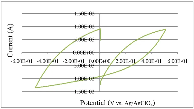
A battery of electrochemical tests were performed to evaluate the electrical properties of the nanoporous gold substrate and to determine the suitability for electrode applications. Cyclic voltammetry performed on the untreated samples demonstrated a transitional behavior from a capacitor to a resistor with increased scanning rates. This is the expected response (Chidsey, 1990) as increased sweep rates will allow less penetration into the interconnect pores and decreased charge storage commonly associated with capacitors. Therefore
illustrates the merging capacitive and resistive properties of a sample, developing a box shape while still maintaining a linearly increasing slope indicative of a resistor.
Figure 8: CV of nanoporous wire demonstrating transition between capacitor and resistor with increased scan rate (scan rate: 1 V/s, sample T8)
The capacitance of the samples can be ascertained from the CV recordings by multiplying the current at the upper intercept by the scan rate. This calculation was
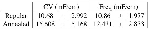
performed for all samples and the resultant values are summarized in table 3. It is clear that there is substantial variation within each sample set, however the length of the wire
characterized can influence the available capacitance, and normalized values are provided in table 5.
Table 3: Average capacitance calculated from cyclic voltammograms of samples with and without an annealed support structure.
Capacitance (mF) Regular (8) 11.69 ± 4.233 Annealed (10) 18.6 ± 9.75
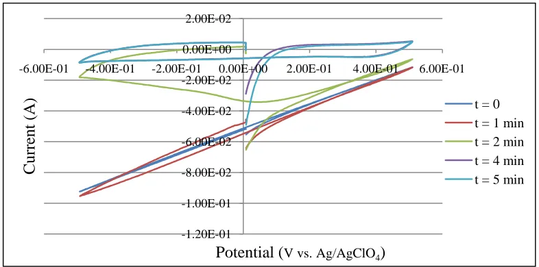
A change in the CV response of samples was also noted for a lower sweep rate held constant over time. As shown in figure 9, the transition of sample behavior from purely
-1.50E-02 -1.00E-02 -5.00E-03 0.00E+00 5.00E-03 1.00E-02 1.50E-02
-6.00E-01 -4.00E-01 -2.00E-01 0.00E+00 2.00E-01 4.00E-01 6.00E-01
C
ur
re
nt
(
A
)
resistive to primarily capacitive is evident. This is likely due to the movement of charge into the porous bulk. After five minutes in solution, the porous wires respond to CV sweeps in a closer approximation to the box shape which would be expected.
To accommodate this movement of charge, approximately four to five minutes were allotted for the samples to soak in the solution of the electrochemical cell before any data was recorded or expected capacitances produced. As such, any data and sweeps recorded within the first few minutes were not included in calculated values, but were used to facilitate and verify the movement of charge into the nanoporous wire structure.
Figure 9: Movement of charge into the pores with elapsed time at a scan rate of 0.1 V/s.
Unfortunately, extensive cyclic voltammetry runs, imputing potential steps into the nanoporous wire and electrochemical cell, will eventually result in a coarsening of the material (Zhang, 2007). Efforts were made to limit the number of runs performed on each sample.
-1.20E-01 -1.00E-01 -8.00E-02 -6.00E-02 -4.00E-02 -2.00E-02 0.00E+00 2.00E-02
-6.00E-01 -4.00E-01 -2.00E-01 0.00E+00 2.00E-01 4.00E-01 6.00E-01
C
ur
re
nt
(
A
)
Potential (V vs. Ag/AgClO4)
A quantitative capacitance was estimated from t
representation of the porous nanowires was used as a model and the resulting equation for admittance was adjusted and fitted to the actual data, providing capacitance and resistance values.
Figure 10: Fitting admittance response to circuit model response.
The model was adjusted to a logarithmic scale and used a least squares method to approximate the fit and parameter values. The frequency responses of two of the regular etch samples were disregarded as they were noted to make incomplete contact with the electrode lead and the data was sufficiently different to warrant exclusion.
A quantitative capacitance was estimated from the admittance plots. A circuit representation of the porous nanowires was used as a model and the resulting equation for admittance was adjusted and fitted to the actual data, providing capacitance and resistance
: Fitting admittance response to circuit model response.
The model was adjusted to a logarithmic scale and used a least squares method to approximate the fit and parameter values. The frequency responses of two of the regular etch
disregarded as they were noted to make incomplete contact with the electrode lead and the data was sufficiently different to warrant exclusion.
he admittance plots. A circuit representation of the porous nanowires was used as a model and the resulting equation for admittance was adjusted and fitted to the actual data, providing capacitance and resistance
: Fitting admittance response to circuit model response.
The model was adjusted to a logarithmic scale and used a least squares method to approximate the fit and parameter values. The frequency responses of two of the regular etch
Figure 11: Admittance averages for wires with and without an external support structure.
As figure 11 illustrates, the admittance response to a range of frequencies provides insight into shifts in material behavior. The structurally supported and annealed wires present an admittance which is shifted to lower frequencies, indicating a slightly higher capacitance (Jagminas, 2007). Both conformations of nanoporous gold wire function as ideal capacitors up to the same high frequency, at which time the resistance of the solution becomes
dominant. Resistance, however, is significantly higher in samples without a nonporous gold support structure. The un-etched gold used to support the annealed samples exhibits
capacitance at higher frequencies than the porous gold, resulting in lower resistance at higher frequencies.
Table 4: Fitted estimates from the admittance model.
Capacitance (mF) Resistance (Ω) Slope Regular (8) 11.75 ± 2.67 13.41 ± 6.61 17.55 ± 1.22 Annealed (10) 14.45 ± 6.74 4.22 ± 2.57 19.1 ± 0.25
0 0.5 1 1.5 2 2.5 3 3.5
0.001 0.1 10 1000 100000
A
dm
it
ta
nc
e
(dB
)
Frequency (Hz) log scale
The slope of the frequency response is very similar across sample sets, demonstrating a good consistency of behavior. However, some of the variation in capacitance is a function of the length of the etched wire undergoing characterization. To offset the influence of length, samples were measured following characterization and a normalized capacitance calculated for both frequency response values and cyclic voltammetry readings. As shown in table 5, the variance between samples is much more consistent and constrained using
normalized values, and the admittance values of the frequency response appear are a superior metric of capacitive properties, likely due to the incorporation of a least squares fitting procedure into the model matching procedure.
Table 5: Average normalized capacitance.
CV (mF/cm) Freq (mF/cm) Regular 10.68 ± 2.992 10.86 ± 1.977 Annealed 15.608 ± 5.168 12.431 ± 2.833
structural component provides increased capacitance, particularly at high frequencies, where the resistance of the electrolyte solution is reduced.
While the nanoporous structure of the gold wires did not produce the high
capacitance values of a double layer capacitance supercapacitor, it demonstrates some of the underlying principles leading to the creation of one. Increased pore density increases capacitance, but only at low frequencies and through pores with a certain size range. High capacitance components can be valuable in high voltage devices.
4.3MECHANICAL AND STRUCTURAL
With ample analytic images of the samples, observations of the structural soundness of the wire conformation together with mechanical testing of nanoporous gold materials found in literature can be used to evaluate the suitability of the sensor for use in vivo or in environmental applications.
As discussed in the introduction to nanoporous materials, nanoporous gold acts an interconnected, sponge-like network of pores with generally uniform properties. Porosity decreases the density of the wires, but studies have shown the yield strength to be higher than expected using scaling laws (Biener, 2005). Using samples created through similar
electrochemical etching of alloyed gold-silver material, an average yield strength of 145±11 MPa and a modulus of 11.1 ± 0.9 GPa were established using nano-indentation tests (Biener, 2005).
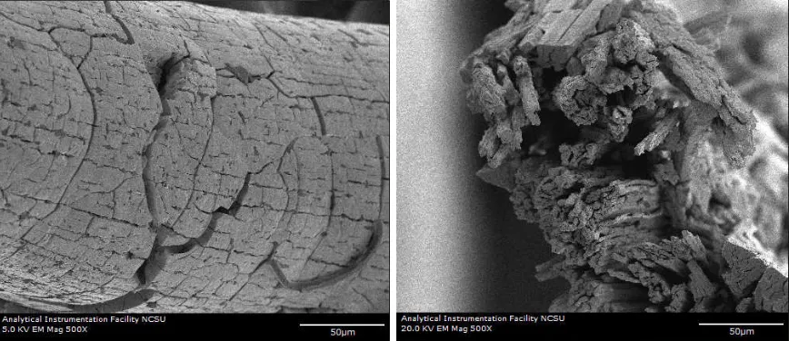
undergo mechanical failure. Figure 12 shows both external fractures as well as internal “stringing” caused by a combination of gold reformation after de-alloying and propagated fractures. However the macroscopic wire functioning as a bundle of nanoscale rods and wires can retain a high yield stress (Hakamada, 2007)
Although the rod conformation provides increased exposed surface area for
functionalization, such shapes accumulate charge at the sharp tips of the end and can throw off electrode readings. The increased fracture of brittle nanoporous wires further increases the current density at the fractured ends, as can be seen in figures 12b and 13a, which is beneficial in applications which require increased capacitance, but can offset any established calibration curves.
(a) Lateral view of a structurally supported wire which retained greater the uniformity of the rod
conformation (sample T20). (b) Cross-sectional view of fracturing caused by cutting samples for characterization (sample T9).
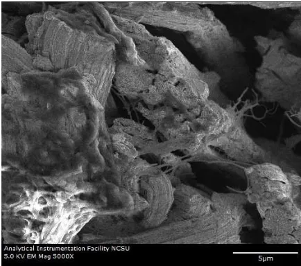
Characterization and testing of the samples required a great deal of mechanical stressors, including transport, handling, and purposeful fracture of samples into smaller samples components for destructive or outsourced tests. In particular, working with samples on such a small scale necessitates handling them with specialized tools, particularly tweezers, to transport while preventing contamination. However, these tools often apply high force on a small and concentrated surface area, usually resulting in fractures. Some samples, such as the one in figure 13a, were moved repeatedly to prepare for imaging and required the application of additional force to ensure effective electrical contact with the carbon tape of the sample holder. Excessive handling, in this instance, resulted in complete destruction of the original rod conformation. This had the advantage of providing added insight into the formation of the nanoporous bulk, illustrating the component fibers formed from the gold clusters during etching. Still, it exemplifies the inability to use nanoporous gold wires in high pressure applications, or as a component in a device or sensor which will require extensive handling during use or manufacture without an inadequate support structure.
Despite addition of a solid gold support structure, annealed to the wire before etching, the brittleness of the nanoporous segments resulted in some splintering with extensive
manipulation and handling; however it was much improved from the unsupported
damage to the sensor within. Electroanalytical testing also found the gold support structure to improve overall capacitance, particularly at high frequencies, thereby improving sensor performance.
(a) Excess handling results in wide
provides some improvement in preventing material failure (sample T20).
Figure 13: Structural reinforcement assisted in maintaining stability with extensive handling of
SEM images of the samples, as in figure
nanocrystalline grain structures similar to that found in original alloyed material. Researchers have estimated the crystallite size of gold to be around 30nm
keeping with the size of the “strings” or rods of which the macroscopic nanoporous wires appear to composed. This grouping may also be caused by the clusters of accumulated gold formed during the removal of silver in the de
damage to the sensor within. Electroanalytical testing also found the gold support structure to all capacitance, particularly at high frequencies, thereby improving sensor
Excess handling results in wide-range fracture (sample T2) (b) A support structure provides some improvement in preventing material failure (sample T20).
: Structural reinforcement assisted in maintaining stability with extensive handling of samples.
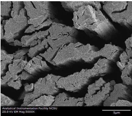
SEM images of the samples, as in figure 14, revealed brittle fractures between the nanocrystalline grain structures similar to that found in original alloyed material. Researchers
crystallite size of gold to be around 30nm (Biener, 2005), which is in “strings” or rods of which the macroscopic nanoporous wires appear to composed. This grouping may also be caused by the clusters of accumulated gold formed during the removal of silver in the de-alloying process.
damage to the sensor within. Electroanalytical testing also found the gold support structure to all capacitance, particularly at high frequencies, thereby improving sensor
range fracture (sample T2) (b) A support structure provides some improvement in preventing material failure (sample T20).
: Structural reinforcement assisted in maintaining stability with extensive handling of
, revealed brittle fractures between the nanocrystalline grain structures similar to that found in original alloyed material. Researchers
Figure 14: Fractures along grain boundaries (sample T7).
While nanoporous gold with appropriately sized ligaments and small pore sizes will experience increased mechanical strength and hardness (Hakamada, 2007), extremely small feature sizes such as those less than 10nm in diameter will cause a reduction in the strength of the bulk porous material (Biener, 2006). The pore sizes of the nanoporous gold wires created in this study hovered around the 10nm mark (see table 2). The degree of porosity also plays a role in the mechanical strength nanoporous gold of a similar pore size to the samples manufactured in this study, but at 75% porosity has been shown to be stronger than solid, bulk gold samples (Biener, 2006). Due to the wire conformation, ellipsometery was not possible to determine the total volume or percent porosity of the samples. With
electrochemical etching of a 50%wt Au-Ag alloy, for a thorough etch as verified by EDS the samples would be around 50% porosity.
This can be advantageous in reducing pore size and thereby increasing resistance, but would also be likely to negatively impact any attached surface chemistry. It is possible that some of the internal propagating fractures, seen in the cross-sectional views and fraying of some samples, may be caused by this extensive coarsening.
Most research into the mechanical stability and failure of nanoporous materials has been on relatively static rather than dynamic loading (Surani, 2005). While no fluid flow studies have been performed with alternate conformations of nanoporous gold, such as the rod morphology of nanoporous wires, several have been conducted on nanoporous
Regardless of the factors causing the considerable fracturing of some of the samples, it remains clear that the nonporous gold structural support provides improved mechanical behavior as well as superior electrochemical performance with improved capacitive properties.
4.4CONTAMINATION AND EXTERNAL EFFECTS
In evaluating the effectiveness of any device or component it is critical to examine the samples for any signs of contamination from manufacturing, handling, or testing and to note any adverse impacts that occur as a result of exposure to the environment. Attempts were made to characterize and quantify cross-contamination as well as to identify sources.
Small deposits of silicon, sodium, aluminum oxide, and potassium chloride were identified using EDS, as pictured in figure 15. These elements were likely contributed by the solutions and electrodes used to manufacture and electrochemically test the samples. Such small remnants were not widely represented on the samples and tended to aggregate in the same small regions, further implicating handling and manufacturing processes as the causes. While these minute contaminations are unlikely to have a significant effect on the
capacitance or sensor behavior in relation transduction, such contamination should be closely monitored and would not be permitted for medical applications. Contaminants from
(a) Silicon, Sodium, and Oxygen (b)
Figure 15: Some samples also displayed remnants of the electro
(a) Silicon, Sodium, and Oxygen (b) Aluminum Oxide (c) Potassium Chloride
: Some samples also displayed remnants of the electro-chemical solutions and tools used in processing.
Potassium Chloride
V. CONCLUSIONS AND FURTHER WORK
The study objectives may be addressed with the data accumulated and used to evaluate the initial hypothesis.
• Evaluate electrochemical etching manufacturing method on the basis of porosity
control and thoroughness of dealloying.
Evaluation of the etching procedure would suggest it to be an acceptable and simple procedure for the creation of nanoporous gold structures on a large scale. EDS evaluation of the cross-section of samples confirmed only 5% of the nanoporous sample was silver. Less silver is present on the external surface area, as the etching process moves inward through the sample. This is preferred for biosensing applications as completely gold surface will provide an optimum binding surface for biomolecules and would provide improved biocompatibility with tissue or fluid samples.
The porosity of the samples was critical component to the sensor function and desired properties. The pore size achieved through electrochemical etching was appropriate for application as a biosensor, at around 10µm in diameter, but the variance in the sizes of pores was too large for this to be considered an ideal manufacturing method. Further adjustments to the procedure are needed to decrease variance while maintaining this preferred range of sizes. The density of pores present on the surface was sufficient at 880 pores/µm2. However, again, the variance in pore sizes present reduces the uniformity of coverage and the
percentages throughout the wires increase the fragility of samples, therefore a balance between pore coverage and structural strength should be negotiated.
Some contamination from manufacturing equipment and supplies was noted. All contaminating elements were either present in the electrochemical cell and being used directly in the manufacturing process, or were being used in conjunction with other samples undergoing electrochemical characterization at the same time. Establishing a batch testing procedure would aid in eliminating contamination from shared equipment.
• Characterize electrical properties of nanoporous gold wires.
Through electrochemical evaluation, the capacitance of the samples was examined in detail. Some increased charging from double-layer capacitance was noted, though the mechanical fraying of wires which occurred with handling likely reduced this effect. While the normalized capacitance of the nanoporous gold wires is less than could be achieved with more complicated porous sensors, with less materials and processes involved in
manufacturing the wires would have lower production costs and could be more easily
• Evaluate changes in electrical properties created by the addition of an external
nonporous gold support structure.
The presence of a support structure, in addition to mechanical stability, provided increased capacitance over a larger range of frequencies. It would be possible, therefore, to attach transduction equipment to the gold support structure for improved signal while retaining the capacitive and sensor substrate benefits of the porous gold medium. The structurally supported samples demonstrated higher capacitive values, but greater variance between electrochemical analytic tests and between samples. The improved capacitance at high frequencies does decrease the impact of the resistance of the electrolyte solution in the cell. This significantly reduces the overall resistance to 4.2Ω, compared to an unsupported nanoporous gold wire average of 13.4Ω. These resistive properties can have distinct advantages in select medical applications.
• Evaluate changes in mechanical performance with the addition of an external
nonporous gold support structure to the nanoporous wires.
The initial hypothesis proposed that nanoporous gold wires formed by electrochemical dealloying of Au-Ag will possess suitable electrical properties and
mechanical stability for use as biosensor substrate in medical devices. On the basis of the
data accumulated, it is apparent that the hypothesis is not supported in its entirety. While electrochemical etching is an affordable manufacturing technique, it does not provide consistent or well controlled porosity within appropriate bounds. The electrical properties of the wire are suitable, and even improved with the presence of an external support structure; however, the mechanical stability of the substrate is not satisfactory for biosensor
applications.
Figure 16: Biological residue, proteins on an untreated nanoporous wire. (Sample T7)
VI. REFERENCES
Aravamudhan, A., Ramgir, N.S., and S. Bhansali. 2007. Electrochemical biosensor for targeted detection in blood using aligned Au nanowires. Sensors and Actuators B: Chemical. 127(1): 29-35.
Balasubramanian, S., Revzin, A., and A. Simonian. 2006. Electrochemcial desorption of proteins from gold electrode surface. Electroanalysis, 18 (19-20): 1885-1892.
Baselt, D.R., Lee, G.U., Natesan, M., Metzger, S.W., Sheehan, P.E., and R.J. Colton. 1998. A biosensor based on magnetoresistance technology. Biosens.s and Bioelec. 13(7-8): 731-739.
Basu, M., Seggerson, S., Henshaw, J., Jiang, J., del A Cordona, R., Lefave, C., Boyle, P.J., Miller, A., Pugia, M., and S. Basu. 2004. Nano-biosensor development for bacterial detection during human kidney infection: Use of glycoconjugate-specific antibody-bound gold
NanoWire arrays (GNWA). Glycoconjugate J. 21(8-9): 487–496.
Biener, J., Hodge, A.M., and A.V. Hamza. 2005. Microscopic failure behavior of nanoporous gold. Appl. Phys. Lett. 87(12).
Biener, J., Hodge, A.M., Hamza, A.V., Hsiung, L.M., and J.H. Satcher. 2005. Nanoporous Au: A high yield strength material. J. Appl. Phys. 97(2).
Biener, J., Hodge, A.M., Hayes, J.R., Volkert, C.A., Zepeda-Ruiz, L.A., Hamza, A.V., and F.F. Abraham. 2006. Size effects on the mechanical behavior of nanoporous Au. Nano Lett. 6(10): 2379-2382.
Blonder, R., Katz, E., Cohen, Y. Itzhak, N., Riklin, A., and I. Willner. 1996. Application of redox enzymes for probing the antigen-antibody association at monolayer interfaces: development of amperometric immunosenor electrodes. Anal. Chem. 68(18): 3151-57. Bonroy, K., Friedt, J-M., Frederix, F., Laueyn, W., Langerock, S., Campitelli, A., Sara, M., Gorghs, G., Goddeeris, B., and P. Declerck. 2004. Realization and characterization of porous gold for increased protein coverage on acoustic sensors. Anal. Chem. 76: 2499-4306.
Cecchet, F., Marcaccio, M., Margotti, M., Paolucci, F., Rapino, S., and P. Rudolf. 2006. Redox mediation at 11-Mercaptoundecanoic acid self-assembled monolayers on gold. J. Phys. Chem. 110: 2241-2248.
Chidsey, C., and D. Loiacono. 1990. Chemical functionality in self-assembled monolayers: structural and electrochemical properties. Langmuir 6: 682-691.
Ding, Y., Kim, Y., and J. Erlebacher. 2004. Nanoporous gold leaf: "ancient technology." Adv. Mat. 16(21): 1897-1900.
Doi, N., and H. Yanagawa. 1999. Design of generic biosensors based on green fluorescent proteins with allosteric sites by directed evolution. FEBS Lett. 453(3): 305-307.
Edelstein, R., Tamanaha, C., Sheehan, P., Miller, M., Baselt, D.R., Whitman, L.J., and R.J. Colton. 2000. The BARC biosensor applied to the detection of biological warfare agents. Biosens. and Bioelec.14(10-11), 805-813.
Erlebacher, J., Aziz, M.J., Karma, A., Dimitrov, N., and K. Sieradzki. 2001. Evolution of nanoporosity in dealloying. Nature 410(6827): 450-453.
Evans-Nguyen, K., Tao, S., Zhu, H., and R. Cotter. 2008. Protein arrays on patterned porous gold substrates interrogated with mass spectroscopy: Detection of peptides in plasma. Anal. Chem. 80: 1448-1458.
Fernandes, P. B. 1998. Technological advances in high-throughput screening. Current Opinion in Chemical Biology 2(5): 597-603.
Fu, J., Park, B. Siragusa, G., Jones, L., Tripp, R., Zhao, Y. and Y. Cho. 2008. An Au/SI hetero-nanorod-based biosensor for Salmonella detection. Nanotech. 19(15): 155502. Gee, S., Hong, Y., Erickson, D., Sur, J., and M. Park. 2003. Synthesis and aging effect of spherical magnetite (FeO) nanoparticles for biosensor applications. J. of App. Phys. 93(10): 7560-7563.
Graham, D., Ferreira, H., and P. Freitas. 2004. Magnetoresistive-based biosensors and biochips. Trends in Biotech. 22(9): 455-462.
Hakamada, M. and Mabuchi, M. (2007). Mechanical strength of nanoporous gold fabricated by dealloying. Scripta Materialia, 56, 1003-1006.
Han, M., Gao, X. Su, J.Z., and S. Nie. 2001. Quantum-dot-tagged microbeads for multiplexed optical coding of biomolecules. Nature Biotechnology 19: 631-635.
Heo, K., Yoon, J., Jin, K., and M. Ree. 2006. Characterisation of pore structures in
nanoporous materials for advanced biotechnology. IEE Proc.-Nanobiotechno,153(4): 121-128.
Ivnitski, D., Sitdikov, R., and N. Ivnitski. 2003. Non-invasive electrochemical hand-held biosensor as diagnostic indicator of dental diseases. Electrochem. Comm. 5(3): 225-229. Jagminas, A., Kuzmarskytė, J., Valinčius, G., Malferrari, L. and A. Malinauskas. 2007. Modification of alumina matrices through chemical etching and electroless deposition of nano-Au array for amperometric sensing. Nanoscale Res. Lett. 2: 130-134.
Jaroniec, M. 2002. Characterization of Nanoporous Materials. In Access in Nanoporous Materials, 255-272. NY: Plenum Press.
Ji, C. and P.C. Searson. 2003. Synthesis and Characterization of Nanoporous Gold Nanowires. J. Phys. Chem. B 107: 4494-4499.
Leoni, L. and T.A. Desai. 2001. Nanoporous biocapsules for the encapsulation of insulinoma cells: Biotransport and biocompatibility considerations. IEEE Trans. Biomed. Eng. 48: 11. Macdonald, J.R. 1992. Impedance Spectroscopy. Ann of Biomed Eng. 20: 289-305.
Markgren, P., Hamalainen, M., and U. Danielson. 2000. Kinetic analysis of the interaction between HIV-1 protease and inhibitors using optical biosensor technology. Ana. Biochem. 279(1): 71-78.
Mattigod, S., Parker, K. and G. Fryxell. 2006. Correlation of heavy metal binding capacity of thiol-SAMMS using the Misono softness parameter. Inorganic Chem. Comm. 9: 96-98. Mirtaher, P., Grimnes, S. and O.G. Martinsen. 2005. Electrode polarization impedance in weak NaCl aqueous solutions. IEEE Trans. on Biomed. Eng. 52(12): 2093-2099.
Mishra, A., Bansal, C. and H. Hahn. 2008. Surface charge induced variation in the electrical conductivity of nanoporous gold. J. of App. Physics 103: 094308
Moeller, K.E., Lee, K. and J.C. Kissack. 2008. Urine Drug Screening: Practical Guide for Clinicians. Mayo Clinic Proceed. 83(1): 66-76.