Available online:
https://edupediapublications.org/journals/index.php/IJR/
P a g e | 733Design and Implementation of Double Gate 8T SRAM Cell Using
MTCMOS
Mohammed Imad Uddin & Nagalakshmi E.V
1PG Scholar, Dept of ECE, M.V.S.R Engineering College, Hyderabad, India.
2Assistant Professor, Dept of ECE, M.V.S.R Engineering College, Hyderabad, India.
Abstract: This paper concentrate on the dependability investigation at various draw up proportions and power dissemination of a novel low power 8T MTCMOS SRAM cell. In MTCMOS Technology the SRAM cell contains low VT (LVT) transistors and two high VT (HVT) sleep transistors for rationale usage. The power utilization duringwrite and read method of operation is less and during standby mode leakage power is insignificant in SRAM cell on account of high Vth sleep transistors. To decrease the swing voltage at the yield hubs of the bitline and bitlinebar in view of the two Additional voltage sources are utilized, one is associated with the draw up transistor as sleep and another is associated as sleepbar to pull down transistor. Both these voltages are complimentary to each other. The diminishment in swing voltage causes the lessening in unique power dispersal, low leakage power streams in MTCMOS innovation and the re-enactment consequences of proposed 8T Double gate SRAM cell utilizing MTCMOS cell have been resolved and contrasted with 8T Double gate SRAM cell and the recreation have been done in 45nm CMOS Technology utilizing Tanner EDA Tool.
Keywords: DG (Double gate), MTCMOS (Multi threshold CMOS), Low power, Sleep Transistor, SRAM.
I. Introduction
The SRAM cell design having low power and high stability is required as the demand of the portable electronic market constantly for less power- hungry architectures [1]. Here the same technique is introduced such as scaling the supply voltage using MTCMOS process. The SRAM is to ensure the reasonable noise margin which is normally measured by the static noise margin. According to this design degrade when the threshold voltage variation increases and are also linearly depend on the reduction of the supply voltage. So result is difficult to maintain
the cell stability and technology enters less than 100nm regime [2].
The 8T double gate SRAM cell is design to improve the stability and power dissipation. This Design having separated read and write operations. The static power dissipation and dynamic power dissipation in SRAM cell during write/read operation is minimized. Here the common method is used to improve the read and write operation which is boosted by MTCMOS technique. MTCMOS technology provides low leakage and high performance operation by utilizing high speed, low threshold voltage transistor during active mode and low leakage, high threshold voltage transistor during sleep mode. This technology is also called as power gating. During switching activities two voltage sources are used at the output nodes to reduce the swing voltage resulting in reduction of dynamic power dissipation.
II. Multi Threshold Complementary
Metal
Oxide
Semiconductor
(MTCMOs)
Multi-threshold CMOS (MTCMOS) is a variety of CMOS chip innovation which has transistors with numerous limit voltages (Vth) so as to
advance postpone or power [3]. The Vth of a
MOSFET is the gate voltage where a reversal layer shapes at the interface between the protecting layer (oxide) and the substrate (body) of the transistor. Low Vth gadgets switch quicker,
Available online:
https://edupediapublications.org/journals/index.php/IJR/
P a g e | 734staticleakage power control. High Vth gadgets are
utilized on non-basic ways to decrease static leakage power control immediately punishment. Ordinary high Vth gadgets lessen static leakage
power by 10 times contrasted and low Vth
devices.
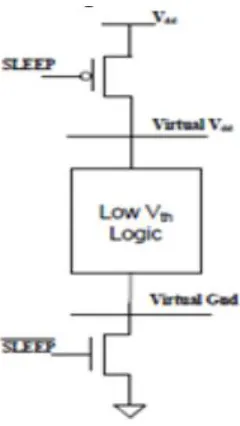
Figure 1: Basic MTCMOS.
Multi-threshold CMOS (MTCMOS) is the most
generally utilized leakage power control
concealment method in best in class incorporated circuits [4]. In a MTCMOS circuit, high limit voltage (high-| Vth|) sleep transistors (header or
potentially footer) are utilized to remove the power supply as well as the ground associations with a sit still low threshold voltage (low-| Vth|)
circuit hinder as represented in Fig.1. In a power-gated MTCMOS circuit, a high-| Vth| header is
appended between the chip control circulation organize (specifically associated with the power supply) and a virtual electrical cable (associated with the low limit voltage circuit hinder). On the other hand, in a ground-gated MTCMOS circuit, a high-| Vth| footer is embedded between the chip
ground dissemination organize and a virtual ground line (associated with the low limit voltage circuit hinder). In a power and
ground-gated MTCMOS circuit, both a high-| Vth| header
and high-| Vth| footer are used to square access to
the chip power and ground circulation systems, as delineated.
A) ACTIVE Mode
In ACTIVE mode, the header and footer sleep transistors are initiated, as appeared in Fig.1. The virtual electrical cable in the power-gated MTCMOS circuit is charged to VDD [3][4]. On the other hand, the virtual ground line in the ground-gated MTCMOS circuit is released to 0V. The powerful supply voltage experienced by the low-| Vth| circuit piece is VDD. The
MTCMOS circuit in this manner keeps up superior like an absolutely low-| Vth| circuit.
B) SLEEP Mode
In SLEEP mode, the header and footer sleep transistors are sliced off to bring down the subthresholdleakage power streams [3][4]. The virtual electrical cable in the power-gated MTCMOS circuit is regularly released to an enduring state voltage level that is near 0V by the leakage power streams of the low-| Vth|
circuits. Then again, the virtual ground line in the ground-gated MTCMOS circuit is commonly charged to a consistent state voltage level near VDD by the leakage power streams of the low-| Vth| circuits. In the power and ground-gated
MTCMOS circuit, both the virtual electrical cable and virtual ground line are kept up at voltage levels amongst VDD and 0V in SLEEP mode. The leakage power streams of a sit out of gear MTCMOS circuit are controlled by the cut-off high-| Vth| sleep transistors. The leakage
power control utilization of a MTCMOS circuit is subsequently essentially lessened in SLEEP mode when contrasted with a simply low-| Vth|
Available online:
https://edupediapublications.org/journals/index.php/IJR/
P a g e | 735III. Circuit Design of 8T SRAM and 8T
SRAM with MTCMOS
On chip cache represents a large portion of the chip and it is expected to increase in future in both portable devices and high performance processors. To achieve higher reliability and longer battery life for portable applications, low power cache is a necessity. As CMOS technologies continue to scale down to deep sub-micrometer levels, devices are becoming more sensitive to noise sources. Systems-on-a-Chip (SoCs) and other integrated circuits today are writed of nanoscale devices that are crammed in small areas [5].
Two different SRAM cells are described in this section, assuming a 45-nm technology. Tanner EDA Tool is used to characterize the SRAM cells.
A) 8T Double gate SRAM cell
Eight-transistor (8T) SRAM cell with Double gate FETs is shown in Fig.2 is designed [6][7]. Two additional p-type transistors are connected in parallel with the n-type bitline access transistors. The n-type bitline access transistors are controlled by a write wordline (WL) signal. Meanwhile, the p-type bitline access transistors are controlled by a read/WL (RWL) signal. The WL is shared by a word and the RWL is shared by a row of cells in a memory array.
Figure 2: Schematic of 8T SRAM
Preceding a write operation with 8T double gate SRAM, approaching information and correlative information are exchanged to the bitlines. One of the bitlines is released to 0 V. Like, the WL and RWL flag change to Vdd and Vgnd, separately, to
start a write operation. The new information and corresponding information are constrained into the SRAM cell through the writebitline transmission gate as shown in fig 9.
Like the customary 6T memory circuits, the read operation with the proposed SRAM cell is differential. RWL and WL are kept up at Vdd and
Vgnd, individually, in an unaccessed (sit still) SRAM cells. The bitlines are pre-charged to Vdd
preceding a read operation []. RWL changes to Vgnd to start the read operation. The read bitline get to transistors (P3 and P4) are, in this manner, turned-ON. Given that a 0 is put away on Node-1, BL-1 is released through the transistor stack that is shaped by P3 and N1. Contingent upon the voltage level of bitlines, the put away information are distinguished by a sense amplifier that is connected to BL-1 and BL-2 as shown in fig 8.
The standby method of operation of 8T SRAM cell is appeared in fig 10.
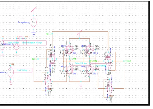
B) 8T Double gate SRAM cell using MTCMOS
Another 8T-SRAM cell using MTCMOS with eight tied-gate FETs is proposed in this work for
accomplishing improved read information
steadiness, more grounded write capacity, and
speedier information exchange without
Available online:
https://edupediapublications.org/journals/index.php/IJR/
P a g e | 736and another n-type is taken as sleepbar in the pull-down network. The pull-up transistors acts as high Vth and pull-down transistor acts as low
Vth. The whole circuit is operated depending
upon these two transistors. The WL is shared by a word and the RWL is shared by a line of cells in a memory array.
The read and write operation of the proposed 8T double gate SRAM cell using MTCMOS is similar to that of 8T double gate SRAM cell.
Figure 3: Schematic of 8T Double gate SRAM cell using MTCMOS
Going before a write operation with proposed SRAM, the sleep transistors are enabled and the pull-up sleep transistor is acts as Vdd, moving
toward data and correlative data are traded to the bitlines. One of the bitlines is discharged to 0 V. Like, the WL and RWL signal change to Vdd and
Vgnd, independently, to begin a create operation. The new data and relating data are compelled into the SRAM cell through the form bitline transmission gates. The voltage margin and data trade speed in the midst of form operations are, along these lines, updated with the proposed SRAM cell as differentiated and 8T SRAM cells as showed up in fig 12.
Like the conventional 8T memory circuits, the read operation with the proposed SRAM cell is differential. RWL and WL are kept up at Vdd and
Vgnd, independently, in an unaccessed (sit
without moving) SRAM cells. The bitlines are
pre-charged to Vdd before a read operation. RWL
advances to Vgnd to begin the read operation. The
read bitline get to transistors (P3 and P4) are, thus, turned-ON. Given that a 0 is secured on Node-1, BL-1 is discharged through the transistor stack that is formed by P3 and N1. Dependent upon the voltage level of bitlines, the set away data are perceived by a sense enhancer that is associated with BL-1 and BL-2. In light of lower opening transportability, p-type bitline get to transistors (P3 and P4) are normally weaker as differentiated and the draw down transistors (N1 and N2) in 8T SRAM as showed up in fig 11.
Moreover, the p-type bitline get to transistor that is related with the center point that stores 1 redesigns the draw up quality in the midst of read operations. The voltage trade qualities (VTCs), as showed up in Fig.4, of cross-coupled inverters in SRAM-New are more symmetrical with respect to Vdd/2 and have more broad
openings (eyes) as differentiated and 8T SRAM cell. SRAM using MTCMOS, thusly, offers the most shocking data strength in the midst of read operations.
The proposed design provides the sleep mode of operation. In this mode, the sleep transistors are disabled and the read word line (RWL) is enabled. Then the circuit holds the output of the state and does not produced the output until it goes back to in active mode as shown in fig 14.
The standby mode of operation of 8T SRAM cell is showed up in fig.8. When sleep transistors are disabled it cut-off the voltage supply from the low Vth circuit. Thus no operation performs. The
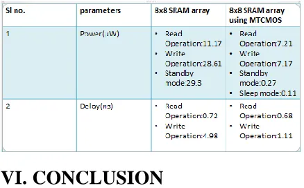
power consumption in proposed 8T double gate SRAM cell during standby mode is reduced to 0.11uW (almost 0) which is quite better than compare to 8T double gate SRAM cell as shown in fig 13.
Available online:
https://edupediapublications.org/journals/index.php/IJR/
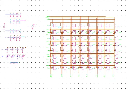
P a g e | 737Depending upon the above cells, 1x8 and 8x8 SRAM memory array is design. The proposed 8T double gate SRAM provides the significantly less power and delay.
Figure 4: Schematic of 1x8 SRAM Array.
Figure 5: Schematic Of 1x8 SRAM Array using MTCMOS.
Figure 6: Schematic of 8x8 SRAM Array.
Figure 7: Schematic of 8x8 SRAM Array using MTCMOS.
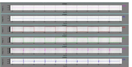
Fig 8: Waveform of 8T SRAM during Read Operation.
Available online:
https://edupediapublications.org/journals/index.php/IJR/
P a g e | 738Figure 10: Waveform of 8T SRAM during Standby Mode Operation.
Figure 11: Waveform Of 88T SRAM Using MTCMOS During Read Operation.
Figure 12: Waveform of 8T SRAM Using MTCMOS during Write Operation.
Figure 13: Waveform of 8T SRAM using MTCMOS during Standby Mode Operation.
Figure 14: Waveform of 8T SRAM using MTCMOS during Sleep Mode Operation.
V. Performance Analysis
A) Average power consumption of double gate SRAM cells during WRITE mode
Available online:
https://edupediapublications.org/journals/index.php/IJR/
P a g e | 739Figure 15: Average power Consumptions of the Double Gate SRAM Cells during Write Mode at T=90.
B) Average power consumption of double gate SRAM cell during READ mode
Table 2: Average power consumption during read operation.
Figure 16: Average Power Consumptions of the Double Gate SRAM Cells during Read Mode at T=90.
C) Delays of Double Gate SRAM cell during WRITE Mode
Table 3: Delay during write operation.
Figure 17: Write Delays of the Double Gate SRAM Cell at T=90.
D) Delays of Double Gate SRAM Cell during READ Mode
Available online:
https://edupediapublications.org/journals/index.php/IJR/
P a g e | 740Figure 18: Read Delays of the Double Gate SRAM Cell at T=90.
E) Comparison of 1x8 SRAM and 8x8Array SRAM with and without MTCMOS.
Table 5: comparison of 1x8 Array SRAM
Table 6: Comparison of 8x8 Array SRAM
VI. CONCLUSION
The proposed design of 8T MTCMOS SRAM cell consume less power and provide high speed operation in all three modes of operation (i.e. read, write, standby mode). The proposed design
provide low power solution in high speed
devices like laptops, mobile phones
programmable logic devices etc. when they are in Standby mode. The simulation results shows that power consumption and dissipation is less for proposed 8T double gate SRAM cell using MTCMOS. Similarly 16x16, 32x32 and higher order memory can be design to reduce power and delay.
REFERENCE
[1] E. Seevinck et al., “Static-Noise Margin Analysis of MOS SRAM Cells,” IEEE J.Solid-State Circuits, vol.SC-22, no.5 pp.748-754, Oct. 1987.
[2] Benton H. Calhaun, Anantha P.
Chandrakasan “Static Noise Margin Variation for Sub-threshold SRAM in 65 nm CMOS”, IEEE Journal of Solid-State Circuits,, pp.1673-1679. vol.41,July 2006.
[3] Hailong JIAO, Noise Mitigation in Low Leakage MTCMOS Circuits, DEC 2012.
[4] Wenxin Wang, Low power Multi Threshold CMOS circuit optimizations and CAD Tool design, May 2004.
[5] Arandilla,C.D.C et al.“Static Noise Margin of 6T SRAM Cell in 90-nm CMOS” IEEE 13th International Conference on computer modeling and Simulation, pp.534-539,March 30,2011. [6] E. Grossar “Read Stability and Write-Ability Analysis of SRAM Cells for Nanometer
Technologies”, IEEE J.Solid-State
Circuits,vol.41,no.11 ,pp. 2577-2588,Nov. 2006.
[7] Shairfe Muhammad Salahuddin., et al., “Eight-FinFET Fully Differential SRAM Cell
withEnhanced Read and Write Voltage
Margins”, IEEE TRANSACTIONS ON
Available online:
https://edupediapublications.org/journals/index.php/IJR/
P a g e | 741[8] S. Nakata et al.,“Increasing Static Noise Margin of Single-bit-line SRAM Lowering Bit-line Voltage during Reading”.IEEE 54th International Midwest Symposium on Circuits and Systems 2011.pp.1-4,7 Aug,2011.
[9] K. Takeda et al., “A Read-Static-Noise-Margin- Free SRAM Cell for Low-VDD and High-Speed Applications,” IEEE J.Solid-State Circuits,vol.41, no.1 pp.113-121, Jan., 2006.
[10] Do Anh-Tuan et al., “A 8T Diffrential SRAM With Improved Noise Margin for Bit-Interleaving in 65nm CMOS,” IEEE transactions on circuits and systems, vol.58, no.6,pp.1252-1263, June 2011.
[11] S.Birlaeta.l.“Static Noise Margin Analysis
of Various SRAM
Topologies”IACSIT,pp.303,sssss309,vol.3,No.3, june 2011.
Author profiles:
Mohammed Imad Uddin
completed his B.E in 2014 from Swathi Institute of Tech & Sci., Affiliated to Osmania University and pursuing M.E (2015-2017) in Embedded System & VLSI Design from MVSR Engineering College, Affiliated to Osmania University, Hyderabad, India. His area of interest includes Low Power VLSI and Satellite Communication.
E-mail id: [email protected]
E.V.Nagalakshmiis current- ly working as Assistant Professor in Department of Electronics &Communicati-on Engineering since 2006 in MVSR Engineering College
with a total teaching
experience of 14 years. She received her Master’s degree from College of
Engineering, Osmania University. She is pursuing her Ph.D. from Osmania University, Hyderabad, India. Her area of interest includes Low power VLSI, Digital Electronics and Microwave Engineering.