Design of a Novel Reversible ALU using an Enhanced
Carry Look-Ahead Adder
*K.JYOTHI **Md.ASIM IQBAL
*M.TECH Dept Of ECE, KAKATHIYA UNIVERSITY OF ENGINEERING AND
TECHNOLOGY
**Asst. prof Dept of ECE, KAKATHIYA UNIVERSITY OF ENGINEERING AND
TECHNOLOGY
Abstract
—
Reversible logic is gainingsignificant consideration as the potential
logic design style for implementation in
modern nanotechnology and quantum
computing with minimal impact on physical
entropy. Recent advances in reversible logic
allow schemes for computer architectures
using improved quantum computer
algorithms. Significant contributions have
been made in the literature towards the
design of reversible logic gate structures and
arithmetic units, however, there are not
many efforts directed towards the design of
reversible ALUs. In this work, a novel
programmable reversible logic gate is
presented and verified, and its
implementation in the design of a reversible
Arithmetic Logic Unit is demonstrated.
Then, reversible implementations of
ripple-carry, carry-select and Kogge-Stone carry
look-ahead adders are analyzed and
compared. Next, implementations of the
Kogge-Stone adder with sparsity-4, 8 and 16
were designed, verified and compared. The
enhanced sparsity-4 Kogge-Stone adder with
ripple-carry adders was selected as the best
design, and its implemented in the design of
a 32-bit arithmetic logic unit is
demonstrated.
Index Terms – Arithmetic Logic Unit;
Carry Look-Ahead Adder; Carry-Select
Adder; Emerging Technologies; Low
Power; Nanotechnology; Reversible Logic;
Ripple-Carry Adder; Quantum Computing
I.
INTRODUCTION
LOGICAL computing devices without a
bijection between input and output states
minimal heat generation of kTln(2) joules of
energy per computing cycle [1]. This
resulting dissipated heat also causes noise
in the remaining circuitry, which results in
computing errors. Bennett showed that the
dissipated energy directly correlated to the
number of lost bits, and that computers can
be logically reversible, maintain their
simplicity and provide accurate calculations
at practical speeds [2]. Resultantly, a new
paradigm in computer design arose with the
goal of reducing the entropy increase
andsubsequent energy dissipation. Such a
logical structure must possess the same
number of inputs and outputs and a
one-toone mapping between the input and output
states. Any device designed to these
constraints is known as a reversible logic
device.
Section II, we outline the goals of
programmable reversible logic design and
some fundamental logic gates. In Section III,
a novel 5*5 programmable MG gate is
proposed that may be utilized in an
arithmetic logic unit requiring the
calculation of AND, NAND, OR, NOR,
XOR and XNOR results. In Section IV,
previous work in programmable reversible
arithmetic logic units is reviewed, and the
proposed MG gate is implemented in the
design of a novel programmable arithmetic
logic unit. In Section V, reversible adder
designs are presented for a reversible ripple
carry adder, reversible carry-select adder
and reversible carry look-ahead adder. A
reversible implementation of the carry logic
presented in the Kogge-Stone is proposed
and verified. In Section VII, the methods of
quantum cost reduction through combining
ripple-carry, carry-select and carry
lookahead implementations of the reversible
adder are analyzed, and the most effective
ALU in terms of quantum cost and delay is
selected.
II.
REVERSIBLE LOGIC
A. Programmable Reversible Design Goals
The three major design goals of reversible
logic are as follows. First, minimization of
the quantum cost – the number of 1*1 and
2*2 reversible calculations necessary to
generate the logical output [6] - will reduce
the device’s computational complexity.
Second, minimization of the delay - the
logical depth of the device [7] – will
improve the throughput of the device. Third,
reduction of the ancillary inputs and garbage
outputs - inputs and outputs not
only serve to maintain reversibility of the
device – will improve the design
space require to implement the logic A
programmable reversible logic gate is
defined in [8]
as a logic structure which possesses a
bijection between input and output states
and an equal number of inputs and outputs
wherein a subset of the inputs are fixed
select lines, and a fixed subset of the outputs
produce guaranteed logical calculations.. An
ideal programmable reversible logic gate
with j inputs and outputs has a quantity of
fixed select inputs m, fixed select outputs n,
data inputs d and propagated outputs p such
that |_ _ _| _ |_ _ _| [8]. In addition, an ideal
programmable reversible logic gate with m
select inputs may produce at maximum _ _
logical calculations on the n logical outputs
[8].
B. Fundamental Logic Gates There are
three types of fundamental 2*2 reversible
logic gates. First, the square-root-of-not
gates utilize the unitary operators to produce
reversible logic calculations. The
Controlled-V and the Controlled-V+ gates
are the two Types of square-root-of-not
gates. In both of these gates, when the
control input is 0, the second input is
propagated to
the output. The corresponding unitary
operator is propagated to the second output
when the control input is 1, where the
unitary operation is for the
Controlled-V
gate and for the
V+ gate. When two
Controlled-V gates are activated in series, they act as an
inverter. The same holds for two
Controlled-V+ gates in series. When a Controlled-V
and Controlled-V+ gate are activated in
series, they act as an identity. The second
type of fundamental 2*2 reversible-logic
gate is the Feynman gate, or the
Controlled-Not gate. Proposed in [9] by Feynman, it is
configured such that its outputs states
correlate to the input states in the following
manner: and The resulting
value of thesecond output corresponds to the
result of a conventional XOR gate. Since
fanout is expressively forbidden in
reversible logic, since a fanout has one input
and two outputs, the Feynman gate may be
used to duplicate a signal when B is equal to
0. Its quantum configuration is shown in
The third type of fundamental 2*2 reversible
logic gate is the integrated qubit gate. This
gate is implemented with a Feynman gate
with either a Controlled-V or Controlled V+
gate. The XOR output of the Feynman gate
is used as the control signal for the
Controlled-V or V+ gate it is coupled with.
The quantum cost of the integrated qubit
gate is 1 and its worst-case delay is 1. The
quantum configuration of these gates are
shown below in Fig. 3.
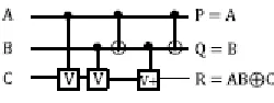
There are three 3*3 fundamental reversible
logic gates.The first was proposed in [10] by
Fredkin and Toffoli. The Fredkin gate’s
outputs states map to the inputs as follows:
and
Therefore, the outputs serve as a
multiplexed output of the two data inputs
based on the control input. It is realized
using 2 Feynman gates, a Controlled-V gate
and two integrated qubit gates. Toffoli
proposed the second fundamental 3*3
reversible logic gate in [11]. The output
states of the Toffoli gate map to the inputs in
this manner: and
The quantum cost is 5 and the worst-case
delay is 5. The quantum representation is
shown below in Fig. 5.
The 3*3 Peres gate was proposed by Peres
in [12]. The Peres gate has a quantum cost
of 4 and a worst-case delay of 3. The
quantum representation is shown in Fig. 6.
The output states map to the inputs in this
manner: and
The HNG gate, also designed by Hagparast
and Navi and proposed in [13], is a full
adder with inputs A,B,C,D producing
outputs and
and is shown in Fig. 6.
The Peres And-Or (PAOG) gate, proposed
in [8], produces the outputs
and
Fig. 7 shows the
quantum representation of the PAOG gate.
This gate is an extension of the Peres gate
for ALU realization. When the PAOG is
utilized as a programmable reversible logic
gate with two select inputs, it will calculate
four logical calculations on those two logical
The Morrison-Ranganathan (MRG) gate,
proposed in [8], has a quantum cost of 6,
since it consists of three XOR gates, 2
Controller-V and one Controller-V+ gate.
The worst-case delay of the MRG gate is 6.
The quantum representation of the MRG
gate is shown in Fig. 8 below. When the
MRG is utilized as a programmable
reversible logic gate with two select inputs,
it will calculate four logical calculations on
those two logical outputs: OR, NOR, XOR
and XNOR.
III. PROPOSED 5*5 PROGRAMMABLE REVERSIBLE MG GATE
Next, we propose the design of a 5*5
programmable reversible logic gate structure
utilized in the implementation of an ALU.
Fig. 9 shows the block diagram of the MG,
and the logical calculations based on the
programmable inputs are presented in Table
2. The cost of the MG is 7, and the
worst-case delay is 7. The design for the
programmable MG was verified and
simulated using VHDL in Xilinx 12.4.
is 24, and the worst-case delay is 16. For
nbit ALU devices, an addition cost of 2 is
incurred per bit in order to propagate S1 and
S2 to other bits. Therefore, the total cost for
an n-bit ALU is 26n-2. The MG gate is
utilized in the implementation of a novel
arithmetic logic unit based on those
proposed in [8]. The ALU, in addition to
producing Two 1-bit ALUs were proposed
in [8]. The first utilizes the MRG gate and
HNG gate to produce six logical
calculations: ADD, SUB, XOR, XNOR, OR
and NOR. The ALU has 8 inputs and 8
outputs. The inputs consist of three data
inputs (A, B and Cin) and five fixed input
select lines. The eight outputs are: A, S0, S3
and S4 propagated to the output, A _$B,
SUM, Cout, Overflow and Result. The cost
of this 1-bit ALU the same logical
calculations as the MG, is able to perform
addition and subtraction by utilizing the
HNG gate and store less-than operation. The
cost an n-bit ALU is 37n-3 and had a
worstcase delay of 4n+13. The proposed
ALU is shown in Fig. 10, and the logical
results based on the input opcodes are
presented in Table 3. The design for the
novel one-bit ALU was verified and
simulated using VHDL in Xilinx 12.4.
A. Design of Reversible Ripple-Carry and
Carry-Select Adders
In order to design the most efficient 32-bit
reversible arithmetic logic unit, we designed
and compared reversible implementation of
ripple-carry, carry-select and carry
lookahead adders. A reversible ripple-carry
adder and a reversible carry-select adder are
designed using the new ALU. The
ripple-carry adder has a cost of 40n-3 and a delay
of 4n + 13. The most-significant bit of the
ALU ties the Sum output to the SLT input of
the least significant bit, and the SLT input
for all other bits is 0. The reversible
carry-select adder uses the carry out of the first n/2
bits as the control signal to a Fredkin gate
implemented as a multiplexer, since the next
n/2 bits are calculated with both a carry-in of
0 and a carry-in of 1, which requires a cost
of 40(3n/2)-3 and a
delay of 2n + 19.
B. Reversible Kogge-Stone Cumulate Logic
Next, a reversible carry look-ahead adder
based on the Kogge-Stone adder is presented
[9]. First, a RKS Cumulate utilized in the
calculation of the carry out signal is
designed and verified. The logical structure
of the RKSC is shown in Fig. 11. The cost
of the RKSC is 14 and it has a worst-case
delay of 4. A cost and delay analysis of the
presented adders in the ALU
implementation is presented in Table 4.
The ripple-carry adder has the lowest cost,
but the highest delay. The carry look-ahead
adder has a prohibitively-high cost, but the
most-desirable delay.
C. Comparison of Reversible Ripple-Carry
and Carry- Select Adders with Sparsity
The Kogge-Stone adder may be enhanced to
reduce overhead and design complexity by
generating a carry every n-bits instead of
carryin of an n-bit ripple-carry or
carry-select adder. The number n is defined as
sparsity. This implementation was designed
and tested for sparsity-4, 8 and 16 with the
corresponding nbit ripple-carry and
carry-select adders. The cost and delay
comparison of each implementation is
shown in Table 5.
The design for each adder presented in
Table 5 was verified using VHDL in Xilinx
12.4.
VI. REVERSIBLE CARRY
LOOK-AHEAD DESIGN AND
IMPLEMENTATION IN A
REVERSIBLE ALU
A 32-bit reversible ALU utilizing a
sparsity-4 carry lookahead, adder implemented with
ripple-carry has a cost of 1656 and a delay
of 59. A 32-bit ALU utilizing a sparsity-8
carry look-ahead, adder implemented with
carry-select has a cost of 1568 and a delay
of 64. The carry-save implementation
represents a 5.3% improvement in cost over
the ripple-carry implementation, while the
ripple-carry produces a 7.8% improvement
in delay. Therefore, the modified carry
look-ahead adder with sparsity-4 implemented
with 4-bit ripple-carry addition is ideal for
implementation in the reversible arithmetic
logic unit. A 4- bit implementation of this
adder is shown in Fig. 12 below. The figure
shows the propagate and generate signal
logic for any adder which is not the
most-significant bits or the least most-significant
4-bits of adder. The least-significant adder is
different in that the LSB does not have input
propagate or generate signals, so the RKSCs
are not necessary. The mostsignificant adder
is different in that it does not need to
generate any future propagate or generate
Therefore, the HNG gates for the second,
third and fourth bit which produce the
propagate and generate signals are not
required, nor is the RKSC for the third bit.
The design for the entire 32-bit ALU was
verified
and simulated using VHDL in Xilinx 12.4.
VII.
CONCLUSION
A novel 5*5 programmable MG gate was
proposed and verified that may calculate of
AND, NAND, OR, NOR, XOR and XNOR
depending on the inputs from the
programmer. The proposed MG gate was
implemented in the design of a novel
programmable arithmetic logic unit, and its
design compared to previous work in
programmable ALU design. The novel 1-bit
ALU required only minimal increase in
quantum cost and delay due to the MG
design, which also allowed for increased
functionality for the programmer. Next, we
presented reversible implementations of
ripple carry adder, reversible carry-select
adder and reversible carry look-ahead adder.
A reversible implementation of the carry
logic presented in the Kogge-Stone was
presented and verified. Using these designs,
modified Kogge-Stone implementations of
these adders were compared in terms of
quantum cost and delay. The modified
Kogge-Stone carry look-ahead adder with
sparsity-4 implemented with 4-bit
ripple-carry addition was determined to be the
ideal design implementation in the
reversible arithmetic logic unit. This adder
was then implemented with the presented
one-bit ALU to produce an efficient 32-bit
ALU capable of addition, subtraction and all
REFERENCES
[1] R. Landauer, "Irreversibility and Heat
Generation in the Computational Process,"
IBM Journal of Research and Development,
vol. 5, 1961, pp. 183-91.
[2] C. Bennett, "Logical Reversibility of
Computation," IBM Journal of Research
and Development, vol. 17, 1973, pp.
525-532.
[3] R. Feynman, "Simulating Physics with
Computers," International Journal of
Theoretical Physics, 1982.
[4] R. Feynman, "Quantum Mechanical
Computers," Foundations of Physics, vol.
16, iss. 6, 1986,
[5] E. Fredkin and T. Toffoli, "Conservative
Logic," International Journal of Theoretical
Physics, vol. 21, 1980, pp. 219-53.
[6] T. Toffoli, "Reversible Computing,"
Technical Report MIT/LCS/TM- 151, 1980.
[7] A. Peres, “Reversible Logic and
Quantum Computers,” Physical Review, vol.
32, iss. 6, 1985, pp. 3266-3267.
[8] M. Morrison and N. Ranganathan,
"Design of a Reversible ALU Based on
Novel Programmable Reversible Logic Gate
Structures," To Appear in the IEEE
International Symposium on VLSI, 2011.
AUTHOR 1:-
*K.JYOTHI completed her
B.Tech in Dr.PAUL RAJ ENGINEERING
COLLEGE in 2014 and M.Tech completed
in KAKATHIYA UNIVERSITY OF
ENGINEERING AND TECHNOLOGY
AUTHOR 2:-
**Md.ASIM IQBAL working
as Asst. prof in Dept of ECE, KAKATHIYA
UNIVERSITY OF ENGINEERING AND