A New Memory Controller by Manchester Encoder & Linear Feedback
Shift Register by Pseudo Random Sequence Generator
Mr.S.Mohan Das
1Mr. M. Mahaboob Basha
2& Mrs. Sompalli Madhuri
31,2
Associate Professor Dept. of ECE,
3PG-Scholar Dept. of ECE, SVR Engineering College Nandyal,
Mail:
[email protected]
,
[email protected] &
[email protected]Abstract
In this paper a plenarily reused VLSI architecture of
FM0/Manchester encoding technique for
recollection application has been proposed. In this
paper we are encoding the 1 bit data into 16 bit data
and storing it into a recollection of certain address
location given by the linear feedback shift register
(LFSR),whose input is taken from the pseudo
arbitrary sequence engenderer (PRSG). The encoded
16 bit data is stored into recollection controller; the
encoded data is decoded back into 1 bit data under
the condition: when MSB bit is at logic state 1. By
utilizing FM0/Manchester encoding and decoding
technique, the data will be secure; this process is
facile and more expeditious to carry out. This paper
develops a plenarily reused VLSI architecture, and
additionally exhibits an efficient performance.
Keywords:FM0/ Manchester encoder, Linear
feedback shift register (LFSR), Pseudo random
sequence generator (PRSG), Memory controller.
1. Introduction
The FM0/Manchester encoding has many
applications, such as dedicated short Range
communication, Digital signal processing,
Recollection applications etc. Firstly in DSRC
application, the FM0/Manchester encoding utilizing
kindred attribute oriented logic simplification
(SOLS) technique was utilized. DSRC is a protocol
for one or two way medium ange communication.
DSRC is categorized into two types1. Automobile to
Automobile.
2. Automobile to Roadside.
In automobile to automobile, DSRC
provides the means of sending the message
and transmitting among the automobiles for
safety issues public information
announcement.
In automobile to roadside, DSRC
emphasizes on the intelligent transportation
service, such as electronic toll collection.
Here, in this paper we are utilizing FM0/Manchester
encoding technique for recollection applications.
Here the FM0 encoder encodes the 1 bit data into 16
bit and stores in certain recollection location
allocated by LFSR. The encoded data is decoded
back into 1bit, by performing XOR operation of
LFSR address bits and recollection controller input
bits. When we get the MSB bit as logic state 1, then
2. Related Work
2.1 Literature Survey
1. The literature [1] proposes the plenarily reused
VLSI architecture of FM0/Manchester encoding
utilizing homogeneous attribute oriented logic
simplification (SOLS) technique for dedicated short
range communication. The SOLS technique
ameliorates the hardware utilization rate from
57.14% to 100% for both FM0 and Manchester
encodings.
2. The literature [2] proposes VLSI architecture of
Manchester encoder for optical communications.
This design utilizes the CMOS inverter and the
gated inverter as the switch to construct Manchester
encoder. It is executed by 0.35-μm CMOS
technology and its operation frequency is 1 GHz.
3. The literature [3] later supersedes the architecture
of switch in [2] by the NMOS contrivance. It is
performed in 90-nm CMOS technology, and the
maximum operation frequency is as high as 5 GHz.
4. The literature [4] evolves a high-speed VLSI
architecture relatively plenarily reused with
Manchester and Miller encodings for radio
frequency identification (RFID) applications. This
architecture is performed in 0.35-μm CMOS
technology and the maximum operation frequency is
200 MHz
5. The literature [5] additionally proposes a
Manchester encoding architecture for ultrahigh
frequency (UHF) RFID tag emulator. This hardware
architecture is operated by the finite state machine
(FSM) of Manchester code, and is performed by
field-programmable gate array (FPGA) prototyping
system. The maximum operation frequency of this
architecture is about 256 MHz
6. The literature [6] proposes the identical design
methodology which is applied individually to
construct FM0 and Miller encoders additionally for
UHF RFID Tag emulator.
2.2 Main Theme of this Paper
The diversity between FMO and Manchester
coding seriously limits the potential to design a
VLSI Architecture that can be fully reused with each
other. The hardware utilization place a major role in
DSRC applications. There are two technologies used
for hardware utilization in DSRC applications.
(i) Reused-Oriented Boolean Simplification (ROBS).
(ii) Similarity-Oriented Logic Simplification (SOLS).
This paper explains the design of VLSI
Architecture using SOLS technology. It consists of
two major mechanisms. (i) Compact Area with
retiming (ii) sharing of Logic Operation. The
Compact Area with Retiming that compact the area
by reducing 22 transistors in the hardwaredesign.
The Sharing of Logic Operation that achieves fully
reused hardware Architecture by combining FMO
and Manchester encodings.
2.3 Coding Criteria of FM0 and Manchester
Code:
In the following analysis, the clock signal and the
With the abovevariables, the coding principles of
FM0 and Manchestercodes are discussed as follows.
2.3.1 FM0 Encoding
Figure 1: Code word structure of FM0.
As shown in Fig. 1, for all the values of X, the FM0
codeincludes two parts: one for first-half cycle of
CLK, A, and theother one for second-half cycle of
CLK, B. The belowmentioned three rules are used to
describe FM0 codingcriteria
1)The FM0 code has to perform the transition
between Aand B, When X is at logic-0.
2)There should not be any transition performed
between Aand B, When X is at logic-1.
3)Irrespective of X, The transition is performed with
in eachFM0 code.
Figure 2: Illustration of FM0 coding example.
An example of FM0 coding is illustrated in Fig. 2.
At cycle1, the X is logic-0; hence, a transition occurs
on its FM0code, as per the rule 1.At the beginning
for ease, thetransition is set from logic-0 to -1. As
per rule 3, a transitionis performed with in each FM0
code, so that the logic-1 isswitched to logic-0 in the
beginning of cycle 2. Then, as perthe rule 2, this
logic-level is held without any transition incomplete
cycle 2 for the X of logic-1. Thus, the FM0 code
ofeach cycle can be deduced with these three rules
specifiedearlier.
2.3.2 Manchester Encoding:
The example of a Manchester coding is illustrated in
Fig. 3. The Manchester code is deduced fromX ⊕
CLK--- (1)
The Manchester encoding is accomplished by
performing aXOR operation of CLK and X. The
clock always possesses transition within one cycle,
and so does the Manchester codeirrespective to what
the X is.
Figure 3: Illustration of Manchester coding example.
2.4 HARDWARE ARCHITECTURE
The hardware Architecture is mainly used to
analyse the hardware utilization of both FMO,
Manchester encoder. The hardware Architecture of
Manchester encoding is simple XOR operation. But
it is very difficult to construct hardware Architecture
FMO hardware Architecture should start with FSM
of FMO.
TABLE -I
HUR OF FMO AND MANCHESTER
ENCODINGS
Coding Active
Components(transistor count)
/ Total
Components(transistor
count)
HUR
FMO 6 (86) / 7 (98) 85.71%
Manchester 2 (26) / 7 (98) 28.57%
Average 4 (56) / 7 (98) 57.14%
The Hardware Utilization Rate (HUR) is used to determine the hardware utilization.
HUR = A/ C X 100%
3. Implementation
Proposed Design:
These articles are implemented using HDL designer
forsynthesis and Model Sim for simulation. To give
an intentanalysis, the proposed VLSI architecture is
realized withHDL design-flows.
Figure 4: Block diagram
The above block diagram consists of 5 main blocks.
1. Encoding block.
2. Pseudo random sequence generator (PRSG).
3. Linear feedback shift register (LFSR).
4. Memory controller block.
5. Decoding block.
Functions of these Blocks
1. Encodingblock:
Here in this block it consists of 4 modules
of FM0 encoder, X bit is the input given to
all the 4 modules. Inputs to this block are X
bit,clk, clr, and mode.
Figure 5: FM0 encoder modules.
Here the 1 bit input data is encoded into the 16 bit
data andsent to the memory controller block
2. Pseudo Random Sequence Generator:
It is an algorithm for generating a sequence of
numbers whose properties approximate the
properties of sequences of random number. Here it
generates sum random 4 bit numbers and sends it to
linear feedback shift register (LFSR).
3.Linear Feedback Shift Register (LFSR): LFSR
gives theaddress location where the 16 bit encoded
data has to bestored in memory controller. The
address location to the LFSR,where encoded data
has to be stored.
4.Memory Controller: In memory controller:
Firstly the 4 bitencoded data from 4 modules of FM0
encoder areconcatenated into 16 bit encoded data.
This 16 bit encodeddata is stored into a particular
address location sent byLFSR.
5. Decoding block:
Now the 16 bit encoded data stored inmemory is
XOR with the address location of LFSR. If theMSB
bit of the XOR output is at logic 1, then in only
thatcondition the data will be decoded back into 1
bit, becausethat is the condition we have designed
for.
4. Experimental Work
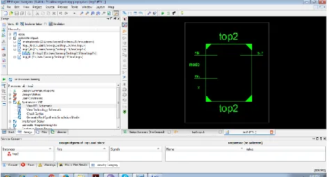
Here the block diagram shown in the fig 4 is
simulated usingModelsim and by giving the
following data as inputX= 1, Clock = clock,
Clear=1, Mode = 1, Memory input=1010
We obtain the following results shown in below
figures
Figure 7: Experimental Results 1
Here from the above figure 7, by analysing the data
LFSR out = 0011010111011010 and
Memory input= 0001010010010100.
Now by performing the XOR operation we get the
output ofMemory controller =
0010000101001110.As the MSB bit ofthis 16 bit
data is 0, the encoded data is not decoded.
5. RESULT ANALYSIS
By comparing this paper with previous
papers this paperis implemented in two different
types of design flows.
(I) fullcustom design flow.
(ii)FPGA design flow.
The full custom is realized in the literature [1],[2]
and The FPGA designflow is designed in literature
Full Custom Design Flow
With 0.18μm 1P6M CMOS technology the
design of full custom design flow dine by Taiwan
Semiconductor Manufacturing Company
(TSMC).the full custom design flow is simulated by
Tanner EDA simulation tool.
FPGA Design Flow
The design flow of FPGA is realized by
XILINX development board is shown in Fig. The
signal transition is not aligned to positive and
negative edge trigger of both encodings. The
synchronization of FPGA is achieved by two sets of
clock signals are used as CLKEXT, CLKINT .the
frequency of CLKEXT is more efficient than
CLKINT .Because the frequency of CLKEXT is
twice fast as CLKINT. The synchronization of every
signal inside FPGA is done by CLK EXT and the
manipulation of FMO, Manchester code is done by
CLKINT.
6. Conclusion
The plenarily reused VLSI Architecture of
FM0/Manchester encoder for recollection
applications is efficacious and puissant in securing
the data, as compared to the other encoding
techniques.FM0/Manchester encoder are facile to
perform operations and more expeditious. Hence
these encoding techniques are efficient.
6. References
[1] Fully Reused VLSI Architecture of
FM0/ManchesterEncoding Using SOLS Technique
for DSRC ApplicationsYu-Hsuan Lee, Member,
IEEE, and Cheng-Wei Pan
[2] P. Benabes, A. Gauthier, and J. Oksman, “A Manchestercode generator running at 1 GHz,” in
Proc. IEEE, Int.Conf. Electron., Circuits Syst., vol.
3. Dec. 2003, pp.1156–1159.
[3] A. Karagounis, A. Polyzos, B. Kotsos, and N.
Assimakis,“A 90nm Manchester code generator with CMOSswitches running at 2.4 GHz and 5 GHz,” in
Proc. 16thInt. Conf. Syst., Signals Image Process.,
Jun. 2009, pp. 1–4.
[4] Y.-C. Hung, M.-M. Kuo, C.-K. Tung, and S.-H.
Shieh,“High-speed CMOS chip design for Manchester andMiller encoder,” in Proc. Intell. Inf.
Hiding MultimediaSignal Process., Sep. 2009, pp.
538–541.
[5] M. A. Khan, M. Sharma, and P. R.
Brahmanandha, “FSMbased Manchester encoder for UHF RFID tag emulator,”in Proc. Int. Conf.
Comput., Commun. Netw., Dec. 2008,pp. 1–6.
[6] M. A. Khan, M. Sharma, and P. R.
Brahmanandha, “FSMbased FM0 and Miller encoder for UHF RFID tagemulator,” in Proc. IEEE