DESIGN AND ANALYSIS OF SUB 1-V BANDGAP
REFERENCE (BGR) VOLTAGE GENERATORS
FOR PICOWATT LSI’s.
Shivam Mishra
1, K. Suganthi
21
Research Scholar in Mech. Deptt, SRM University,Tamilnadu
2
Asst. Professor, Deptt. Of ECE, SRM University,Tamilnadu (India)
ABSTRACT
A bandgap reference (BGR) and sub1V BGR circuits for Picowatt LSIs is proposed here. The circuits pertains
pico-ampere current reference circuit, a bipolar transistor, and proportional-to-absolute-temperature (PTAT)
voltage generators. The circuits neglect resistors and contain only MOSFETs and one bipolar transistor. As the
sub-BGR circuit divides the output voltage of the bipolar transistor without resistors, it can operate at a sub1V
supply. Experimental results obtained in the 90nm CMOS technology depicts that the BGR circuit could generate
a reference voltage of 1.094 V and the sub-BGR circuit could generate one of 0.549 V. The power dissipations of
the BGR and sub-BGR circuit corresponds to 8.466 PW and 3023 PW.
Keywords: (Sub) Bandgap Reference, Low Voltage, Large Scale ICs (LSI), Multi-Threshold Devices,
Picowatt.
I INTRODUCTION
The objective of this paper is to design picowatt LSIs that will lead the next generation power efficient applications
like wireless sensor networks, metrological sensors, life-assist medical devices. Since they must operate for a long
time with less-than-ideal energy supply from micro-batteries, we thus require the LSIs such designed that operate
with extremely low power dissipation. To develop such LSIs, we must first develop voltage reference circuits
because they are the building blocks of most analog circuits. Bandgap reference (BGR) circuits are widely used in
modern LSIs to generate a reference voltage on chips. Here, we describe process, voltage, and temperature (PVT)
variation-tolerant voltage reference circuits that can operate at several tens of picowatts or even less. The
base-emitter voltage VBE of the bipolar transistor is accepted by voltage divider circuit which generates a sub1V
reference voltage in combination with the PTAT voltage generators. Although several BGRs have been developed
until now, still the power dissipations of most of them exceeds picowatt power units [1]–[2] and have not been
used to generate current or voltage to control the temperature characteristics of the output reference voltage [1]–[3].
We use a moderate value for resistance, still a sufficient current for the resistors is required and therefore , power
dissipation cannot be reduced. Although it can be reduced if we use a large value for resistance, but then the
resistors will occupy a large silicon area which is not considered fruitful. Our circuit avoids the usage of resistors
and contains only MOSFETs and one bipolar transistor. A resistor-less voltage reference circuits that operates at
picowatt power have been used. The proposed BGR consists of a pico-ampere current reference circuit, a bipolar
transistor, and proportional-to-absolute-temperature (PTAT) voltage generators. Because the circuit only consists of
MOSFETs except for the bipolar transistor, it can generate a bandgap voltage without resistors. In addition, a
sub-BGR circuit that generates voltage lower than 0.549 V is also presented. The proposed sub-sub-BGR uses a voltage
divider. The voltage divider accepts the base-emitter voltage of the bipolar transistor and generates a sub1V
reference voltage in combination with the PTAT voltage generators. Therefore, the proposed sub-BGR is useful as a
reference circuit in sub1V LSIs. Any additional devices, such as passive resistors, are not anymore needed in the
circuit. For the robust operation of the circuit, we used pico-ampere current reference circuit that is tolerant to PVT
variations. Section II of this paper describes the operating principles of our proposed circuits. Section III describes
the implementation of both circuits using 90nm CMOS process technology and presents the experimental results by
comparing it with experimental results of 180nm CMOS process technology. An extremely low power dissipation of
8.466 PWfor the BGR and 3023 PW for the sub1V BGR were achieved. Section IV concludes the paper.
II
OPERATING PRINCIPLES
2.1 Current in Subthreshold Region
The subthreshold current I, can be expressed as
I = KI0 exp ((VGS−VTH)/ηVT ) , (1)
where K (= W/L) is the aspect ratio of a transistor, I0 (= μCOX(η−1)V2T) is the pre-exponential factor of the
subthreshold current, μ is the carrier mobility, COX is the gate-oxide capacitance, VT (= kBT/q) is the thermal voltage,
kB is the Boltzmann constant, T is the absolute temperature, q is the elementary charge, VTH is the threshold voltage,
and η is the subthreshold slope factor. Note that, we assumed that η is a constant parameter. However, it is not
constant in actual devices and depends on gate-oxide and capacitances of depletion-layer [4]. This must be taken
into account in high-accuracy applications.
2.2 BGR
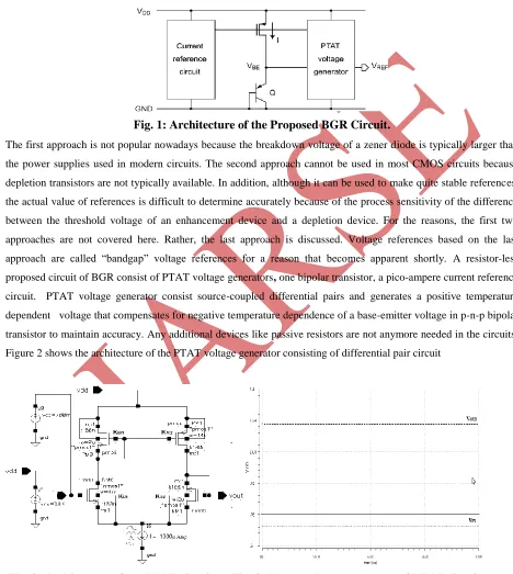
Figure 1 shows the architecture of the proposed BGR circuit.
Bandgap Voltage References find its applications in data acquisition systems. Ideally, this block will supply a fixed
dc voltage of known amplitude that does not change with temperature. There have been number of approaches that
have been taken to realize voltage references in integrated circuits. These include:
2. Making use of difference in the threshold voltage between an enhancement transistor and a depletion transistor.
3. Cancelling the negative temperature dependence of a pn junction with positive temperature dependence from a
PTAT (proportional-to-absolute- temperature) circuit.
Fig. 1: Architecture of the Proposed BGR Circuit.
The first approach is not popular nowadays because the breakdown voltage of a zener diode is typically larger than
the power supplies used in modern circuits. The second approach cannot be used in most CMOS circuits because
depletion transistors are not typically available. In addition, although it can be used to make quite stable references,
the actual value of references is difficult to determine accurately because of the process sensitivity of the difference
between the threshold voltage of an enhancement device and a depletion device. For the reasons, the first two
approaches are not covered here. Rather, the last approach is discussed. Voltage references based on the last
approach are called “bandgap” voltage references for a reason that becomes apparent shortly. A resistor-less
proposed circuit of BGR consist of PTAT voltage generators, one bipolar transistor, a pico-ampere current reference
circuit. PTAT voltage generator consist source-coupled differential pairs and generates a positive temperature
dependent voltage that compensates for negative temperature dependence of a base-emitter voltage in p-n-p bipolar
transistor to maintain accuracy. Any additional devices like passive resistors are not anymore needed in the circuits.
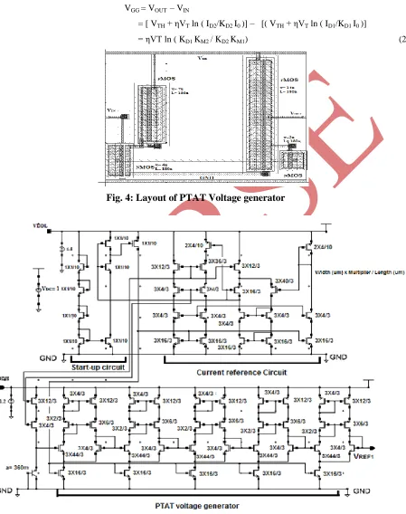
Figure 2 shows the architecture of the PTAT voltage generator consisting of differential pair circuit
When the MOSFETs operate in the subthreshold region, gate-to-gate voltage VGG in this circuit can be expressed
from (1) as
VGG = VOUT – VIN
= [ VTH + ηVT ln ( ID2/KD2 I0 )] – [( VTH + ηVT ln ( ID1/KD1 I0 )]
= ηVT ln ( KD1 KM2 / KD2 KM1) (2)
Fig. 4: Layout of PTAT Voltage generator
To operate the circuitsrobustly, we used a pico-ampere current reference circuit that is tolerant to PVT variations.
We ignore the gate and substrate leakage currents since they are negligible when compared to sub-threshold current.
Therefore, the bandgap voltage of silicon can be obtained by designing aspect ratios in the source-coupled pairs. The
bipolar transistor accepts the current through a current mirror and generates a base-emitter voltage, which is
expressed as
VBE = VT ln (IS + I)/ IS (3)
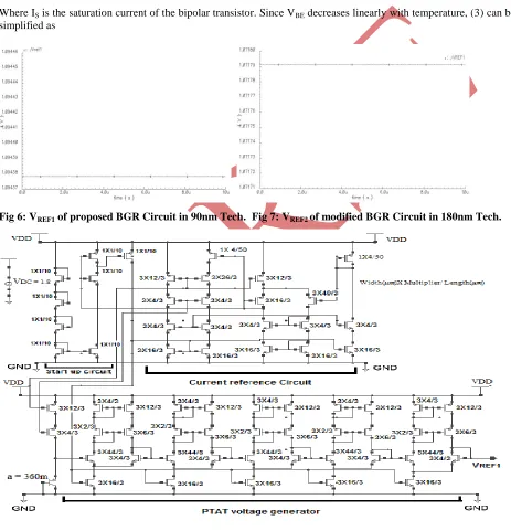
Where IS is the saturation current of the bipolar transistor. Since VBE decreases linearly with temperature, (3) can be
simplified as
Fig 6: VREF1 of proposed BGR Circuit in 90nm Tech. Fig 7: VREF2 of modified BGR Circuit in 180nm Tech.
Where VBGR is the bandgap voltage of the silicon (~ 1.2 V) and ƴ is the temperature coefficient of VBE. Because VBE
has a negative dependence on temperature, the PTAT voltage generator is used to cancel out this dependence. Since
VBE has a higher order dependency on temperature. So, there will be nonlinearities in the output voltage even though
we cancel out the negative dependence of VBE on temperature. The PTAT voltage generator in Figure 2 supplies
voltage which has a positive dependence on temperature. But, since KD1KM2 / KD2KM1 is included in a logarithmic
function, it must have a large value in order for the positive temperature coefficient of VGG to cancel out the negative
temperature dependence of base-emitter voltage VBE. Moreover, making the product of KD1KM2 much larger requires
a large area and which cannot be made use of efficiently. We, thus use a number of differential pairs in cascade
configuration to obtain sufficient PTAT voltage. When the differential pairs are connected in a cascade, total
gate-to-gate voltage VGG can be expressed as
(5)
Where N is the number of differential pairs. Output reference voltage VREF1 in the bandgap voltage reference circuit
can be expressed from (4) and (5) as
(6)
Therefore, the condition VREF1 equals to VBGR can be attained by appropriate choice of the aspect ratios of the
transistors in the differential pairs and current mirrors and of N. Also multi-threshold (MTCMOS) voltage supplies
are provided to the BGR circuit by applying different bias voltages to base/bulk terminal so as to optimize the
power. Although, the low threshold devices cause faster switching but it causes static leakage power. The high
threshold devices cause ten times reduction in static leakage power.
2.3
SUB BGR
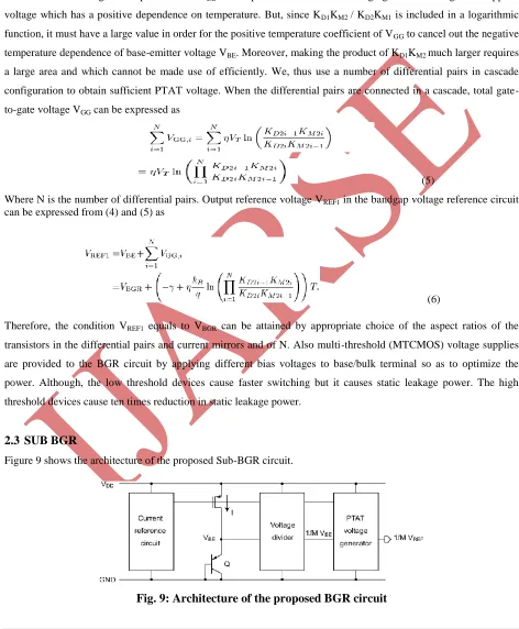
Figure 9 shows the architecture of the proposed Sub-BGR circuit.
Here, we present a voltage reference circuit that operates at sub1V power supply. This sub-BGR circuit uses an
extra voltage divider block. The voltage divider circuit divides the base-emitter voltage VBE. The output voltage
VBE/Mof the voltage divider can be expressed as
VBE /M = VBGR/M – ƴ/M T (7)
where M is the division ratio of the divider. The PTAT voltage generator is also used to cancel the negative
dependence on temperature of VBE/M. The reference output voltage of this circuit is expressed as
(8)
where N´ is the number of differential pairs. Note that because base-emitter voltage VBE is divided by M, the
negative temperature coefficient is also divided by M. Hence, the required PTAT voltage decreases and the number
of differential pairs are also reduced as compared to BGR circuit. Thus, both the area and the current dissipation in
the sub-BGR circuit are less than those in the BGR circuit. A zero temperature coefficient voltage is obtained by
designing the aspect ratios so that the second term in (8) becomes zero and the voltage can be rewritten as
VREF2 = VBGR / M (9)
III EXPERIMENTAL RESULTS
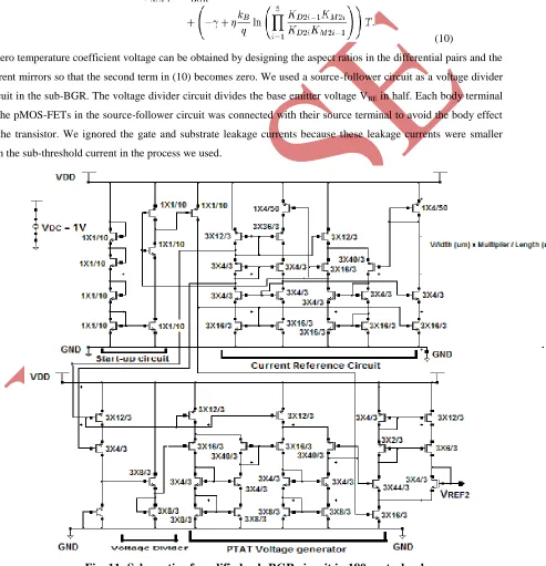
Figure 5 and 10 shows the schematics for the proposed BGR and sub-BGR circuits with all transistor sizes. As
explained earlier, cascode configuration was used in the circuits to reduce dependence on supply voltage. Five
differential pairs were used in this BGR design. The reference output voltage VREF1 of this circuit can be expressed
as
(10)
A zero temperature coefficient voltage can be obtained by designing the aspect ratios in the differential pairs and the
current mirrors so that the second term in (10) becomes zero. We used a source-follower circuit as a voltage divider
circuit in the sub-BGR. The voltage divider circuit divides the base emitter voltage VBE in half. Each body terminal
of the pMOS-FETs in the source-follower circuit was connected with their source terminal to avoid the body effect
of the transistor. We ignored the gate and substrate leakage currents because these leakage currents were smaller
than the sub-threshold current in the process we used.
The output voltage VBE/2 of the source-follower circuit can be expressed as
VBE/2 = VBGR/2 – ƴ /2 T (11)
Then, three differential pairs were used in the sub-BGR to cancel the negative dependence on temperature of VBE/2.
We used two pMOS differential pairs as first PTAT voltage generators because VBE/2 would have been too low to
apply an nMOS PTAT generator. The reference output voltage VREF2 of this circuit can be expressed as
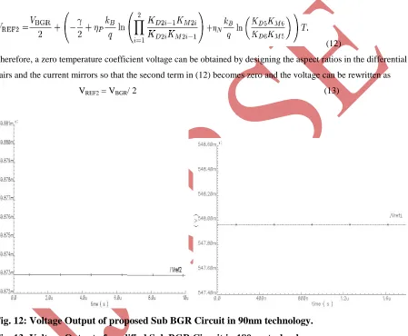
(12)
Therefore, a zero temperature coefficient voltage can be obtained by designing the aspect ratios in the differential
pairs and the current mirrors so that the second term in (12) becomes zero and the voltage can be rewritten as
VREF2 = VBGR/ 2 (13)
Fig. 12: Voltage Output of proposed Sub BGR Circuit in 90nm technology.
Fig. 13: Voltage Output of modified Sub BGR Circuit in 180nm technology
3.2 RESULTS
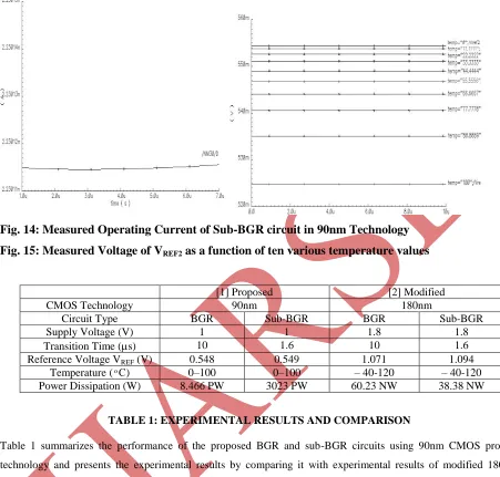
Figure 14 plots the measured operating current in the current reference circuit as a function of VDD for sub-BGR
circuit in 90nm technology. The circuit operates at 1V power supply The BGR circuit generated VREF1 as 1.09 V at
more than 1.2 V power supply. The sub-BGR circuit could operate at sub1V power supply (i.e., 0.7 V) and VREF2
was 0.549 V. Figure 15 plots the measured voltages of VREF2 as a function of temperature from 0ͦ C to 100ͦ C for
Fig. 14: Measured Operating Current of Sub-BGR circuit in 90nm Technology
Fig. 15: Measured Voltage of V
REF2as a function of ten various temperature values
[1] Proposed [2] Modified
CMOS Technology 90nm 180nm
Circuit Type BGR Sub-BGR BGR Sub-BGR
Supply Voltage (V) 1 1 1.8 1.8
Transition Time (s) 10 1.6 10 1.6
Reference Voltage VREF (V) 0.548 0.549 1.071 1.094
Temperature ( ͦ C) 0–100 0–100 – 40-120 – 40-120
Power Dissipation (W) 8.466 PW 3023 PW 60.23 NW 38.38 NW
TABLE 1: EXPERIMENTAL RESULTS AND COMPARISON
Table 1 summarizes the performance of the proposed BGR and sub-BGR circuits using 90nm CMOS process
technology and presents the experimental results by comparing it with experimental results of modified 180nm
CMOS process technology.
3.3 Discussion
Output voltage VREF1, 1.09 V, in the experimental results was lower than the material bandgap voltage, around 1.2
V. This is because the operating current increases with temperature. If bipolar transistor accepts the constant
currents, then the VBE at absolute zero temperature were almost equal to the material bandgap voltage (~1.2 V). On
the other hand, when the bipolar transistor accepts the temperature-dependent current, then the VBE at absolute zero
temperature is not equal to the material bandgap voltage. As the operating current increases with temperature, VBE
IV CONCLUSION
BGR and subBGR circuits for Picowatt power LSIs were presented. They consist of a picoampere current
reference circuit, a bipolar transistor, and PTAT voltage generators. Because the circuits only consist of MOSFETs
except for the bipolar transistor, they generate reference voltages without resistors. As the sub-BGR circuit divides
the output voltage of the bipolar transistor, it can operate at sub1V power supply. The experimental results
demonstrate that the PTAT Voltage Generator circuit has voltage output of 1.26 V. The BGR and sub- BGR circuit
could generate a reference voltage of 1.094 V and 0.549 V respectively. The power dissipation of the BGR circuit
was 8.466 pW and that of the sub-BGR circuit was 3023 pW.
REFERENCES
[1] K. N. Leung and P. K. T. Mok, “A sub-1-V 15-ppm/ C CMOS bandgap voltage reference without requiring low
threshold voltage device,” IEEE J. Solid-State Circuits, vol. 37, no. 4, pp. 526–530, Apr. 2002.
[2] A.-J. Annema and G. Goksun, “A 0.0025 mm bandgap voltage reference for 1.1 V supply in standard 0.16 m
CMOS,” in IEEE ISSCC Dig. Tech. Papers, 2012, pp. 364–365.
[3] K. N. Leung and P. K. T. Mok, “A CMOS voltage references based on weighted for CMOS low-dropout linear
regulators,” IEEE J. Solid-State Circuits, vol. 38, no. 1, pp. 146–150, Jan. 2003.
[4] Y. Taur and T. H. Ning, Fundamentals of Modern VLSI Devices. Cambridge, U.K.: Cambridge Univ., 2002.
[5] A. Wang, B. H. Calhoun, and A. P. Chandrakasan, Sub-Threshold Design for Ultra Low-Power Systems. Berlin,
Germany: Springer, 2006.
[6] K. Ueno, T. Hirose, T. Asai, and Y. Amemiya, “CMOS smart sensor for monitoring the quality of perishables,”
IEEE J. Solid-State Circuits, vol. 42, no. 4, pp. 798–803, Apr. 2007.
[7] R. T. Perry, S. H. Lewis, A. P. Brokaw, and T. R. Viswanathan, “A1.4 V supply CMOS fractional bandgap
reference,” IEEE J. Solid-State Circuits, vol. 42, no. 10, pp. 2180–2186, Oct. 2007.
[8] T. Hirose, K. Ueno, N. Kuroki, and M. Numa, “A CMOS bandgap and sub-bandgap voltage reference circuits
for nanowatt power LSIs,” in Proc. IEEE Asian Solid-State Circuits Conf., 2010, pp. 77–80.
[9] ] K. Ueno, T. Hirose, T. Asai, and Y. Amemiya, “A 300 nW, 15 ppm/ C, 20 ppm/V CMOS voltage reference
circuit consisting of suthreshold MOSFETs,” IEEE J. Solid-State Circuits, vol. 44, no. 7, pp. 2047–2054, Jul. 2009.
[10] K. N. Leung and P. K. T. Mok, “A CMOS voltage references based on weighted for CMOS low-dropout linear
regulators,” IEEE J. Solid-State Circuits, vol. 38, no. 1, pp. 146–150, Jan. 2003.
[11] T.Hirose, Y. Osaki, N. Kuroki, and M. Numa, “Anano-ampere current reference circuit and its temperature
dependence control by using temperature characteristics of carrier mobilities,” in Proc. Eur. Solid-State Circuits