ISSN 2348 – 7968
1
Design of Low Power CMOS Adder, Serf, Modified Serf Adder
V.Dileep chowdaryP 1
P
, K. Prasad BabuP 2
P
S.Ahmed BashaP 3
P
M.SreenivasuluP 4
P
K.SudhakarP 5
P
1 ,
P
Mtech DSCE 13G31D0610, ECE, JNTUA/SJCET,
Yerrakota kurnool, Andhra Pradesh 518360, India, [email protected]
P
2
P
Assistant Professor, ECE, JNTUA/SJCET,
Yerrakota kurnool, Andhra Pradesh 518360, India,[email protected]
P
3
P
Assistant Professor ECE, JNTUA/SJCET,
Yerrakota kurnool, Andhra Pradesh 518360, India, [email protected]
P
4
P
Associate Professor ECE, JNTUA/SJCET,
Yerrakota kurnool, Andhra Pradesh 518360, India, [email protected]
P
5
P
Associate Professor & HOD ECE dept, JNTUA/SJCET,
Yerrakota kurnool, Andhra Pradesh 518360, India, [email protected]
Abstract
In microprocessor and DSP`s, addition is the most commonly used arithmetic operation and it is often one of the speed-limiting elements. Hence optimization of the adder both in terms of speed and/or power consumption should be pursued. In general, CMOS style is the best in terms of robustness and stability. The CMOS structure combines PMOS pull-up and NMOS pull-down networks to produce considered outputs. In this work SERF and modified SERF full adder topology is presented. Basic Full adder, CMOS full adder, SERF adder, Modified SERF adder, Compressor 4:2, 5:2,7:2 are designed..
Keywords:33TAdder, CMOS adder, SERF, MODIFIED
SERF, COMPRESSOR.
1.
Introduction:
Adder is the crucial block in ALU. Conventional full adder is as shown below, it uses basic AND,EXOR, OR gates for SUM and CARRY.
Full adder using gates
ISSN 2348 – 7968
2
Basic CMOS Full Adder
Fig1: cmos full adder
Fig1a: cmos full adder with inputs
Fig1b: cmos full adder with inputs
Fig1c: cmos full adder with inputs
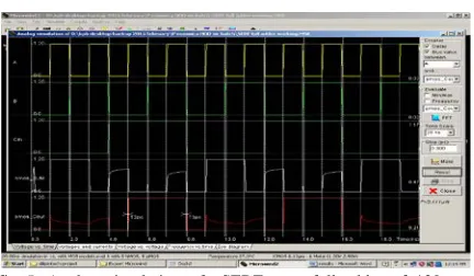
Fig1d: cmos full adder timing waveform
ISSN 2348 – 7968
3 include clock gating and dynamic voltage/frequency
scaling.
Sub threshold circuit design involves scaling the supply voltage below the threshold voltage, where load capacitances are charged/discharged by sub threshold leakage currents. Leakage currents are orders of magnitude lower than drain currents in the strong inversion regime, therefore there is a significant limit on the maximum performance of subthreshold circuits. Therefore, traditionally, subthreshold circuits have been used for applications which require ultra-low power dissipation, with low-to-moderate circuit performance [5].In the first part of this chapter, different topologies for full-adders are presented along with some circuit modifications to reduce the power consumption. Due to the importance of leakage power consumption in digital CMOS circuits, new technique is proposed to reduce the sub-threshold leakage current in high fan-in gates (e.g. OR gate) and basic block like as compressors for high-performance applications.
Energy-efficiency is one of the most required features for modern electronic systems designed for high-performance and/or portable applications. In one hand, the ever increasing market segment of portable electronic devices demands the availability of low-power building blocks that enable the implementation of long-lasting battery-operated systems. On the other hand, the general trend of increasing operating frequencies and circuit complexity, in order to cope with the throughput needed in modern high-performance processing applications, requires the design of very high-speed circuits. The power-delay product (PDP) metric relates the amount of energy spent during the realization of a determined task, and stands as the more fair performance metric when comparing optimizations of a module designed and tested using different technologies, operating frequencies, and scenarios. Addition is a fundamental arithmetic operation that is broadly used in many VLSI systems, such as application-specific digital signal processing (DSP) architectures and microprocessors. This module is the core of many arithmetic operations such as addition/subtraction, multiplication, division and address generation. As stated above, the PDP exhibited by the full-adder
would affect the system’s overall performance [1]. Thus, taking this fact into consideration, the design of a full-adder having low-power consumption and low propagation delay results of great interest for the implementation of modern digital systems. In this paper, we report the design and performance comparison of two full-adder cells implemented with an alternative internal logic structure, based on the multiplexing of the Boolean functions XOR/XNOR and AND/OR, to obtain balanced delays in SUM and CARRY outputs, respectively, and pass-transistor powerless/groundless logic styles, in order to reduce power consumption. The resultant full-adders show to be more efficient on regards of power consumption and delay when compared with other ones reported previously as good candidates to build low-power arithmetic modules.
2.
For low power circuit
implementation various reduction
are as follows:
Clock frequency reduction
Reducing the clock frequency is not as beneficial as reducing the supply voltage. However, many processors of today have different power-down modes where the clock signal is silenced to blocks of the application that are not used at the moment. This is referred to as clock gating. Clock gating can in most cases be used in conjunction with other low-power techniques.
Switched capacitance reduction
ISSN 2348 – 7968
4 i.e., correct functioning of logic gates with minimal
or near-minimal transistor sizes must be guaranteed.
Supply voltage reduction
Reducing the supply voltage is an attractive solution to reduce the power consumption since both the switched and the short-circuit power consumption have a strong VDD dependence. There are however some drawbacks with this method:A lower VDD causes longer delays.
There is an overhead in generating another lower VDD on chip.The supply voltage in state-of-the-art processes is already very low, which does not leave much margin to play with.A delay penalty can be mitigated by reducing the threshold voltage but then the subthreshold leakage will increase exponentially. The supply voltage and the choice of logic style are indirectly related through delay driven voltage scaling [28]. That is, a logic style providing fast logic gates to speed up critical signal paths allows a reduction of the supply voltage in order to achieve a given throughput. For that purpose, a logic style must be robust against supply voltage reduction, i.e., performance and correct functioning of gates must be guaranteed at low voltages as well. This becomes a
severe problem at very low voltages of around 1 V
and lower, where noise margins become critical.
Switching
activity
reduction
Switching activity of a circuit is predominantly controlled at the architectural and registers transfer level (RTL). At the circuit level, large differences are primarily observed between
static and dynamic logic styles. On the other hand,
only minor transition activity variations are observed among different static logic styles and among logic gates of different complexity, also if glitching is concerned. To reduce the power consumption Gray code can be one solution since in this code only flip one bit between consecutive numbers. Activity-based decomposition is another activity-based reduction technique
Short-circuit current reduction:
Short-circuit may vary by a considerable amount between different logic styles. They also strongly depend on input signal slopes (i.e., steep and balanced signalslopes are better) and thus on transistor sizing. Their contribution to the overall power consumption is rather limited but still not negligible (10–30%), except for very low voltages. A low power logic style should have minimal short-circuit currents and of course, no static currents besides the inherent CMOS leakage currents.
3.
Outputs
Fig1e: cmos full adder layout
ISSN 2348 – 7968
5 Fig1g: Analog Simulation of cmos full adder of 90nm technology
Fig1h: Analog Simulation of cmos full adder of 65nm technology
Fig1i: Analog Simulation of cmos full adder of 45nm technology
Fig1j: Analog Simulation of cmos full adder of 32nm technology
Results Table for CMOS full adder
0B
S.NO 1B
Foundry-Technology
2B
No. of Metals
3B
Power Dissipation
1 120nm 6 17.110µW 2 90nm 6 13.526 µW 3 65nm 6 6.295µW 4 45nm 8 1.605µW 5 32nm 8 1.190µW
When compared with various foundry technologies like 120nm.90nm,65nm,45nm, from the above table we can conclude that CMOS full adder with 32nm is having low power dissipation
.
COMPRESSORS:
4by2compressor
Fig2: 4 by 2 compressor
ISSN 2348 – 7968
6
Layout of 4 by 2 compressor
Fig2b: Layout of 4 by 2 compressor
Fig2c: Analog simulation of 4 by 2 compressor of 120 nm technology
Fig2d: Analog simulation of 4 by 2 compressor of 90 nm technology
Fig2e: Analog simulation of 4 by 2 compressor of 65 nm technology
Fig2f: Analog simulation of 4 by 2 compressor of 45 nm technology
ISSN 2348 – 7968
7 Results Table for 4 by 2 compressor
4B
S.NO 5B
Foundry-Technology
6B
No. of Metals
7B
Power Dissipation
1 120nm 6 12.182µW 2 90nm 6 11.045 µW 3 65nm 6 4.622µW 4 45nm 8 1.227µW 5 32nm 8 0.99µW
When compared with various foundry technologies like 120nm.90nm,65nm,45nm, from the above table we can conclude that 4 by 2 compressor with 32nm is having low power dissipation.
5by2 compressor
Fig3: 5 by 2 compressor
Fig3a: timing diagram of 5 by 2 compressor
Layout of 5 by 2 compressor
Fig3b: Layout of 5 by 2 compressor
Fig3c: Analog simulation of 5 by 2 compressor of 120 nm technology
7 by 2 compressor
ISSN 2348 – 7968
8 Fig4a: timing diagram of 7 by 2 compressor
Layout of 7 by 2 compressor
Fig4b: Layout of 7 by 2 compressor
Fig4c: Analog simulation of 7 by 2 compressor of 120 nm technology
SERF:
The Static Energy Recovery Full Adder (SERF) uses only 10 transistors to implement the full adder function. The design was inspired by the XNOR gate full adder design. ..In non-energy recovery design the charge applied to the load capacitance during the logic level high is drained to ground during logic level low[10]. It should be noted
that the new SERF adder has no direct path to the ground. The elimination of a path to ground reduces power consumption, removing the short circuit from the power equation. The charge stored at the load capacitance is reapplied to the control gates, the combination of not having a direct path to ground and re-application of the load charge to the control gate makes the energy – recovering full adder an energy efficient design but it has the threshold loss problem
working of SERF full adder:
SERF design uses only 10 transistors to implement a full adder.This circuit operates well at higher supply voltages, but if the supply voltage is scaled to voltages lower than 0.3V, this circuit fails to work. Table 1 shows the SERF operation with different input signals. As it can be seen, the SERF adder (Figure.3.1) is confronted with serious problems especially at lower supply voltages. Assume that one of the two input vectors ABCin=“110” and “111” are applied. As seen from Fig 3.1, when A=1 and B=1, the F node voltage is Vdd-Vth. Now if Cin=0 then Cout will be equal to Vdd-2Vth and the Sum signal is going to zero driven by a MOS transistor with its gate connected to Vdd-Vth. When Cin=1, Cout is connected to VDD (may be lower) and the SUM signal will go to Vdd-Vth. Another problem with this design is when the floating node is connected to 0 (A=0, B=1 or A=1,B=0).When Cin is “1”, Cout is charged to Vdd, but when Cin=0, Cout must be discharged to ground using a PMOS pass transistor that cannot fully discharge the output. In this case, Cout is discharged to Vtp which is higher than Vtn[11].
ISSN 2348 – 7968
9
SERF full adder
Fig5: SERF XNOR full adder
Fig5a: timing diagram of SERF XNOR full adder.
Layout of SERF xnor full adder
Fig5b: Layout of SERF xnor full adder
fig 5c:Analog simulation of SERF xnor full adder of 120 nm technology
Modified SERF
Fig6: MODIFIED SERF XNOR full adder
Fig6a: Timing diagram of modified fulladder
Layout of modified serf full adder
ISSN 2348 – 7968
10
Fig6c: Analog simulation of modified SERFfull adder of 120 nm
technology
Results table of SERF adder
8B
SERF type 9BFoundry-
technolog y 10B NO. Of Metals 11B Power Dissipation
SERF xnor full
adder 120nm 6 5.111µW Modified
SERDF xnor full adder
120nm 6 4.175µW
4. CONCLUSION & FUTURESCOPE
From the above table we conclude that modified serf xnor full adder is dissipating less power when compared with serf xnor full adder. Still low power design can be done without degradation of operation of modified serf, by using various foundry technologies.
REFERENCES
1.N. Weste and K. Eshraghian, “Principles of CMOS digital design” Reading, MA: Addison-Wesley, pp. 304–307.
2.A. P. Chandrakasan, S. Sheng, and R. W. Brodersen, “Low- power CMOS digital design,” IEEE J. Solid-State Circuits,vol. 27, pp. 473–484,Apr. 1992. D. Radhakrishnan, “Low voltage CMOS full adder cells,” Electronic letters, vol. 35, pp.1792-1794, 1999.
3.A. P. Chandrakasan and R.W. Brodersen, “Minimizing power consumption in digital CMOS circuits,” Proc. IEEE, Apr.1995, vol. 83, No. 4, pp. 498–523.
4.W. C. Athas and N. Tzartzanis, “Energy Recovery for Low PowerCMOS”, Proc. Of 16th Conference on AdvancedResearch in VLSI, 1995, pp. 415-429.
5.R. Shalem, E. John and L. K . John, “A novel low power energy recovery full adder cell”, Proc. Of the IEEE Great LakesSymposium of VLSI, Feb. 1999, pp. 380-383.
6.Yingtao Jiang, Abdulkarim Al-Sheraidah, Yuke Wang, Edwin Sha, and Jin- Gyun Chung, “A Novel Multiplexer-Based Low-Power Full Adder”, IEEE Transactions on Circuits and Systems II: Express Briefs, July 2004, Vol. 51, No. 7, , PP. 345-348.
7.H. T. Bui, A. K. Al-Sheraidah, and Y. Wang, “Design and analysis of 10- transistor full adders using novel XOR-XNOR gates,” Proc. Of Int. Conf. on Signal Processing (Wold Computer Congress), Beijing, China, Aug. 2000.
8.Y. Jiang, Y.Wang, and J.Wu, “Comprehensive power Evaluation of Full Adders,” Florida Atlantic Univ., BocaRaton,Tech. Rep., 2000
9. R. Shalem, E. John and L. K . John, “A novel low power energy recovery full adder cell”, Proc. Of the IEEE Great LakesSymposium of VLSI, Feb. 1999, pp. 380-383.
10. Yingtao Jiang, Abdulkarim Al-Sheraidah, Yuke Wang, Edwin Sha, and Jin- Gyun Chung, “A Novel Multiplexer-Based Low-Power Full Adder”, IEEE Transactions on Circuits and Systems II: Express Briefs, July 2004, Vol. 51, No. 7, , PP. 345-348.
11. H. T. Bui, A. K. Al-Sheraidah, and Y. Wang, “Design and analysis of 10- transistor full adders using novel XOR-XNOR gates,” Proc. Of Int. Conf. on Signal Processing (Wold Computer Congress), Beijing, China, Aug. 2000.