ISSN(Online): 2319-8753 ISSN (Print): 2347-6710
I
nternational
J
ournal of
I
nnovative
R
esearch in
S
cience,
E
ngineering and
T
echnology
(A High Impact Factor, Monthly, Peer Reviewed Journal) Visit: www.ijirset.com
Vol. 8, Issue 8, August 2019
Design and Analysis of 4 Bit and 8 Bit
Multiplier Using GDI and CMOS Technology
Sanchita Tongya, Rahul Sharma, Gajendra sujediya
Research Scholar, M. Tech (VLSI), RIET JAIPUR, Rajasthan, India
Assistant Professor, RIET JAIPUR, Rajasthan, India
Assistant Professor, RIET JAIPUR, Rajasthan, India
ABSTRACT: Multiplier is an arithmetic circuit that is extensively used in DSP, microprocessors and communication applications like, FFT, Digital Filters etc. Today entire world is demanding compact and small digital devices which should perform fast with low power consumption. Multiplier is the basic building block in almost all digital devices and it impacts the speed, power and area of a device significantly. Thus it is important to design an efficient multiplier which should perform fast with low power consumption. Optimizing the delay, area and power of a multiplier is a major design issues, as area and speed are usually conflicting constraints.
In this paper reconfigurable 8x8 Wallace Tree multiplier using CMOS and GDI technology is designed in 180nm. Wallace Tree multiplier is efficient in power and regularity without increase in delay and area. The idea is the generation of partial products in parallel using AND gates. The addition of partial products is reducing using Wallace Tree which is hierarchically divided into levels. Therefore there will be a significant reduction in the power consumption, since power is provided only to the level that is involved in computation and the remaining two levels switched off.
I. INTRODUCTION
With expeditious development of VLSI applications such as DSP, image, video processing and microprocessors extensively use logic gates and arithmetic circuits. Because of powered by batteries, the supply voltage is often limited, and the life time of the battery is of great importance for these devices. Therefore, the design of low voltage, low-power circuitries has become more important. Recently, building low power VLSI System has emerged as highly in demand because of the fast growing technology in mobile communication and computation. The demand for increasing speed, compact implementation and low power dissipation triggers numerous research efforts. With the scaling down of VLSI technologies, more complicate digital circuits have been implemented with a higher clock rate and lower supply voltage. However, the decreased supply voltage restricts the signal swing in circuits and brings difficulties for circuit design.
In low-voltage environments, the transistor characteristics also degrade and some circuit techniques can no longer be used, thus the low-voltage design is different from the traditional circuit design technique. Gate Diffusion input (GDI) a new technique of designing low-power digital combinational circuit. This technique allows reduction in power consumption, transistor count, propagation delay and area of digital circuits.
ISSN(Online): 2319-8753 ISSN (Print): 2347-6710
I
nternational
J
ournal of
I
nnovative
R
esearch in
S
cience,
E
ngineering and
T
echnology
(A High Impact Factor, Monthly, Peer Reviewed Journal) Visit: www.ijirset.com
Vol. 8, Issue 8, August 2019
II. BASICS OF MULTIPLIERS
Multiplication is an operation that occurs frequently in digital signal processing and many other applications. However, multipliers occupy a much larger area and incur much longer delays than adders. Therefore it is imperative that special techniques be used to speed up the calculation of the product while maintaining a reasonable area.
The product is the result of multiplying the multiplicand to the multiplier. The multiplication operation is performed in two main steps. First is the partial product formation, which consists of AND-ing each bit of the multiplier with the multiplicand. Each successive partial product belongs one place to the left of the previous partial product. The second step is partial product accumulation, where the partial products are combined to form the result.
Application of Multipliers
Used in digital signal processing operations such as filtering, convolution and analysis of frequency. Image processing.
Arithmetic units in Microprocessors.
Used in graphics and computation system.
Cryptosystems
Basic Multiplication Process
The operation of multiplication is rather simple in digital electronics. It has its origin from the classical algorithm for the product of two binary numbers. This algorithm uses addition and shift left operations to calculate the product of two binary numbers. Techniques involve computing a set of partial products, and then summing the partial products together.
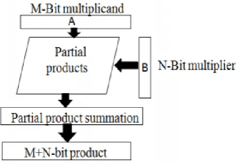
A generic block diagram of multiplier is shown in figure 1. In M × N-bit multiplication can be viewed as forming N partial products of M bits each, and then summing the appropriately shifted partial products to produce an M+N-bit result as product. Binary multiplications is equivalent to a logical AND operation. Therefore, generating partial products must be added and, if necessary, any carry values passed to the next column.
ISSN(Online): 2319-8753 ISSN (Print): 2347-6710
I
nternational
J
ournal of
I
nnovative
R
esearch in
S
cience,
E
ngineering and
T
echnology
(A High Impact Factor, Monthly, Peer Reviewed Journal) Visit: www.ijirset.com
Vol. 8, Issue 8, August 2019
Wallace/ Dadda Multiplier
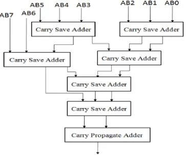
The speed of multiplier is depends on the total time taken for summation of partial products. Scientist C. S. Wallace introduced an effective way of summing the partial product bits in parallel using a tree of Carry Save Adders which generally known as the “Wallace Tree” [39].
Wallace trees are irregular in the sense that the informal description does not specify a systematic method for the compressor interconnections. However, it is an efficient implementation of adding partial products in parallel [40]. A typical Wallace tree architecture is shown in figure 2.
Fig 2: Wallace multiplier
Wallace method used three steps to multiply two numbers. These steps are Formation of the bit products.
The bit product matrix is “reduced” to a two row matrix by using a carry-save adder (also called 3:2 counters).
The remaining two rows are summed using a fast carry-propagate adder to produce the final product. Although this
ISSN(Online): 2319-8753 ISSN (Print): 2347-6710
I
nternational
J
ournal of
I
nnovative
R
esearch in
S
cience,
E
ngineering and
T
echnology
(A High Impact Factor, Monthly, Peer Reviewed Journal) Visit: www.ijirset.com
Vol. 8, Issue 8, August 2019
Disadvantage of Wallace tree Multiplier is Complex to layout and have irregular wires.
This method was further refined by Dadda to improve efficiency of addition of the partial product. The Dadda scheme essentially minimizes the number of adder stages required to perform the summation of partial products [41]. This is achieved by using full and half adders to reduce the number of rows in the matrix and number of bits at each summation stage.
2-BIT Multiplier
In 2 × 2 bit multiplier, the multiplicand has 2 bits each and the result of multiplication is of 4 bits. Hardware realization of 2 x 2 multiplier is shown in fig 3.
ISSN(Online): 2319-8753 ISSN (Print): 2347-6710
I
nternational
J
ournal of
I
nnovative
R
esearch in
S
cience,
E
ngineering and
T
echnology
(A High Impact Factor, Monthly, Peer Reviewed Journal) Visit: www.ijirset.com
Vol. 8, Issue 8, August 2019
Fig 4 : 2-Bit Multiplier
III. SIMULATION RESULTS
2-BIT MULTIPLIER
ISSN(Online): 2319-8753 ISSN (Print): 2347-6710
I
nternational
J
ournal of
I
nnovative
R
esearch in
S
cience,
E
ngineering and
T
echnology
(A High Impact Factor, Monthly, Peer Reviewed Journal) Visit: www.ijirset.com
Vol. 8, Issue 8, August 2019
2-bit CMOS multiplier is also designed. Various parameters like delay and power dissipation is calculated for both CMOS & GDI based multiplier as shown in table 1 and 2 respectively.
Table 1
Delay and Power Dissipation of 2-bit CMOS multiplier
Vdd Delay (ns) Power dissipation (mW)
1.8 0.06 1.4965
1.6 0.07 1.3773
1.4 0.08 0.7645
1.2 0.085 0.4821
1.0 0.095 0.2568
Table 2
Delay and Power Dissipation of 2-bit GDI multiplier
Vdd Delay (ns) Power Dissipation (mW)
1.8 0.02 0.729
1.6 0.055 0.520
1.4 0.070 0.307
1.2 0.075 0.165
1.0 0.085 0.095
IV. CONCLUSION
Multiplier is one of the most important components of many digital signal processing, general purpose processing, image processing and other digital application. Multiplier performance can be measured by using performance factors like Power, Delay and area. In efforts to identify the most efficient multiplier, this research makes the following conclusions.
The GDI based wallace tree multiplier occupies smaller silicon area with higher resolution than the conventional wallace tree multiplier. Various parameters like delay and power dissipation of other circuits are also calculated with respect to different power supply. Result shows that Power dissipation and delay of GDI based Wallace tree multiplier at 1.8V power supply is 8.8mW and 0.02 nS respectively and total transistor count is 912.
REFERENCES
[1] IEEE T ransactions on Very La rge Sca le Integration(VLSI)systems, by Kunal &Nidhi Kedia, Volume-1,Issue-3,2018.
[2] Pushpalata Verma ,design of 4x4 mult iplier using EDI tool.Volume 48-No.20,June 2012.
[3] Marimuthu R,Me mber ,IEEE,Elsie Re zinold Y, and P.S.Mallic k,Senior Me mber,IEEE, Design and Analysis of Multiplie r Using
Approximate 15-4 Co mpressor.DOI 10.1109-ACCESS.2016.22636128,IEEE Access.
[4] Sudeep M.C,Sharath Bimba.M,Mahendra Vucha,Design and FPGA Imp le mentation of High Speed VedicMultip lier.Volu me-90-No
16,March 2014.
[5] Shilpi Thawa it,Jagveer Ve rma , FPGA Imp le mentation of Simp le and High Speed Vedic Multiplier.Volu me-2 Issue 3 May-June 2015.
[6] SR Panigrahi,O P Das,B B Tripathy,T K Dey, FPGA Imp le metation of a 4x4 Vedic Multiplier. Vo lu me 7, Issue 1 (May 2013),pp76-80.