Abstract
AZIDEHAK, ALI. Synchronization and Architectures of Distributed Controllers in Advanced Modular Multi-Level Converters. (Under the direction of Dr.Subhashish Bhattacharya.)
In order to synchronize the distributed control system (DCS) in modular converters such as
Advanced Modular Multi-level Converters (AMMC) with the supervisory controller, a network
layer must be established, and appropriate control architecture must be designed. The thesis
covers subjects in designing modular controllers for AMMC application. The main focus will
be on engineering point of view and the practicality of the controller. In order to implement the
system, several standards has been investigated and the best one has been chosen. In the first
chapter, a brief review of the High-Voltage Direct Current (HVDC) power transfer methodology
and AMMC applications in such systems has been described and investigated. In the second
chapter, a general control architecture for AMMC has been proposed with a single controller
method. It consists of methods and algorithms to rectify the voltage, control the voltage level
and balance the voltage for each module in the system. The third chapter covers the modular
implementation of such systems with distributed controllers. It will review different network
architectures and demonstrate the implementation of DCS in AMMC. Chapter 4 contains
experimental results for both the singular and modular controller methods in detail. The results
are chosen to approve the functionality of the proposed control methods. Last chapter will make
conclusion about the entire project and give further proposal to researchers who will continue
the research. The appendix A also contains schematic design of the controller and interface
© Copyright 2014 by Ali Azidehak
Synchronization and Architectures of Distributed Controllers in Advanced Modular Multi-Level Converters
by Ali Azidehak
A thesis submitted to the Graduate Faculty of North Carolina State University
in partial fulfillment of the requirements for the Degree of
Master of Science
Electrical Engineering
Raleigh, North Carolina
2014
APPROVED BY:
Dr.Alexander Dean Dr.Srdjan Lukic
Dedication
To my parents
Fakhri Shahin & Asghar Azidehak
Biography
Ali Azidehak was born in Esfahan, Iran. During his life, experiencing new thing and researching
about new subjects, was the first priority in the life for him. It started with a junior robotic team
which participated in international competitions. He continued his dream and received his B.Sc
in Electrical Engineering from Islamic Azad University at Qazvin, Iran. During B.Sc, He has
worked in the Mechatronics Research Lab for 4 years and has participated in several Robocup
international competitions. In 2012, he started M.Sc in Electrical Engineering at North Carolina
State University Raleigh, NC. He started his research under supervision of Dr.Bhattacharya at
FREEDM systems center. During this period, he has worked on broad area of power electronics
systems. The thesis presented here is based on his research in FREEDM research center about
HVDC power transmission and improving control systems for advanced modular multi-level
Acknowledgements
I would like to thank my parents for their moral and financial support. They made it possible for
me to get my degree from NCSU.
I would like to thank Dr.Subhashish Bhattacharya, Dr.Nima Yousefpour, Dr.Babak Parkhideh
and Dr.Sungmin Kim for their academic support during the entire project.
FREEDM research center and its employees made it possible for students to reach their goals.
Thank you for your help.
Table of Contents
List of Tables . . . vii
List of Figures . . . viii
Chapter 1 Introduction . . . 1
1.1 Brief History of HVDC Power Transmition . . . 1
1.2 Proposed AMMC Architecture . . . 2
1.3 Singular vs. Modular Control . . . 3
Chapter 2 Design of an Advanced Modular Multi-Level Converter Using a Single Controller . . . 6
2.1 Control Structure for AMMC in General . . . 6
2.1.1 DC Terminal Voltage Controller . . . 6
2.1.2 Current Controller . . . 7
2.1.3 Phase Voltage Balancing Controller . . . 7
2.1.4 Module Voltage Balancing Controller . . . 11
2.2 Hardware Implementation . . . 13
2.2.1 Converter Design . . . 13
2.2.2 Sensors and Interface . . . 15
2.2.3 Controller and Complete Setup . . . 16
Chapter 3 Control and Synchronization of Distributed Controllers in Advanced Modular Multi-level Converters . . . 21
3.1 Network Design . . . 21
3.1.1 Interconnections . . . 21
3.1.2 Data Link Layer . . . 27
3.1.3 Physical Layer . . . 29
3.1.4 Synchronization . . . 32
3.1.5 Timing Considerations and Modeling . . . 37
3.2 Controller Design . . . 41
3.2.1 Processor Architecture for Modular Control . . . 41
3.2.2 Distributed Control Structure . . . 43
3.2.3 Hardware setup . . . 44
Chapter 4 Experimental Setup Results for Advanced Modular Multi-level Con-verter . . . 46
4.1 Single Controller Advanced Modular Multi-level Converter Results . . . 46
Chapter 5 Conclusion and Future Works . . . 60
5.1 Conclusion . . . 60
5.2 Future Works . . . 61
References . . . 62
Appendix . . . 63
List of Tables
Table 2.1 System Parameters for AMMC experimental test-bed . . . 20
List of Figures
Figure 1.1 Advanced Modular Multi-level Converter (AMMC) Architecture in HVDC
Power Transfer . . . 3
Figure 1.2 Schematic Diagram of H-bridge Converter used in Advanced AMMC . . . 4
Figure 1.3 Average Model of DC/DC converter . . . 4
Figure 2.1 Terminal DC Voltage Control . . . 7
Figure 2.2 Current Control Diagram . . . 8
Figure 2.3 Block Diagram of Three Module per Phase AMMC . . . 8
Figure 2.4 Phase Voltage balancing Controller block diagram . . . 11
Figure 2.5 Module Voltage Balancing Controller Block Diagram . . . 12
Figure 2.6 Back to Back H-Bridge Converter . . . 14
Figure 2.7 Schematic of Gate Driver Board . . . 14
Figure 2.8 Schematic of Power IGBT Board . . . 15
Figure 2.9 Interface Board and Sensor Board Connected to the Converters . . . 16
Figure 2.10 Analog Signal Conditioning Circuit in Interface Board . . . 17
Figure 2.11 Complimentary Signal Generator with Dead-time and Output Buffer . . . . 17
Figure 2.12 Concerto Controller Board . . . 18
Figure 2.13 The Complete Setup Platform to Test and Get Results . . . 19
Figure 3.1 Daisy-Chain Network Architecture for One Leg of AMMC System . . . 22
Figure 3.2 Two Wire RS485 Transmitter/Receiver Connection - Courtesy of Analog Device . . . 23
Figure 3.3 Parallel Network Architecture for One Leg of AMMC System . . . 25
Figure 3.4 Parallel-Daisy Network Architecture for One Leg of AMMC System . . . . 25
Figure 3.5 Data Frame Used to Send Data from Master to Slave . . . 27
Figure 3.6 Four Wire RS485 Serial Communication for AMMC . . . 31
Figure 3.7 Data Flow Diagram between Slave and Master Controllers . . . 34
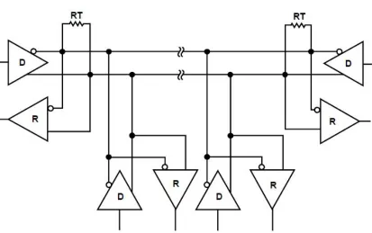
Figure 3.8 PWM Phase Synchronization Hardware Schematic in Slave Controllers . . 35
Figure 3.9 PWM Phase Synchronization Algorithm . . . 36
Figure 3.10 Performance of Control Systems versus Sampling Time . . . 37
Figure 3.11 Time Diagram Showing the Time Spend to Transfer Data Between Different Node of a Network Control System . . . 38
Figure 3.12 Waiting Time Diagram . . . 39
Figure 3.13 Signal to Controller Simulation Model . . . 40
Figure 3.14 Architecture of Concerto dual-core controller - courtesy of Texas Instrument 42 Figure 3.15 Control Block in each Module . . . 43
Figure 3.16 Modular Controller Setup for AMMC . . . 45
Figure 4.2 Phase A Current and Voltage . . . 48
Figure 4.3 Phase B Current and Voltage . . . 49
Figure 4.4 Phase C Current and Voltage . . . 50
Figure 4.5 Phase to Neutral Voltage in One Phase of Converter . . . 51
Figure 4.6 DC Voltage of Modules in Phase A . . . 52
Figure 4.7 DC Voltage of Modules in Phase B . . . 52
Figure 4.8 DC Voltage of Modules in Phase C . . . 53
Figure 4.9 DC Voltage of Output Terminal . . . 53
Figure 4.10 CSMA Data Transfer from Slave Controllers to Master Controller . . . 54
Figure 4.11 TDMA Data Transfer from Slave Controllers to Master Controller . . . 55
Figure 4.12 Grid Currents . . . 55
Figure 4.13 Voltage and Current at Phase A . . . 56
Figure 4.14 Voltage and Current at Phase B . . . 56
Figure 4.15 Capacitor DC Voltages at Phase A . . . 57
Figure 4.16 Capacitor DC Voltages at Phase B . . . 57
Figure 4.17 Capacitor DC Voltages at Phase C . . . 58
Figure 4.18 Capacitor DC Voltage at Output Terminal . . . 59
Chapter 1
Introduction
1.1
Brief History of HVDC Power Transmition
The conception of transferring power through DC line, started in late 1800 with the famous
dis-cussion between Nikola Tesla and Thomas Alva Edison. Edison Believed that DC transmission
is safer for human beings but Tesla focused on the fact that the generation and transmission
of AC power is much easier than the DC. Finally, Tesla won the discussion because of his
economical and feasible methods, and till now, AC power transmission is the dominant method
for transferring electrical power in the world[6].
Edison’s idea did not vanish in history. In the early 1930s, scientists started to do research on
wire insulators, theory of power transmission and converter systems topology. It is obvious that
with technology improvement in that time, there was no feasibility of making such system in
practice.
At the end of World War II, the need for electric power increased a lot and investigations started
again. The HVDC which we know as it is, began its development from 1954. The first systems
systems were introduced. Computer development has also helped a lot in the development of
control systems and switching signal generation. All of these developments worked together to
form Advanced MMC (AMMC) as it will be covered by this thesis.
1.2
Proposed AMMC Architecture
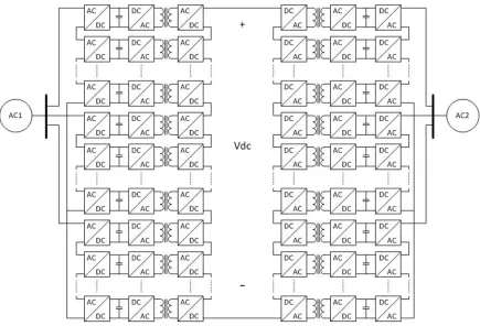
Modular Multi-Level Converter (MMC) concept has been investigated for a long time. Here, an
alternate to MMC has been proposed that will ease several design parameters. The architecture
which we are interested in is cascaded H-bride converters with isolation DC/DC converter for
each stage. As we can see in Figure 1.1, several modules have been connected in series together
and formed a single converter. The number of modules is dependent on the overall operating
voltage of the system. As an example, for a 800 kV system it can reach up to overall of 200
converters.
Figure 1.1 shows the architecture of the converter which has been used in the MTDC project.
The number of converters per phase in this project is 3 which will result in 9 total modules
in the system. Each separated module is a full-bridge converter and the dc voltage side of the
converter has been connected to a DC/DC converter.
Each module has three internal stages that work together (Figure 1.2). From the AC side
to the DC side, the first stage is a AC/DC converter. This stage act as a rectifier and charges
the capacitor connected to the DC side. The second and third stages, are DC/AC and AC/DC
H-bridge converters connected back to back. The combination is a DC/DC converter which can
act as buck or boost converter, but in this design the conversion ratio has been selected as 1:1. It
mainly act as isolation stage because of the isolation transformer in it.
The main parameter in selecting DC/DC stage is its ability in transferring power bidirectional.
Figure 1.1: Advanced Modular Multi-level Converter (AMMC) Architecture in HVDC Power Transfer
voltage is solely depended on the input voltage and the current have inverse relation with voltage
ratio (by assuming 100% efficiency).
1.3
Singular vs. Modular Control
As it is mentioned in the previous section, AMMC consist of several modules connected in
Figure 1.2: Schematic Diagram of H-bridge Converter used in Advanced AMMC
Figure 1.3: Average Model of DC/DC converter
capacitors and switches that need be measured and controlled. Transferring all the digital and
mainly analog signals to the main controller is very inefficient and in practice, it is impossible.
Therefore, for each stage a separate controller is being used to handle the data acquisition and
One of the main problems in AMMC is triggering and synchronizing the modules to get the
intended result at the output. It means the time of trigger and the duration of the trigger signal
is very important. Since there are many modules in an AMMC system, it becomes very hard
to handle switching pulses using a single controller. Therefore, it is necessary to use several
controllers in the system and use a supervisory control to synchronize the other controllers.
There are several problems in implementing such system. It is important to design the required
network architecture, processor architectures, data packet format and control algorithms. In the
following chapters, all of these questions will be answered and the implementation result will
Chapter 2
Design of an Advanced Modular
Multi-Level Converter Using a Single
Controller
2.1
Control Structure for AMMC in General
First, it is good to have a sense of control algorithms for AMMC. Basically there are four major
control loops in each AMMC system as follow:
2.1.1
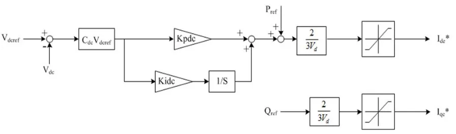
DC Terminal Voltage Controller
This controller is responsible for the entire voltage in DC link of HVDC power transfer. The
input is the link voltage and the output is dq-current that AMMC converter must supply. Since it
Figure 2.1: Terminal DC Voltage Control
2.1.2
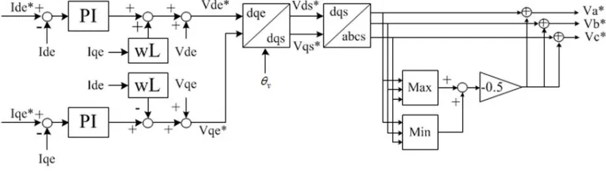
Current Controller
Unlike the terminal voltage controller, current controller has higher controller gain and therefore,
its inertia is higher. The decoupling factor has been included in the control and third harmonics
has been added to the output voltage to get the highest rail to rail output voltage in the linear
region.
2.1.3
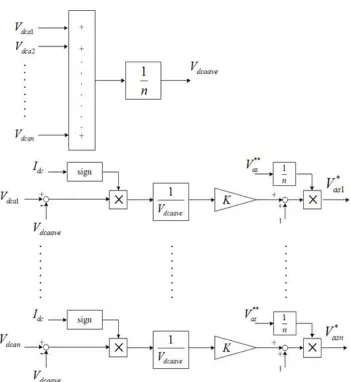
Phase Voltage Balancing Controller
It is important to have balanced voltages on DC capacitors of the converters and therefore have
balanced voltages on each phase of the converter. Phase voltage balance controllers achieve this
by adding a zero sequence to the modulating wave form and force more current in one phase.
Figure 2.2: Current Control Diagram
Figure 2.3: Block Diagram of Three Module per Phase AMMC
To understand the control theory, power equations must be written as follow:
va=Vmcos(wt)
vb=Vmcos(wt−2π/3)
ia=Imcos(wt)
ib=Imcos(wt−2π/3)
ic=Imcos(wt+2π/3) (2.2)
The power of the source would be:
Pa=vaia=0.5VmImcos(θi) +0.5VmImcos(2wt+θi)
Pb=vbib=0.5VmImcos(θi) +0.5VmImcos(2wt+θi+2π/3)
Pc=vcic=0.5VmImcos(θi) +0.5VmImcos(2wt+θi−2π/3) (2.3)
Assuming that the phase voltage balancing voltage isVpb =Vcmcos(wt+φ), the power flow
by this having this voltage is:
Pa0 =Pa+0.5VcmImcos(φ−θi) +0.5VcmImcos(2wt+θi+φ)
Pb0=Pb+0.5VcmImcos(φ−θi+2π/3) +0.5VcmImcos(2wt+θi+φ+2π/3)
Pc0=Pc+0.5VcmImcos(φ−θi−2π/3) +0.5VcmImcos(2wt+θi+φ−2π/3) (2.4)
Paavg0 =0.5VmImcos(θi) +0.5VcmImcos(θi+φ)
Pbavg0 =0.5VmImcos(θi) +0.5VcmImcos(θi+φ+2π/3)
Pcavg0 =0.5VmImcos(θi) +0.5VcmImcos(θi+φ−2π/3) (2.5)
Converting it from abc frame to dq frame the power equations are:
Pdavg0
Pqavg0
=0.5VcmIm
cos(φ−θ)
sin(φ−θ)
Now letâ ˘A ´Zs look at the voltage imbalance in phases. By finding the energy imbalance in
the phases and inject the necessary power, the voltages will become balanced too:
∆Eaavg
∆Ebavg
∆Ecavg
=CdcVpavg
∆Vaavg
∆Vbavg
∆Vcavg ⇒
∆Edavg
∆Eqavg = 2 3
1 −1 2 − 1 2 0 √ 3 2 − √ 3 2
∆Eaavg
∆Ebavg
∆Ecavg
Pd pavg∗
Pqpavg∗
=
Kp+Kis s
−∆Edavg
−∆Eqavg
Therefore, phase balancing voltage is:
The final control block diagram has been shown in the Figure 2.4. This controller can
balance the total dc voltages in each phase.
Figure 2.4: Phase Voltage balancing Controller block diagram
2.1.4
Module Voltage Balancing Controller
The last controller balances the voltages on all the DC capacitors of each module. It acts like a
circuit protector and prevents overcharging of capacitors. Just like the DC terminal controller,
the gain of this controller is low and it has high inertia.
The way this controller works is by changing the effective active cycle of each controller,
therefore the average current that each capacitor supplies will change and the circuit will become
balanced. When the grid is supplying current to the converter, the higher active duty cycle the
capacitor has, the more it is going to be charged. When the converter is sourcing current to the
Figure 2.5: Module Voltage Balancing Controller Block Diagram
2.2
Hardware Implementation
2.2.1
Converter Design
To get better understanding of the system and to prove the concept, it is required to have an
implementation of the system. The first step is to do simulation. System validation by simulations
has been accomplished by other members of the research group. The problem with the software
simulation is the speed of compilation. Another important feature is the difference between the
simulation and real-time operation. The controller is not always the same in both environments;
hence the results may not always be the same. Therefore, efforts were put on implementing the
system using hardware in the loop (HIL) tools. These tools have limited resources for simulation
and the AMMC system was not realizable by these tools too.
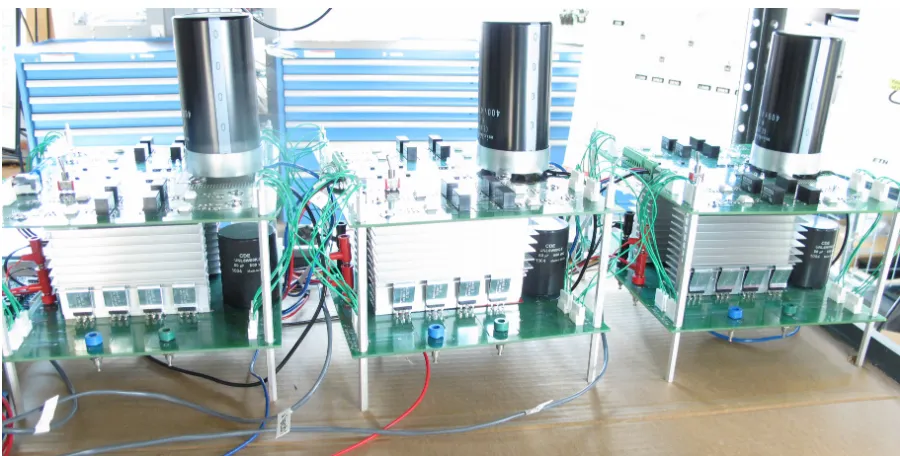
Finally, it was decided to design hardware and test the controller in the real laboratory setup. The
hardware that is being used must be fault proof (i.e. components do not burn if fault happens).
Therefore, general h-bridge converters with fault handling was used in the system (Figure 2.6).
Each converter consists of two boards which connect to each other by signal cables. The
gate driver board (Figure 2.7) gets the signals from controller, buffer it and then amplifies it for
IGBT drive purposes. It uses opto-coupling IC to isolate the power and signal circuits from each
other. The driver IC has fault protection circuit that disables the IGBT when the voltage across
collector and emitter exceed a threshold level (IGBT fault).
The power board has four legs that have common dc voltage link. Only two legs are necessary
for AC/DC conversion circuit. A large capacity (4.7 mF) must be used in DC link to increase
Figure 2.6: Back to Back H-Bridge Converter
Figure 2.8: Schematic of Power IGBT Board
2.2.2
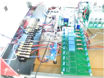
Sensors and Interface
For gathering sensory signals, an interface board has been designed. This circuit is responsible
to amplify and condition the analog signals, create and buffer the switching signals and connect
them to the appropriate connectors for the controller. All the voltage sensors have been mounted
on the sensor board to get high quality signals in compact module (Figure 2.9).
Signals that come from the sensor have±10 V range, so it must be shifted to 0-3 V range. A
limiter circuit must be considered to protect the ADC inputs of the controller from over voltages.
All of these specification have been considered in the circuit in Figure 2.10.
There are 36 switches (IGBTs) in the entire general purpose system. It is uncommon to
have such amount of PWM signal generators in controllers. Half of these switching signals
are complimentary and can be generated by analog circuits. Figure 2.11 shows the circuit that
generates complimentary signals and also applies a dead time in signal transitions (preventing
from short circuit). An output buffer has been placed at the output to decrease the fall/rise time
Figure 2.9: Interface Board and Sensor Board Connected to the Converters
2.2.3
Controller and Complete Setup
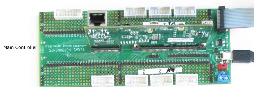
The control system in this project has to get 16 analog signal, generate 18 PWM signal and
compute control procedures in less than 10µs (PWM frequency is 10 kHz, but the deadline
to update the PWM is one tenth of the period or 10µs). Therefore, ConcertoT M 28M36 micro
controller with cutting-edge technology peripherals and dual core processor was used to handle
the control procedures. The benefit of having 2 core processor is shown in the next chapter when
Figure 2.10: Analog Signal Conditioning Circuit in Interface Board
Figure 2.12: Concerto Controller Board
Figure 2.12 shows the control board with its connection. Digital outputs have been
con-nected to the GPIOs and PWM outputs. Analog inputs have RC low pass filter to protect the
digital controller from aliasing. To debug, monitor and get result from the internal system, an
8-bit DAC was implemented in the controller board. Output of this DAC can be connected to
oscilloscope. The data that has been captured is represented in Chapter 4.
Figure 2.13 is the final assembly of converters, control and interface boards and power
management unit. The specification can be summarized in Table 2.1. This setup is based on
Table 2.1: System Parameters for AMMC experimental test-bed
Total module number (per terminal) 3 Module DC capacitor voltage 35 V
Terminal rated power 5 kVA
Chapter 3
Control and Synchronization of
Distributed Controllers in Advanced
Modular Multi-level Converters
3.1
Network Design
3.1.1
Interconnections
The architecture of the network link is based on the requirement of the system (Table 3.2).
In daisy chain structure, each converter is connected to another directly (Figure 3.1). The nearby converters can communicate fast, but since the entire process is being controlled by a
supervisory controller (master controller), this benefit cannot be utilized in the system control.
A data packet from master should travel across all converters to reach the last one. This can
cause data latency and can lead to instability in some cases. To overcome this issue, the data
being buffered in each hardware repeater. It gets even worse when PWM signal synchronization
are required to be done. Due to harmonics considerations, each PWM signal in any controller
should be synchronized to a reference time stamp and the resolution of time difference should
be in the order of sub-micro second. The added latency of signal propagation in each stage will
cause problems in the controller synchronization. Beside all these cons, the major benefit of this
architecture is its ability to be implemented by fiber optic based decoupled hardware. Since data
line is point to point, fiber optic communication is possible and this will give a high degree of
robustness to the entire design.
Figure 3.1: Daisy-Chain Network Architecture for One Leg of AMMC System
Inparallel architecture(Figure 3.3), any controller should communicate with other con-trollers in the system. Good example of this type of communication is RS-485 standard. This
communication is half duplex i.e. only one device can transmit data at any time. The pay off in
this architecture is the ability of master controller to send data packets to all of the controllers
simultaneously (Figure 3.2). Electrical precautions must be considered and twisted wire pair
should be used in transmission to avoid interference and noise issues [4].
Figure 3.2: Two Wire RS485 Transmitter/Receiver Connection - Courtesy of Analog Device
Due to the nature of parallel architecture, fiber optic realization with common industrial
devices is not possible and the only way to implement it is by electrical communication
Table 3.1: Specification of RS485 Communication
Specification RS-485
Transmission Type Differential
Maximum Cable Length 4000 ft
Minimum Driver Output Voltage ±1.5V
Driver Load Impedance 54Ω
Receiver Input Resistance 12kΩmin
Receiver Input Sensitivity ±200 mV Receiver Input Voltage Range -7 V to +12 V
No. of Drivers/Receivers per Line 32/32(256 in some versions)
architecture is the same as daisy-chain architecture and if the parallel data link gets a fault, there
is no other way to communicate with other converters and synchronize them.
To compensate the disadvantage of the latter architectures, we can implement both of the
typologies together and in the case of any fault, the other data link can be used as communication
link. The packet processing algorithm should have sufficient error checking not to send a control
Figure 3.3: Parallel Network Architecture for One Leg of AMMC System
Table 3.2: Comparison between Different Distributed Control Systems Architectures
Architecture Network Realization Advantages Disadvantages Daisy Chain (Series) Any type of serial
communication including UART, SPI, Fiber Optic
Short signal path, Scalability, Fiber Op-tic Compatibility
Data latency (from master to slave), Vulnerable data link (one connection shortage can stop the system)
Parallel One to many pro-tocols (RS-422/485, CAN, I2C)
Scalability, Broad-casting ability
Vulnerable data link (short circuit in data link can stop system functionality)
Parallel-Daisy (using both parallel and Daisy-chain)
Combination of se-rial protocols
Scalability, Broad-casting ability, Most robust
3.1.2
Data Link Layer
Choosing the right data packet format can decrease the communication time between controllers.
[7]. Based on the data that will transfer between master and slave controllers, the packet format
can be developed. It is absolutely necessary to have knowledge about timing parameters of the
communication link in real-time systems. Therefore calculation can be done about the number of
possible controllers in the grid, latency of data delivery and lead time to response to any fault [8].
Figure 3.5 is the data frame used to transmit data from master controller to the slave controllers.
The benefit of this type of data frame is that it is flexible and based on the requirement, a set
of bytes can be sent to the slave controllers. The data frame consists of data bytes that form
the packet. The start of the packet makes the slave controllers ready to receive data from the
supervisory controller. In order to make the data synchronization fault free, check sum is added
at the end of data frame (more advanced error detecting codes like cyclic redundancy check can
be implemented for higher reliability).
Figure 3.5: Data Frame Used to Send Data from Master to Slave
The number of slave controllers in a converter can be increased up to 200 modules. The data
frame must be in the most compact format to save transmission time among controllers. The
switches in each module. Each packet should also mention the module number the data belongs
3.1.3
Physical Layer
There is not a single physical network protocol that is suitable for implementation in power
electronics systems. The following parameters are important in selecting the right standard:
1- Architecture: network architecture implementation must be feasible by the protocol
2- Robustness: using either electrical or optical techniques to decrease the failure rate in packet
bits (e.g. twisted wire or fiber optic cables)
3- Speed: the higher speed the system has, the less latency between controllers which will in
turn decrease the possibility of converter instability
4- Maximum cable length: size of one AMMC can reach up to hundreds of feet and network
signal should be good at this length
5- Real time: each bit has to be transferred between controllers instantly without being buffered
6- Setup: there should be no network configuration if it restarts in the case of failure (will be
needed in fault-proof system design)
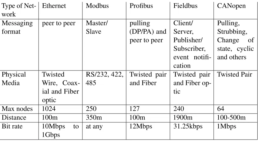
In Table 3.3, physical specification of several industrial networks has been gathered. The
information can help to select the best network protocol [1].
The finalized physical layer chosen for AMMC is four-wire RS-485 uart serial
communica-tion. This standard enables the master controller to send and receive data bidirectional and to not
stop the send operation to get response from the slave controllers Figure 3.15. The maximum
speed of the RS485 link for the communication chip that has been chosen is 5 Mbps, but to be
compatible with the international standards, 3.686 Mbps (E1 standard) is chosen for baud rate.
Data format is 8N1 and there is no parity check for each byte.
The other equivalent for this standard is Controller Area Network (CAN) bus. The reason that
this standard was not chosen is that it has static data frame and it is not flexible enough to handle
Table 3.3: Physical Specification of Industrial Network Protocols
Type of Net-work
Ethernet Modbus Profibus Fieldbus CANopen
Messaging format
peer to peer Master/ Slave
pulling (DP/PA) and peer to peer
Client/ Server, Publisher/ Subscriber, event notifi-cation Pulling, Strubbing, Change of state, cyclic and others Physical Media Twisted Wire, Coax-ial and Fiber optic RS/232, 422, 485 Twisted pair and Fiber Twisted pair and Fiber op-tic
Twisted Pair
Max nodes 1024 250 127 240 64
Distance 100m 350m 100m 1900m 100-500m
Bit rate 10Mbps to 1Gbps
3.1.4
Synchronization
Synchronization should be done for two subjects in AMMC system:
1- Data and variables which controllers have gathered and calculated
2- PWM Switching signal phase of the modular converters referenced to the supervisory
con-troller (phase synchronization)
In the first part, data is being transferred from master to slaves in the periodic manner after
computation of the control loops. Figure 3.7 shows the data flow between controllers. In the
supervisory controller, the control loop runs based on the switching frequency of the converter
(when analog signals have been converted to digital at start of PWM signal). The result is being
transferred from the control subsystem (C28) to the master subsystem (m3). This processor is
responsible to form a packet frame and send the data to the slave controllers.
The Slave controller has the same process to send/receive data and analyzing them. The
dif-ference is that the data flow from master to slave is one to many type (broadcasting), which
means sending only one packet is enough to synchronize all the slave controllers, but from
slaves to master is not the same and the channel is being shared between controllers. To divide
the channel between slave controllers, two principle solutions are available:
1- Time Division Multiple Access: The receive channel can be divided based on time division
multiple access (TDMA) technique. Whenever the master sends request to slave to get updated
data, a scheduler will start counting and based on the module number (assigned automatically or
by installer), each module sends out its status and variables. The biggest problem in this method
is the error in xtal oscillators of slave controllers and the probability of data frame overlapping.
Therefore, a dead time must be allowed between data packets to avoid this problem.
2- Carrier Sense Multiple Access: In this mode, all the slaves listen to the master controller
the master controller. The other slaves can listen to the transmitting slave and when it ends the
process, the next slave can start sending data immediately.
Due to the difference in the operating frequency of the crystal oscillators in each module
and desynchronisation of controller after each hardware fault, periodic module synchronization
is necessary for switching signals. For synchronizing the PWM wave-forms, a fast trigger signal
must be applied to all slave controllers to inform them about the reference phase. The easiest
way is to consider a separate signal line to all the modules, but it is costly and similar to having
a data link again.
The most efficient way is to using the data link to send the reference signal, but the problem is
the baud rate of the data link. Transferring single byte would take several microseconds and this
accuracy is not good enough for phase synchronization (the complete packet has several bytes
and it takes even more time). The solution is to send a data packet and make the controllers
ready to sense a transition in Rx signal and then doing the phase adjustment procedure. Figure
3.8 represent a simple hardware that can do this in the easiest way.
When the slave controllers receive the packet that makes them ready to adjust the PWM
phase, each controller should enable the phase adjustment input (low level) and wait to get
interrupt signal to load the phase value (based on module number) to the PWM counter register.
When control loop event (which is synchronized to internal oscillator and triggers at specific
times) triggers, a dummy data should be send to the serial port. The change in communication
link will trigger the entire slave controller and therefore synchronize them to the reference
phase value. Figure 3.9 show the flow chart implemented in controllers to handle signal
3.1.5
Timing Considerations and Modeling
To have better insight about the behavior of the distributed controller, timing parameters of the
system must be investigated [5]. Figure 3.10 show the performance of continuous time, discrete
time and network controlled systems in different sampling times.
Figure 3.10: Performance of Control Systems versus Sampling Time
For continuous time systems, sampling time has no meaning; therefore the performance is
more like the continuous system and therefore the quality of performance (QoP) will increase
drastically.
In Network Controlled Systems (NCS), the bandwidth of the communication link is limited.
Increasing the sampling rate means transferring more amount of data in the network that could
decrease the functionality of the system. By having knowledge about the timing in the system,
the maximum safe sampling rate can be selected for the AMMC. The rule of thumb is whenever
network bus gets crowded the performance will decrease. In the scheduled NCS, the optimum
performance can be gained by using the maximum baud rate of the network link.
Figure 3.11: Time Diagram Showing the Time Spend to Transfer Data Between Different Node of a Network Control System
Figure 3.12: Waiting Time Diagram
part of the system can be defined as follow:
1-Tpre: The time required to process control signal from the outside world in the controller
(analog to digital conversion is most important one).
2-Twait: The time that the imported data shall be buffered in the sender’s data frame until it
reaches the network link.
3-Ttx: The duration of data frame transmission from one node to another node. This delay can
be very different in master to slave and slave to master modes. The major part of theTdelayis
this part because it is out of the controller and in the network link.
4-Tpost: The delay time after data frame has been received in the destination. It consist of packet
parsing loop procedure and the delay until measured signal is used in the main control loop.
Based on the defined delays, the final delay would be:
Tdelay=Tpre+Twait+Ttx+Tpost The total delay from the signal to the control loop can be used
in modeling. The difference between single and distributed controller system is in two facts:
1- Network delay: There is always delay between measured signal to the control loop and from
2- Rounding error: Due to speed and latency requirement of the converter, variables should be
rounded to decrease the overload on the network.
Therefore, the finalized model to be used in simulation would be like Figure 3.13.
3.2
Controller Design
3.2.1
Processor Architecture for Modular Control
Handling data packets and sending the right amount of data from master controller to slave
controllers is a key parameter in designing this system. Parsing the data can take a lot of
processing power and can change the micro controller to a non real-time processor [2]. For this
problem, new processor architecture was chosen that have two processors in the same package.
One processor (ARM) is responsible for network data processing and the other one (C28) is for
control related tasks with focus on real-time applications (Figure 3.14).
By using such architecture, data can flow from network controller to real-time controller with
the minimum latency. Shared memory is a good way to synchronize such processors in the
least amount of time. The Inter Processor Communication (IPC) unit is responsible for delivery
of messages between processors and interrupting the other processor when data is ready. It is
important to use memory management algorithms such as mutual exclusion when changing
variables such that data race problems are not encountered.
The shared memory consists of two memory banks. One is assigned for master to slave data
transfer and the other one is used to transfer data from slave to master. Each bank is only writable
by one processor and is readable by all processors. The memory can be updated by application
3.2.2
Distributed Control Structure
The control procedure in each module should be in the simplest possible format. Thanks to the
cascaded control proposed in chapter two, the only control loop that needs to be implemented in
modular controllers is the module DC voltage balancing. Therefore, each module should get 2
principle variable from supervisory controller including the H-bridge voltage and the average
voltage of the DC capacitors in the system (Figure 3.15). By using the received data and the
DC capacitor voltage in the control loop, the module DC voltage balancing and H-bridge AC
voltage output can be generated.
The feedback that modular controllers give back to the supervisory controller is DC capacitor
voltage and the fault status of the switches. This feedback is used in other control loops that
need the sum of the DC capacitor voltages. The fault status can help the controller to adjust the
per module effective voltage in case some modules may have failed.
3.2.3
Hardware setup
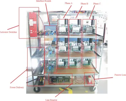
To investigate the correctness of the proposed architecture, One leg of the converter has been
implemented using distributed controllers. The converter structure and signal conditioning is
the same as single controller setup in order to compare the system results. Figure 3.15 shows
the configuration of the Concerto controller (one as master and three as slave). The result of the
setup is represented in chapter 4. Table 3.4 show the specification of modular controller based
converter setup.
Table 3.4: System Parameters for Modular AMMC experimental test-bed
Total module number (per terminal) 3 Module DC capacitor voltage 20 V
Terminal rated power 5 kVA
Chapter 4
Experimental Setup Results for Advanced
Modular Multi-level Converter
4.1
Single Controller Advanced Modular Multi-level
Con-verter Results
To validate the concept of the designed controller, hardware has been designed and experimental
results have been obtained. The results shown here is the data obtained from the output of the
measurement devices (Oscilloscope) or the integrated measurement system (Sensors) in the
controller.
Figure 4.1 shows the current that the grid provides to the converter. The controller should
manage to provide balanced current from each phase and the three phase currents should have
120 degree phase shift.
The unity power factor operation is shown in Figures 4.2, 4.3, 4.4. Each current has the same
Figure 4.1: Grid Currents
Figure 4.5 show the switching signal at the output of the AMMC. The change of the voltage
level has been completely shown in the figure.
Another important result relates to the DC voltage on each capacitor and the total DC voltage
of the terminal. Figure 4.6, 4.7, 4.8 show the DC voltages in each module and the effect of DC
voltage balancer in the control system.
The total DC voltage of the terminal is shown in Figure 4.9. There are some harmonics in
Figure 4.6: DC Voltage of Modules in Phase A
Figure 4.8: DC Voltage of Modules in Phase C
4.2
Multiple Controller Advanced Modular Multi-level
Con-verter Results
Experimental result is required to validate the discrete control system concepts in AMMC. The
hardware setup is as same as the single controller setup. Figures 4.10 and 4.11 show the TDMA
and CSMA methods to collect data from slave controllers. The CSMA is finalized to be used in
the controller.
Figure 4.10: CSMA Data Transfer from Slave Controllers to Master Controller
Figure 4.12 show the grid currents at the operating point of the converter. The requirement
for the converter is to having balanced current at each phase. This requirement is being satisfied
in the modular AMMC.
Figures 4.13 and 4.14 show the current at phase A and B. Phase A is being controlled
by modular controllers but the phase B is being controlled by a single controller. The results
Figure 4.11: TDMA Data Transfer from Slave Controllers to Master Controller
Figure 4.12: Grid Currents
Figures 4.15, 4.16 and 4.17 show the capacitor DC voltages for each phase of the converter
at the operating point of the converter.
The DC voltage at output terminal is shown at Figure 4.18. The requirement is to regulate
Figure 4.13: Voltage and Current at Phase A
Figure 4.15: Capacitor DC Voltages at Phase A
Figure 4.17: Capacitor DC Voltages at Phase C
Figure 4.18: Capacitor DC Voltage at Output Terminal
Chapter 5
Conclusion and Future Works
5.1
Conclusion
The principles of controlling Advanced Modular Multi-level Converter were investigated and a
general structure is proposed. The proposed control algorithm has been validated by
implement-ing in simplement-ingle controller architecture. The results validate the correctness of control structure for
further research.
The next effort was on network structure of the Distributed Controller System. Three different
structures proposed for arranging the modules in system and benefits of each architecture are
reviewed. Parallel architecture was chosen as the most efficient one in implementation. The
research goes in to details of this structure and how it can be implemented practically. Finally, a
prototype is designed and implemented and the result obtained to validate the system.
One of the most important factors in designing modular converters is using the correct hardware
in implementation. The module (sub-system) controller should be able to communicate with
the supervisory controller and handle the control procedures. The network structure should be
implementation.
The benefit of this research can be extended to other projects where several controller must
work synchronously to deliver power such as Modular Transformer Converter (MTC) [10]. The
converters in MTC architecture need synchronization with a supervisory controller to get data
and correctly generate the PWM signals.
5.2
Future Works
During this research, several other problems that converted in to interesting research topics were
discovered. The main subject is designing a fault-tolerant controller for AMMC that can recover
in the minimum amount of time (or even instantly) [3]. The questions that being addressed are:
1- What are the software algorithm requirements to design fault-tolerant controllers for this
power electronics application?
2- Can general purpose control cards be used to design fault-tolerant controllers?
And other questions that can be answered through the research on fault-tolerant controllers. The
research can be formed as a PhD dissertation (which author is willing to do it in the future). The
finalized system would have a fault tolerant controller connected by reliable redundant network
link through slave controllers. The number of modular controllers can be increased to make a
fully modular system in which more dynamics of the system can be investigated. Based on the
suggested model for distributed controller systems in chapter three, a simulation setup can be
designed to investigate the correctness of the controller based on PowerSim software (which
References
[1] S. Djiev. Industrial networks for communication and control.
[2] A.M. Hemeida, M. Z. El-Sadek, and S. A. Younies. Distributed control system approach for a unified power system. Universities Power Engineering Conference, 1:304–307, 2004.
[3] T. Kailath. Algorithms and architectures for high speed signal processing. Information Systems Lab, Department of Electrical Engineering, Stanford University, 1990.
[4] FANG Kun, WANG Yu, and MENG Junxia. Architecture design and analysis of a distributed test and control system based on new power supply system. International Conference on Computer Application and System Modeling (ICCASM 2010), 2010.
[5] Feng-Li Lian, James Moyne, and Dawn Tilbury. Network design consideration for dis-tributed control systems. IEEE TRANSACTIONS ON CONTROL SYSTEMS TECHNOL-OGY, VOL. 10, NO. 2:297–306, MARCH 2002.
[6] W. Long and S. Nilsson. IEEE Power transmission: Yesterday and Today. IEEE power & energy magazine, 7, 2007.
[7] A. RAY. Network access protocols for real-time distributed control systems. IEEE Transactions On Industry Applications, 24:5, 1988.
[8] Asok Ray. Distributed data communication networks for real-time process control. Chem Eng Comm, 65:139–154, 1988.
[9] T.J. Summers, R.E. Betz, and G Mirzaeva. Phase leg voltage balancing of a cascaded h-bridge converter based statcom using zero sequence injection. Power Electronics and Applications, 2009. EPE ’09. 13th European Conference on, pages 1–10, 2009.
Appendix A
Design Schematics
The design schematic of printed circuit boards (PCBs) have been included in this appendix.
These can be used for further research projects as a reference. The following designs have been
included:
1- Concerto controller interface board
2- Signal conditioning interface board