ABSTRACT
KIM, SUNGJIN. Real-time characterization of III-V compound semiconductor epitaxy: application to ‘6.1’ materials. (Under the direction of David E. Aspnes)
The antimonides are potentially highly useful materials for low-power electronic-device applications. However, unlike P and As the volatility of Sb is very low, comparable to that of Al and Ga. As a result surface stoichiometry during growth cannot be controlled simply by heating, which can result in defective material.
The objective of this work is to determine whether real-time optical diagnostics, specifically spectroscopic ellipsometry (SE) and reflectance-difference spectroscopy (RDS) can resolve this problem. We found SE to be essential, not only for reproducibly growing high-quality GaSb but also for obtaining new information about growth mechanisms. The SE data revealed that decomposition of the Sb precursor, trimethylantimony, was self-limiting in contrast to the Ga precursor, trimethylgallium. We also showed that laser light scattering (LLS) could provide the information necessary to optimize V/III flow ratios. This work represents the first uses of SE for real-time studies of antimonide growth and of LLS for real-time optimization of growth processes.
ii
DEDICATION
In memory of my late mother and
iii
BIOGRAPHY
The author, Sungjin Kim, was born in Korea and raised in a very rural area with two brothers and two sisters. He married Sangeun Yun and has two children, Anica and Samuel. His good friend, Mr. John French, director of NC State University Club, sponsored him to be a certified USPTA tennis teaching professional. The author will not soon forget the Saturday Morning Tennis Training Program (SMTTP) that he established and managed for about 10 months for free.
ACKNOWLEDGEMENTS
First of all, I am especially thankful to Dr. David Aspnes, who supervised, encouraged, and inspired me during my research here at North Carolina State University, and whom I respect from the bottom of my heart due to his integrity, his attitude towards his students, ,and eagerness towards research. Thanks also to co-chair Dr. Rozgonyi and to thesis committee members Drs. El-Masry, Parsons, and Hren, who all gave me valuable comments on my thesis. I would also like to thank Ms. Edna Deas for her competence in administrative matters.
I also give everlasting great thanks to my mother, who passed away 18 years ago from stomach cancer when she was just 46; to my father and stepmother, who are still farmers where I was born; and to my mother-in-law and father-in law, who is president of the Constitutional Court of Korea, who supported me mentally and financially. Special thanks are also given to my brothers and sisters, and my wife’s sister and brothers’ families.
I also owe a debt of gratitude to my colleagues at my lab: Mr. Muharrem Asar, Mr. Nick Stoute, Mr. Haijiang Pen, Mr. Eric Adles, Mr. In Kyo Kim, and former students Dr. Klaus Flock in Germany, Dr. Ji-Fuh Wang in Tennessee, and visiting scientist Dr. Jon Hansen in Norway.
I thank Mr. Jin-Soo Choi of UNID, who encouraged me when I worked at the chemical plant, and my colleagues at UNID. Thanks also to Profs. Shanefield and Sigel of Rutgers, Dr. Ludwik Kordas, Mr. Ji-Soo Park, Mr. Changwoong Chu, Dr. Sangmin Lee, and the Christian families, the White family, Mr. Terry Dover, Mr. Jim Wetterau and pastor, who supported me with prayer to God in depth.
Last but not least, I am very grateful for the considerable patience and support of my wife Sangeun, my daughter Anica, and my son Samuel during seven and half years in which we stayed in the U.S.
TABLE OF CONTENTS 121D
List of Figures---viii
List of Tables---xiii
Chapter 1 Introduction --- 1
Chapter 2 Background and Summary--- 6
2.1 Optical Techniques for Analyzing Thin Film Growths --- 6
2.1.1 Classification --- 6
2.1.2 Ellipsometry --- 7
2.2 Optical response of Semiconductors---14
2.2.1 Dielectric Function and Polarization ---15
2.3 Laminar Model ---25
2.3.1 Two-phase model ---25
2.3.2 Three-phase model, thin-film limit ---27
2.3.3 Effective medium theory---27
2.4 Real-Time Diagnostics in OMCVD Epitaxial Growth ---29
2.5 Epitaxial Growth Techniques---30
2.5.1 MBE ---32
2.5.2 OMCVD ---33
2.6 Crystal structure and defects---37
2.6.1 Crystal structure---37
2.6.2 General crystal defects ---38
2.6.3 Growth modes---44
2.6.5 Mismatch and linear thermal expansion coefficients---56
2.7 Growth of Gallium Antimonide---58
2.7.1 Why GaSb? ---58
2.7.2 Why GaP? ---60
2.8 Surface Reconstructions---61
2.9 Metallic Ga and Sb---62
Chapter 3 Experiment---66
3.1 Experimental Procedure---66
3.1.1 Reactor considerations ---68
3.1.2 Calibration of the spectrometer ---72
3.1.3 Gas and Precursor Control; Gas-handling aspects---74
3.2 Laser light scattering (LLS) ---78
3.3 Growth; a representative example---80
Chapter 4 Results and Discussion ---82
4.1 Preliminaries---82
4.1.1 Substrate preparation ---82
4.1.2 Temperature calibration---82
4.1.3 GaSb ---83
4.1.4 Precursor decomposition---84
4.2 Homoepitaxy; initial run and discussion ---86
4.2.1 Surface recovery ---86
4.2.2 Surface reconstructions and surface optical anisotropy---89
4.3 Heteroepitaxy; initial run and discussion ---94
4.3.1 General ---94
4.3.2 GaAs initial surface reconstruction---94
4.3.3 Growth results---96
4.4.4 Post-growth characterization ---97
4.4 Homoepitaxy; final run and discussion --- 104
4.4.1 General --- 104
4.5 Heteroepitaxy; final run and discussion--- 109
4.5.1 General --- 109
4.5.2 Analysis of the real-time data; details of heteroepitaxial growth. --- 119
4.5.3 GaP growth --- 126
Chapter 5 Conclusions --- 128
Appendix --- 132
References --- 143
List of Figures
Figure 2.1. An overview over the basic types of ellipsometric configurations: (a) fixed Polarizer-Sample-rotating Analyzer (b) fixed Polarizer-Sample-fixed retarder-rotating-Analyzer (c) fixed Sample-PEM(0)-fixed retarder-rotating-Analyzer (d) fixed
Polarizer-Sample-PEM(45) ... 8
Figure 2.2. Schematic of the rotating-compensator multichannel spectroscopic ellipsometer10 Figure 2.3. Schematic of typical RDS spectrometer... 13
Figure 2.4. Dielectric functions of GaAs and GaSb. ... 20
Figure 2.5. Pseudodielectric function of crystalline GaSb. ... 23
Figure 2.6. Energy band structure of GaSb... 23
Figure 2.7. First Brillouin zone of the bcc crystal structure (a) and fcc (b)... 24
Figure 2.8. Two-phase model ... 25
Figure 2.9. Principle of OMCVD. ... 34
Figure 2.10. Two possible orientations of the zinc-blende crystal structure common to many of the III-V compound semiconductors such as GaAs, GaSb, and GaP... 38
Figure 2.11. Examples of point defects. ... 40
Figure 2.13. Movement of an edge dislocation: the arrows indicate the applied shear stress
tending to move the upper surface of the specimen to the right. ... 42
Figure 2.14. Temperature dependence of vacancy concentrations in GaSb... 43
Figure 2.15. Temperature dependence of antisite concentration in GaSb.2.7 Thin Film Growth ... 44
Figure 2.16. The three modes of heteroepitaxial growth. ... 48
Figure 2.17. (a) An element of area on the surface, dA, and volume element in the gas, dV. (b) particles emitting from a volume element at P arrive the element of area dA on the surface ... 51
Figure 2.18. Diffusion process... 54
Figure 2.19. Phase diagram of the system gallium antimonide. ... 60
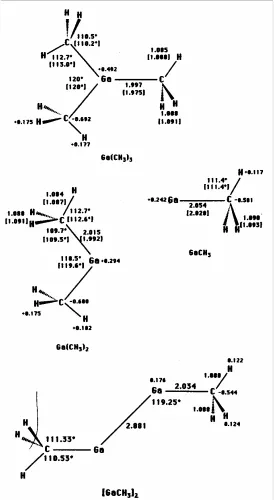
Figure 2.20. Geometries of Ga (CH3)3, Ga(CH3)2, and GaCH3. Distances are in angstrom, and angles in degrees. Therefore we can summarize the above steps into one overall reaction. ... 64
Figure 3.1. Temperature dependence of heater as a function of applied voltage. ... 68
Figure 3.2. Hg calibration spectra. References are in parenthesis. ... 73
Figure 3.3. Wavelength fit vs. pixel number. ... 74
Figure 3.4. Schematic drawing of metal alkyl bubbler... 75
Figure 3.5. Mode: control of growth run. ... 76
Figure 3.6. The decomposition rate of various alkyls as a function of temperature, measured by UV adsorption... 77
Figure 3.7. Degree of thermal decomposition of AsH3. ... 78
Figure 4.1. Dielectric function of a GaAs substrate at various temperatures from 100 to ... 83 Figure 4.2. Reaction verification of TMGa and TMSb. ... 85 Figure 4.3. Evolution of the imaginary part of the pseudodielectric function for GaSb
homoepitaxy on an initially degraded substrate under various combinations of precursor exposures... 88 Figure 4.4. Differences in 10 coefficient spectra with TMSb and TMG exposures: Sb -Sb for before TMG exposure and after recovery; Ga-Sb for the TMG-exposed surface and its condition before TMG exposure. ... 90 Figure 4.5. Dielectric function trend on GaSb substrate... 91 Figure 4.6. Spectral dependence of the recovery of a TMG-dosed (001) GaSb surface. TMG flow was initiated at 1930 s, and recovery started at 2000 s. Higher photon energies correspond to higher pixel numbers. Top: < r>. Bottom: < i>. ... 92 Figure 4.7. SEM image of the initial homoepitaxy sample. ... 93 Figure 4.8. AFM image of the initial homoepitaxy sample... 93 Figure 4.9. RDS spectra of a (100) GaAs surface in UHV (dashed curve) and in an
atmospheric-pressure OMCVD reactor (solid curve) (after ref. 1)... 95 Figure 4.10. α10 spectrum of a (2x4) reconstruction of (100) GaAs measured in our reactor.
... 95 Figure 4.11. Pseudodielectric function of a relatively thick GaSb layer grown
heteroepitaxially on GaAs... 97 Figure 4.12. Optical micrographs of the sample discussed in this section. (a) Image of
Figure 4.13 . SEM micrograph of a far-edge part of the deposited layer. ... 99
Figure 4.14. SEM micrograph of a central part of the substrate... 99
Figure 4.15. EDAX results for the central part of the sample. ... 101
Figure 4.16. The edge part of the wafer... 102
Figure 4.17. AFM images of the Fig. 4. 12 (2) region of the sample. ... 103
Figure 4.18. 3D dielectric function of GaSb homoepitaxy growth... 105
Figure 4.19. Effect of TMSb/TMG flow ratio on macroscopic roughness scattering as determined by LLS. ... 106
Figure 4.20. AFM images of the homoepitaxial GaSb material: (a) 2D, (b) 3D. ... 107
Figure 4.21. Normaski image of as-grown GaSb homoepitaxy... 108
Figure 4.22. SEM image of the homoepitaxial GaSb material... 108
Figure 4.23. TEM image of the interface of the homoepitaxial GaSb material... 109
Figure 4.24. Real part of <ε> for GaSb on GaAs. ... 110
Figure 4.25. Imaginary part of <ε> for GaSb on GaAs. ... 110
Figure 4.26. Trajectory of real vs. imaginary part of GaSb on GaAs at 4.0 eV. ... 111
Figure 4.27. Dielectric function of the GaSb layer grown heteroepitaxially on GaAs, compared to reference data on chemically stripped bulk GaSb... 112
Figure 4.28. AFM images of the GaSb layer grown heteroepitaxially on GaAs. (a): two-dimensional image; (b): three-two-dimensional image... 114
Figure 4.29. Nomarski image of GaSb grown heteroepitaxially on GaAs. ... 114
Figure 4.30. SEM cross-sectional image of the GaSb sample grown heteroepitaxially on GaAs. ... 115
Figure 4.32. XRD data for the final heteroepitaxial sample... 117 Figure 4.33. XRD data for the final homoepitaxial sample... 118 Figure 4.34. Powder diffraction file of GaSb. ... 118 Figure 4.35. Real-time < > spectra of the GaAs buffer layer with precursor flows as
indicated... 120 Figure 4.36. Dielectric function spectra of GaSb on GaAs at the beginning of heteroepitaxy.
The spectra are separated by 2 s intervals... 120 Figure 4.37. Curve fit... 122 Figure 4.38. Solutions of the three-phase model for the overlayer dielectric function εo for
different assumed values of the overlayer thickness d... 124 Figure 4.39. The trend of thickness, GaAs fraction, and void fraction in the interface for the initial stage of heteroepitaxy... 125 Figure 4.40. α10... 125
List of Tables
Table 2.1. Optical measurements... 7
Table 2.2. Optical constants of GaSb... 21
Table 2.3. Overview of epitaxial techniques. ... 31
Table 2.4. Lattice constant... 56
Table 2.5. Linear thermal expansion coefficient ... 57
Table 2.6. Bond length and linear thermal expansion coefficient of compounds... 57
Table 3.1. Impurity levels of various reactants... 67
Table 3.2. Growth conditions for GaSb homoepitaxy. ... 81
Chapter 1 Introduction
In most semiconductors bandgaps range from nearly zero (InSb) to about 6 eV (AlN). Photons that have sufficient energy can excite electrons from the filled valence bands to the empty conduction bands. If the photon energy is less than the electronic bandgap but well above any phonon energies, the absorption coefficient of the material is zero or very small.
Optical techniques, for instance, spectroscopic ellipsometry (SE) and reflectance-difference spectroscopy (RDS), are highly attractive for investigating surfaces and interfaces of samples in as-prepared conditions because optical probes are noninvasive, nondestructive, and can function in any transparent ambient [1]. As a result the use of ellipsometry in semiconductor processing has been extensive and continues to grow. However, this growth has been mainly in off-line measurements. Real-time diagnostics for monitoring and ideally controlling material processing, especially of thin film growth, have been a challenge of many researchers so far. Yet real-time monitoring and control of each step in growth processes has enormous potential to advance materials science through the optimization of new materials and, in microelectronic and optoelectronic technologies, through the optimization of new processes for device fabrication. Some results have already been reported. SE has been used to successfully demonstrate sample-driven closed-loop feedback control of epilayer composition [2-4] including graded compositions[5], thicknesses[6, 7], growth rates[8], and sample temperatures[7].
spectral information from 240 to 830 nm at the rate of 4 per second. This instrument has been used to demonstrate sample-driven closed-loop feedback control of the composition of InGaP layers deposited epitaxially on GaAs.
The antimonides are a highly promising and potentially important semiconductor material. Antimonides have the smallest bandgaps of the III-V semiconductors, with values ranging from the GaSb value of 1.6 µm (0.73 eV) to the 11 µm (0.11 eV) value for indium thallium antimonide. Therefore, optoelectronic devices fabricated from these materials can cover much of the infra-red wavelength range[9], which is particularly important for gas sensing at the ppb level[1].
GaSb-based devices in particular are promising candidates for a variety of military and civil applications that require wavelengths in the 2~14 µm range for photonic devices such as lasers, detectors, and photovoltaic cells. Recently, GaSb-based LEDs and lasers have been demonstrated [9]. With its 0.73 eV bandgap GaSb is often referred to as an intermediate-gap semiconductor. Its favorable combination of a bandgap energetically just below the 1.5 µm wavelength important for photonics and low effective mass (a consequence of its low bandgap), which translates into high electron and hole mobilities, make GaSb an ideal candidate for high-speed optoelectronic applications. In addition, its lattice constant matches solid solutions of various ternary and quaternary III-V compounds with bandgaps covering the wide spectral range of ~0.3 to 1.58 eV[10].
various growth temperatures, ranging from 550 to 570°C. The morphology of GaSb layers is extremely sensitive to the V/III ratio[12], as previously reported[13].
Among antimonides, GaSb is the most widely studied[14, 15]. It is known that Sb is non-volatile in contrast to P and As, which makes us to grow GaSb successfully.[9, 16-21] Thus the composition of epitaxially grown GaSb is in principle not self-regulating but can be affected by accumulated Ga or Sb resulting in nonstoichometry. Since the vapor pressure of Sb is much lower that of either or P, too high an Sb partial pressure may result in the formation of a second condensed phase, metallic Sb droplets on the surface. The group III metals are also not soluble in the semiconductor so any excess metal on the surface will also appear as second phase [22]. The presence of a second phase for Sb deposited on GaAs was recently demonstrated by Pitts et al. [23]using reflectance difference spectroscopy (RDS). On the other hand, if the V/III ratio is too low, then Ga droplets result [24]. Thus to grow stoichiometric GaSb by MBE the effusion rates of Ga and Sb must be controlled very carefully, nominally to parts in 104, and the same is expected for OMCVD. Haywood et al.
[25]reported good morphologies for substrate temperatures of 550 and 600°C with near-unity V/III ratios using TMGa and TMSb.
At present, GaSb technology is in its infancy and significant progress has to be made both in materials growth and processing aspects before it can be employed for device applications [26]. Pitts et al. [23] showed with reflectance difference spectroscopy (RDS) that the vapor pressure of Sb is very low so that Sb atoms remain on the GaAs surface.
requires knowledge about the chemical reactions between the substrate surface and the atoms or molecules such as TMGa and TMSb, which are used as precursors. In addition, we need to understand the processes taking place on the surface, for instance, diffusion, nucleation, adsorption and desorption. The overall OMCVD process is a complex interplay between fluid mechanics, heat and mass transport, and gas-phase and surface chemical reactions. Understanding, modeling, and controlling this interplay in typical OMCVD reactors is exceedingly difficult[27]. This means that despite its capabilities for epitaxial growth, OMCVD is not well understood. At least part of this lack of understanding has been the lack of any diagnostic tool that could obtain information in the OMCVD growth environment.
With respect to OMCVD mechanisms, Stringfellow[24],Moon [28], Aardvark et al[9], and Breiland et al [27] all provide good explanations, including brief looks at the origins of OMVPE and the early OMVPE history relative to compound semiconductors. Oleander [29] first suggests the use of rotating disks for better uniform deposition in chemical vapor deposition. Frolov et al [30] report in the OMCVD growth of GaAs using TMGa and AsH3
that rotation of the pedestal on which the substrate sits increases the growth rate. Since this would decrease the thickness of the mass transport boundary layer, this finding is also consistent with the hypothesis that the growth rate is limited by mass transport. Even though OMCVD is highly complex, it has emerged as a flexible and powerful synthesis technology for a wide range of epitaxial compound semiconductors.
system make it ideal for studying growth. The addition of a laser light scattering (LLS) capability has proven to be useful in that it allows macroscopic surface roughness to be detected, which is not possible with either SE or RDS.
Chapter 2 Background and Summary
The purpose of this chapter is to provide a context for the techniques used and data presented. We begin with a discussion of optical techniques for analyzing thin film growth in Sec. 2.1. Next, we describe the optical response of semiconductors, which includes an overview of the linear optical response and its relation to electronic band structure and sample properties. The optical response of structured materials is described in Sec.2.2, followed by an overview of SE and RDS. In Sec.2.4 we review OMCVD.
2.1 Optical techniques for analyzing thin film growths
For characterization of growing surfaces during OMCVD, optical techniques such as ellipsometry or RDS have found widespread use since electron-beam techniques such as reflection high-energy electron diffraction (RHEED) cannot be used in non-ultra high vacuum environments. Optical reflection techniques are one way that growth surfaces can be accessed, including the near-surface region of growing materials. Further details are introduced in the following.
2.1.1 Classification
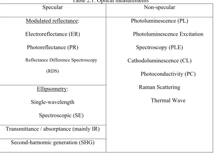
for the semiconductors that we are interested in here they are used mainly to assess material quality after growth and so are not of direct interest for real-time measurements.
Table 2.1. Optical measurements
Specular Non-specular Modulated reflectance:
Electroreflectance (ER) Photoreflectance (PR)
Reflectance Difference Spectroscopy
(RDS)
Ellipsometry: Single-wavelength
Spectroscopic (SE) Transmittance / absorptance (mainly IR)
Second-harnomic generation (SHG)
Photoluminescence (PL) Photoluminescence Excitation
Spectroscopy (PLE) Cathodoluminescence (CL)
Photoconductivity (PC) Raman Scattering
Thermal Wave
2.1.2 Ellipsometry
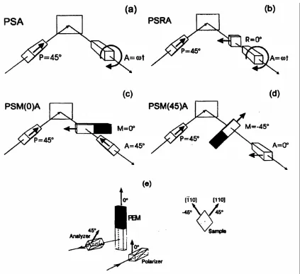
at oblique incidence from the surface under investigation. The reflected light is in general elliptically polarized. The shape and orientation of the ellipse depend on the angle of the incidence, the polarization state of the incident light, and the reflection properties of the sample. Fig. 2.1 [32] lists the most commonly used ellipsometric configurations.
Figure 2.1. An overview over the basic types of ellipsometric configurations: (a) fixed Polarizer-Sample-rotating Analyzer (b) fixed Polarizer-Sample-fixed retarder-rotating-Analyzer (c) fixed PEM(0)-fixed retarder-rotating-Analyzer (d) fixed Polarizer-Sample-PEM(45)
amplitude of the polarization within the plane of incidence (P) to the amplitude of the polarization perpendicular to the plane of incidence (S) is represented by tanΨ. The difference in the phase changes upon reflection is ∆. Ψ and ∆ essentially depend on the optical constants, n and k, of the layer materials and substrate, the physical thickness of the individual layers and the surface roughness. For a given material, the magnitude of the change in Ψ and ∆ is different at different angles of incidence. A larger change gives more accurate results, and for this reason data tend to be taken at or near Brewster’s angle, where the changes are largest.
Using the Jones matrix formalism, we can describe the operation of the ellipsometer in terms of the optical components and the Fresnel reflection coefficients rpand rs of the
sample. For the SE configuration shown in Fig. 2.2, which consists of a fixed polarizer, sample, rotating compensator (PSCA), and fixed analyzer we have
⎟⎟ ⎠ ⎞ ⎜⎜ ⎝ ⎛ ⎟⎟ ⎠ ⎞ ⎜⎜ ⎝ ⎛ ⎟⎟ ⎠ ⎞ ⎜⎜ ⎝ ⎛ − ⎟⎟ ⎠ ⎞ ⎜⎜ ⎝ ⎛ ⎟⎟ ⎠ ⎞ ⎜⎜ ⎝ ⎛ − − − − − ⎟⎟ ⎠ ⎞ ⎜⎜ ⎝ ⎛ ⎟⎟ ⎠ ⎞ ⎜⎜ ⎝ ⎛ − − − − − ⎟⎟ ⎠ ⎞ ⎜⎜ ⎝ ⎛ − ⎟⎟ ⎠ ⎞ ⎜⎜ ⎝ ⎛ = ⎟⎟ ⎠ ⎞ ⎜⎜ ⎝ ⎛ − y x s p i y x E E P P P P r r C t C t C t C t e C t C t C t C t A A A A E E 0 0 0 1 cos sin sin cos 0 0 ) cos( ) sin( ) sin( ) cos( 0 0 1 ) cos( ) sin( ) sin( ) cos( cos sin sin cos 0 0 0 1 ' ' ω ω ω ω ω ω ω ω δ (2.1)
where A and P define the analyzer and the polarizer angles, respectively, and C denotes the angle of the compensator fast axis measured with respect to the plane of incidence.
By multiplying the matrix out, evaluating the field at the detector, and taking the absolute square we obtain the transmitted intensity.
)} ( 4 sin ) ( 4 cos ) ( 2 sin ) ( 2 cos 1 {( )
(t I 2 t C 2 t C 4 t C 4 t C
I = dc +α ω − +β ω − +α ω − +β ω −
(2.2)
Figure 2.2. Schematic of the rotating-compensator multichannel spectroscopic ellipsometer
From the measured normalized coefficients we can derive ψ and ∆ as follows:
A
Q ⎟⎟−
⎠ ⎞ ⎜⎜ ⎝ ⎛ = − 4 4 1 tan 2 1 α
β (2.3)
⎥ ⎥ ⎥ ⎦ ⎤ ⎢ ⎢ ⎢ ⎣ ⎡ + = − A Q A sin 2 ) 2 tan( ) ( 2 cos tan 2 1 4 2 1 α δ α
χ (2.4)
Therefore, P Q Q P 2 cos 2 cos 2 cos 1 2 cos 2 cos 2 cos 2 cos χ χ ψ − −
= (2.5)
P P 2 sin 2 sin ) 1 2 cos 2 (cos 2 sin sin ψ ψ χ − =
∆ (2.6)
P P Q 2 sin 2 sin ) 2 cos 2 cos 1 ( 2 cos 2 cos cos ψ ψ χ − =
∆ (2.7)
Since sin∆ and cos∆ are measured simultaneously it is not necessary to consider whether the sign of ∆ is positive or not.
∆
=
= i
s p
r r
exp tanψ
ρ . (2.8)
For a bare substrate we can connect this to the dielectric function ε of the substrate using the Fresnel equations. We find
2 2
2 2
1 1 tan sin
sin ⎟⎟
⎠ ⎞ ⎜⎜ ⎝ ⎛
+ − +
= = = =
ρ ρ θ θ θ
ε ε ε ρ
a s
s p
r r
. (2.9)
ε is related to the complex refractive index by ε = (n + ik)2 where (n + ik) is the complex
index of refraction. If the sample is covered with one or more ovelayers we can still use Eq. (2.9), but in this case we get what is called the pseudodielectric function <ε>. The concept of <ε> is best reserved for cases where the overlayers are very thin, as for example natural oxides or microscopic roughness. If the layer thicknesses are comparable to the wavelength of light, the sample must be modeled with the Fresnel reflectance equations, with each layer represented by its own dielectric function and thickness.
With a good model, n, k and the physical properties of the material can be determined by matching the modeled Ψ and ∆ to the experimentally acquired Ψ and ∆ from the unknown sample. In this way the technique can be routinely used for determining the properties of compounds of unknown composition, as well as the thickness of the individual layers in multilayer stacks.
2.1.2.1 Spectroscopic sllipsometer
very good precision. This SE is an effective real time assessment technique.In SE the change in the polarization state of a beam of polarized light reflected from the sample being characterized is determined at many discrete wavelengths over a broad wavelength range, in our case from 1.5 to 6.0 eV. As with single-wavelength ellipsometry the change in the polarization state can be traced to the physical properties of the thin film by means of an optical model with the aid of regression analysis. SE has been used routinely for the characterization of already grown multilayer III-V compound semiconductor structures for many years.
SE instruments use a white light source, and individual wavelengths are selected for detection by either a motor-driven monochromator or a multichannel detector that can detect many wavelengths simultaneously. Increasing the number of angles of incidence and wavelengths at which data are acquired improves analysis precision, especially for complicated epitaxial structures. However the need to isolate the growth environment from the atmosphere requires the use of windows on the OMCVD growth chamber. Hence for the configuration used here we can obtain ellipsometric data only at a single angle of incidence.
2.1.2.2 Reflectance difference spectroscopy
Reflectance difference spectroscopy (RDS) is also an effective in situ technique of the
coverages of adsorbates[34]. Since the reflection probe senses optical anisotropy, RDS is also called reflectance anisotropy spectroscopy (RAS).
In isotropic materials like cubic semiconductors, the bulk is optically isotropic and hence the anisotropy arises entirely from the surface region. The surface anisotropy may arise from due to the different geometric ordering of atoms in two orthogonal directions parallel to the surface. The normalized reflectance-difference measurement is given by
y x
y x
r r
) r r ( r
r
+ − ≡ 2
∆ (2.10)
where rx and ry are the complex reflectance of light polarized linearly along the
indicated directions within the surface, for instance, for a (001) surface rx and ry become
> <110
r and r<110>. Normally, the order of magnitude of the signal is about 10-3, as indicated
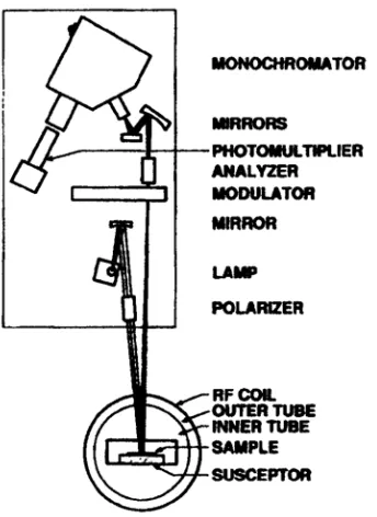
schematically below. Fig. 2.3 [35] shows a typical RD spectrometer used for crystal-growth measurements.
In our bench system the optical beam is not normal to the surface but enters at an angle of approximately 2°. Although a connection between normal-incidence spectra can be made, by analogy to the normal-incidence situation we provide the data in the form of the quantity actually measured, which for our system with a 5:1 ratio for the rotation rates of the sample and compensator is the 10th harmonic of the detected signal. Changes in this harmonic allow us to make inferences about the nature of the surface termination, which for III-V semiconductor growth surfaces usually consists of Group III or Group V dimmers.
In the ideal case the intensity reaching the photo diode array (PDA) from a rotating-compensator, rotating-sample spectroscopic polarimeter (RCSSP) synchronized at 5:1 ratio has the form
t sin b t cos a t sin b t cos a t sin b t cos a a
I = 0+ 2 ω + 2 2ω + 4 4ω + 4 ω + 10 10ω + 10 10ω (2.11)
where the normalized Fourier coefficients , , , a
a
4 2 0 2 2 β α
α = and β4 carry the information for calculating <ε > and α10 and β10 provide information about sample anisotropy, which is mainly due to surface dimers.
2.2 Optical response of semiconductors
dielectric response and the relationship between the dielectric function and electronic band structure of cubic materials, including the influence of sample properties, such as temperature, composition, and strain.
2.2.1 Dielectric function and polarization
2.2.1.1 Dielectric function
The dielectric function is the response of a material to an electromagnetic field. The dielectric function depends sensitively on the electronic band structure of a crystal, and investigations of the dielectric function by optical spectroscopy are very useful in understanding the overall band structure of a crystal.
The topic begins with Maxwell’s Equations, which describe propagation and also the boundary conditions for the electric and magnetic fields at each interface. In Gaussian units these equations are:
πρ 4 = ⋅
∇ DG (2.12)
0 = ⋅
∇ BG (2.13)
t B c 1 E
∂ ∂ − = × ∇
G G
(2.14)
t D c J c H
∂ ∂ + =
× ∇
G G
G 4π 1
(2.15)
where DG,BG,EG,ρ, and JG are the displacement field, magnetic induction, electric field,
magnetic field intensity, charge density, and current density, respectively. In optics, the charge density ρ and the current density JG are both zero so that above Maxwell’s equations
0 = ⋅
∇ DG (2.16)
0 = ⋅
∇ BG (2.17)
t D c 1 H ∂ ∂ = × ∇ G G (2.18)
and BG =µHG =HG since in optics the magnetic permeability µ = 1. Then (2.18) reads
t D c 1 B ∂ ∂ = × ∇ G G (2.19)
Now apply the curl to (2.14)
t ) B ( c 1 ) E ( ∂ × ∇ ∂ − = × ∇ × ∇ G G (2.20)
Using the identity, for instance
E ) E ( ) E
(∇× G =∇ ∇• G −∇2G
×
∇ (2.21)
and transforming the time derivative, we have
t ) B ( c E ) E ( ∂ × ∇ ∂ − = ∇ − • ∇ ∇ G G
G 2 1
(2.22)
Substituting from (2.19) for (∇×BG), we obtain
2 2 2 2 1 t D c E ∂ ∂ = ∇ G G (2.23)
By definition the dielectric function ε is
E
DG =εG (2.24)
0 2 2 2 2 = ∂ ∂ − ∇ t E c E G G ε (2.25)
And the solution to this wave equation has the form
t i r k i e E ) t , r (
E = •G−ω G
G G G
0 (2.26)
Therefore, Eq. (2.25)
0 2 2 2 2 = ∂ ∂ −
∇ )E
t c
( ε G (2.27)
) t , r ( E c e E t c t E c t i r k i G G G G G G 2 2 0 2 2 2 2 2 2 εω ε ε ω − = ∂ ∂ = ∂ ∂ • − (2.31)
Insert (2.30) and (2.31) into (2.25) Then,
0
2 2
2 − =
) t , r ( E ) c k
( εω G G (2.32)
Eq. (2.32) shows that the dispersion relation that relates k to ε and n.
0
2 2 2 − =
) c k
( εω (2.33)
2 2 2
ω
ε = k c (2.34)
By definition 2 2 2 2 ω c k
N = (2.35)
Then 2 1 2 2 2
2 ε ε ε
ω i
c k
N = = = + (2.36)
.
From Eq (2.36)
ik n ) ( N
N = ω = r + . nr is the ordinary index of refraction and k is the extinction
prepared to work in both representations. In essence, ε describes the material properties and
N optical propagation. We can also express as follow:
) (
nr 1
2 2 2 1
2
1 ε + ε + ε
= (2.37)
) (
k 1
2 2 2 1
2
1 ε +ε −ε
= (2.38)
or
2 2 1 =nr −k
ε (2.39)
k nr
2
2 =
ε (2.40)
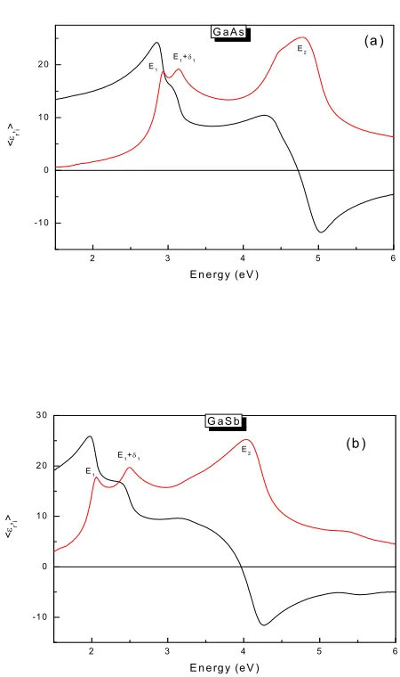
We use three different substrates in these measurements: (100)GaAs, (100)GaSb, and Ga. Fig. 2.4 shows reference pseudodielectric function data <ε> from 1.5 to 6.0 eV for these three substrates [37]. These data were obtained with the samples at room temperature. These dielectric functions show considerable structure in the form of peaks, which arise from transitions between the filled valence bands to the empty conduction bands in crystalline semiconductors at critical points in the joint density of states. The dielectric functions have the same basic features but differ in details. For example, both real and imaginary parts of the E1 and E2 peaks of GaSb are lower than those of GaAs. The main differences occur near the
energies of the critical-point transitions that give rise to the spectral features seen in the figure.
The real and imaginary parts of GaAs and GaSb of the dielectric function measured by ellipsometry are shown in Fig.2.4[37]. The values for refractive index nr, extinction
coefficient k, and reflectance R calculated from these data given Table 2.2 for various
wavelengths.
The dielectric function of the reference material, which means the curve can be identified by the decrease in peak energies with increasing temperature.
2 3 4 5 6
-1 0 0 1 0 2 0
<
εr
,i
>
E n e rg y (e V ) G a A s
(a )
E1
E1+δ1
E2
2 3 4 5 6
-1 0 0 1 0 2 0 3 0
<
εr
,i
>
E n e rg y (e V ) G a S b
(b )
E1
E1+δ1
E2
Table 2.2. Optical constants of GaSb.
eV ε1 ε2 n k R
1.5 19.135 3.023 4.388 0.344 0.398 2.5 13.367 19.705 4.312 2.285 0.484 3.5 7.852 19.267 3.785 2.545 0.485 4.5 -8.989 10.763 1.586 3.392 0.651 5.5 -5.527 6.410 1.212 2.645 0.592 6.0 -4.962 4.520 0.935 2.416 0.610
2.2.1.2 Relation to band structure
The dielectric function is closely related to energy band structure. As described in ref [36].
A typical example of a dielectric function relevant to the work done here is that of GaSb, which is shown in Fig. 2.5 [37], and its band structure Fig.2.6 [41]. The terminology used to describe the structures shown here is E1,E1+∆1, and E2, which occur near 2.0,2.5,
and 4.0 eV, respectively. This labeling convention was originally proposed by Cardona [42] according to the following:
1) Eoand E0+∆0(not shown here, but GaAs has) The ‘0’ subscript stands for the
center of the Brilliouin zone (Fig.2.8) and labels transitions along the <000> or Γ direction. For direct-gap zinc-blende semiconductors this is the energy at which ε2 becomes appreciable. ∆0 refers to the spin-orbit splitting at the zone center which is essential determined by the anion or Group V species.
2) E1and E1+∆1. The ‘1’ subscript refers to transitions occurring along the <111> or
3) E2. The ‘2’ subscript refers to transitions along the X direction. However, the E2
transition contains contributions from transitions occurring over a relatively large part of the Brillouin zone near the edges of the <100> and <110> directions. It has been shown that the height of the ε2 peak as measured by ellipsometry is very sensitive to overlayers on the surface, e.g., oxides or roughness, and can therefore be as a measure of surface quality[43].
The directions mentioned above follows Figs. 2. 7 (a) and (b). In Fig.2.7 (a) three important direction in k-space are inserted into the first Brillion zone of the bcc lattice. They are the [100] direction from the origin, Γ , to the H, the [110] direction from Γ or N, and the
[111] direction from Γ or P. These directions are commonly labeled by the ∆,Σ,and Λ,
2 3 4 5 6 -10
0 10 20 30
<ε
>
E (eV)
<ε1>
<ε2>
E1 E1+∆1
E2
Figure 2.5. Pseudodielectric function of crystalline GaSb.
2.3 Laminar Model
Optical modeling depends on relating measured quantities to sample properties by model calculations. Heteroepitaxial systems are by definition multilayer systems, so we consider here the description of the optical properties of two- and three-phase systems.
2.3.1 Two-phase model
We first consider the two-phase model (Fig. 2.8), which is the simplest reflecting system, consisting only of an optically thick bare substrate and transparent ambient with isotropic dielectric, respectively:
Figure 2.8. Two-phase model
Here, p and s are the directions parallel (p) and perpendicular (s) to the plane of incidence, εa, are the dielectric functions of the ambient and substrate, respectively, and εs θis the angle of incident.
The reflected field vectors, EGrpand EGrs, can be described in terms of the incident
⎟⎟ ⎠ ⎞ ⎜⎜ ⎝ ⎛ ⎟⎟ ⎠ ⎞ ⎜⎜ ⎝ ⎛ = ⎟⎟ ⎠ ⎞ ⎜⎜ ⎝ ⎛ is ip s p rs rp E E r r E
EGG GG
0 0
(2.41)
The Fresnel equations [44] for the complex reflectance at the ambient (a) and substrate (s) are given by
⊥ ⊥ ⊥ ⊥ + − = = s a a s s a a s ip rp sa p n n n n E E r ε ε ε ε (2.42) and ⊥ ⊥ ⊥ ⊥ + − = = s a s a is rs sa s n n n n E E
r (2.43)
where a corresponds to the ambient, in this case na = εa =1 and s to the substrate. The
corresponding indices of refraction for non-normal incidence nj⊥ are defined as
θ ε
ε sin2
a j j
n ⊥ = − . The elliptically measured complex reflectance ratio is defined as
s p
r r
=
ρ which can be inverted to give the dielectric function of the substrate as discussed
above. 2 2 2 2 1 1 tan sin sin ⎟⎟ ⎠ ⎞ ⎜⎜ ⎝ ⎛ + − + = ρ ρ θ θ θ ε ε a s (2.44)
2.3.2 Three-phase model, thin-film limit
We now consider the effect of an overlayer of thickness d . In this case two
interfaces must be considered and the resulting expressions will contain all the parameters of the system, the dielectric functions εs, and εo εa of the substrate, overlayer, and ambient, and the thickness of the film. For surface-physics work it is useful to consider first the situation where d/λ << 1, in which case we can do a small-term expansion and write to first order
θ ε ε ε ε ε ε ε ε ε ε λ π ε
ε 4 2
sin ) ( ) )( ( id a s a s o a o o s s
s − −
− −
+ >=
< (2.45)
where <ε> is the pseudodielectric function mentioned above. If εs >> εo >> εa =1 then Eq. (2.45) simplifies significantly to become
2 3 4 s s idε λ π ε ε >≅ +
< (2.46)
which is independent of εo. If εs = εs eiφ, then
) 2 2 3 (
4 φ π
φ ε
λ π ε
ε >≅ + +
< s i
i
s e
d
e (2.47)
The expressions for larger values of d are sufficiently complicated, especially when
absorbing materials are involved, that they are most easily evaluated numerically.
2.3.3 Effective medium theory
Using the definition, Eq (2.24) it follows that
b b a
a f
f ε ε
ε = + (2.48)
where fa and fb represent the volume fractions of regions a and b, respectively. Eq (2.48) is
the optical equivalent of capacitor in parallel. Eq (2.49) is the optical equivalent of capacitors in series.
The real purpose of effective medium theory is to take into account the effect of the screening charge that accumulates on boundaries between regions in a microscopically inhomogeneous medium. Since that is not practical, typical inhomogeneous systems are represented by “standard” effective medium expressions [45]. The generalized form can be written as
h b
h b b h a
h a a h h
f f
ε ε
ε ε ε
ε ε ε ε
ε ε ε
2 2
2 +
− +
+ − =
+ −
(2.50)
where εh is a “host” dielectric function, εa and εb are the dielectric functions of media “a” and “b”, and fa and fb are the relative volume fractions of a and b in the composite such that fa
+ fb = 1, and the 3 in the denominator is a screening factor appropriate to spherical inclusions.
2.4 Real-time diagnostics in OMCVD epitaxial growth
Real-time diagnostics refers to measurements with the sample in the setting in which growth is taking place, while it is taking place. After deposition samples can be characterized by many techniques, for example photoluminescence (PL), high-resolution crystal x-ray diffraction (HXRD), Hall mobility, C-V profiling, sheet resistivity, Scanning electron microscopy (SEM), transmission electron microscopy (TEM), optical transmission and reflectance, Raman scattering, and Fourier transform infrared spectroscopy (FTIRS) and ellipsometry. However, these provide information well after growth has taken place and do not provide a means for assessing mechanisms or for correcting growth processes if errors are occurring. Techniques for studying growth while it is occurring include RHEED, reflective optical probes including SE and RDS, and x-ray scattering, but all except optical probes are restricted to high or ultrahigh vacuum. As a result optical probes are becoming more sophisticated and have reached the point where they can control growth in real time. Aspnes [46] has provided an excellent review of this topic.
The relatively high pressure environment of OMCVD eliminates the use of electron-based in-situ techniques except when used with the help of an OMCVD-UHP transfer
growth surface for both incident and reflected beams. This means optical windows or ports that do not become coated during growth, although the technology of strain-free windows to provide this access is now well developed.
2.5 Epitaxial growth techniques
The term ‘epitaxy’ has come to mean the growth of one layer in a particular crystallographic orientation to the underlying, or substrate layer. The word , epitaxy’ comes from two ancient Greek words; epi (placed upon) and taxis (ordered), referring to the ordered single-crystal film formation on top of the underlying substrate crystal substrate.
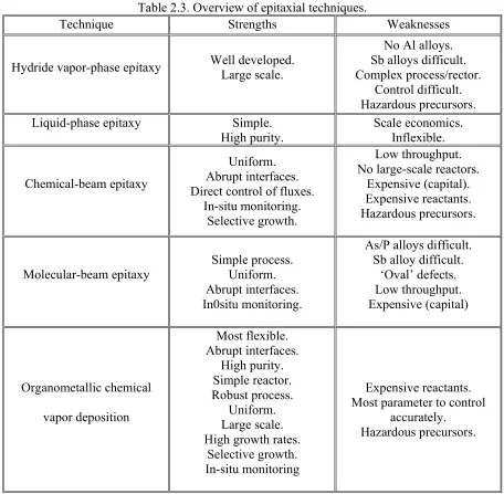
Vapor-phase epitaxial is a subject with considerable practical application, most obviously related to the production of semiconductor devices, but also to a whole range of other items. Many thin films are required to be single crystals with low defect density, and are produced via expitaxial growth processes.
Table 2.3. Overview of epitaxial techniques.
Technique Strengths Weaknesses
Hydride vapor-phase epitaxy Well developed. Large scale.
No Al alloys. Sb alloys difficult. Complex process/rector.
Control difficult. Hazardous precursors. Liquid-phase epitaxy Simple.
High purity.
Scale economics. Inflexible.
Chemical-beam epitaxy
Uniform. Abrupt interfaces. Direct control of fluxes.
In-situ monitoring. Selective growth.
Low throughput. No large-scale reactors.
Expensive (capital). Expensive reactants. Hazardous precursors.
Molecular-beam epitaxy
Simple process. Uniform. Abrupt interfaces. In0situ monitoring.
As/P alloys difficult. Sb alloy difficult.
‘Oval’ defects. Low throughput. Expensive (capital)
Organometallic chemical vapor deposition
Most flexible. Abrupt interfaces.
High purity. Simple reactor. Robust process.
Uniform. Large scale. High growth rates.
Selective growth. In-situ monitoring
Expensive reactants. Most parameter to control
accurately. Hazardous precursors.
Other epitaxial techniques such as liquid phase epitaxy (LPE), magnetron sputtering have also been developed for the epitaxial growth of III-V compound semiconductors, however all have limitations that restricted their use to simpler devices.
2.5.1 MBE
Molecular beam epitaxy was first developed by Arthur [50]and Cho [51] for the growth of III-V semiconductor epitaxial layers. In contrast with other techniques, MBE is elegantly simply in concept. In MBE, the basic elements - In, Ga, etc.- are evaporated from effusion cells as atomic or molecular beams onto a hot crystalline substrate. This necessarily occurs in UHV. The chambers are typically pumped by a combination of an ion pump, cryopump, diffusion pump, and/or turbomolecular pumps when high vapor pressures sources are being used. While MBE may be the ultimate research tool for the production of complex and varied structures, it has limitations for commercial application. Its primary advantage is the capability to access growing layers with UHV-compatible in situ characterization and
diagnostic tools such as LEED, RHEED, and mass spectrometry to provide information on crystal perfection during growth. These diagnostic tools can be used to control the growth process to define layer thickness down to a single molecular layer (ML) and composition.
The primary disadvantages of MBE are the requirement to periodically open the chamber to add source materials to the evaporation sources, nonuniform deposition, and the difficulty of growing materials with volatile species such as P. Not surprisingly, P- based compounds such as InP have not been extensively grown by MBE [52]. However, the valued cracker sources have recently been shown to remove the practical difficulty with growing phosphides by solid- source MBE, and to allow the growth phosphorus-containing heterostructures with excellent optical properties[53]. Substrate rotation is always used to minimize lateral variations in growth rate and composition.
tertramer As4 from elemental sources and as the dimer As2 from cracker cells. The two react
on the growth surface to form GaAs. The fact that MBE works at all is that As (and P) is highly volatile at growth temperatures and will be incorporated only if a crystallographic site is available. Thus growth always occurs with excess As (or P) being present, with stoichiometry automatically maintained and the growth rate determined by the arrival rate of the cation species to the growth surface. GaAsis unstable above a congruent evaporation temperature near 600°C.
The growth mechanisms of other compounds are similar to GaAs, with the exception of the antimonides owing to the fact that Sb is essentially nonvolatile. Consequently, the growth of antimonides by MBE is difficult, requiring constant monitoring of the arrival rates of the cationic and Sb species so that they remain in balance. This is one of the motivations for the present work.
2.5.2 OMCVD
surface-chemical reactions. Understanding, modeling, and controlling this interplay in the absence of real-time information is exceedingly difficult[28], which means that despite its capabilities OMCVD is still not well understood. The flow dynamics in typical OMCVD reactors is so complex that most of our understanding comes from complex computer simulations. Simplified principle of OMCVD of GaSb growth is illustrated in Fig. 2.9 [54, 55]; the precursors are carried to the GaAs or GaSb substrate by H2 carrier gas. After being
decomposed Ga and Sb get adsorbed on the surface of the substrate where they diffuse to their incorporation sites. Finally all other organics and unreactants are carried away to scrubber.
OMCVD systems consist of a gas handling system, a reaction chamber, scrubbers to remove toxic materials, and associated safety equipment. The gas handling system controls the incoming gases and directs them to the chamber using pressure regulators, mass flow controllers, pressure controllers, and valves. A carrier gas, usually H2 for semiconductor
materials, transports the reactants to the substrates and carries away the byproducts of the reaction.
The three primary mechanisms that govern OMVCD growth are thermodynamics, kinetics, and hydrodynamics. Since OMCVD basically an exothermic process, the maximum possible growth rate will be limited by thermodynamic forces trying to restore equilibrium, and will decrease as the temperature of the reaction site increases. If kinetics dominates the reaction rate will limit the growth rate and the growth rate will increase as the temperature increases. When the growth rate is governed by the mass transport of reactants to the substrate surface, the process is relatively temperature-independent.
There are two types of OMCVD reactors; horizontal and vertical configuration. The horizontal configuration is probably the most widely used for OMCVD growth. Drawbacks are nutrient depletion, transverse flow nonuniformity due to sidewalls, and sidewall deposits, which affect uniformity and surface quality and a have a tendency to create recirculation cells. However, most of these disadvantages have been solved by engineering or process optimization.
of rotation is to create a pumping action that pulls the gases down and across the substrates on the disk. Olander [29] first suggested the use of rotating disks to promote more uniform deposition in OMCVD. OMCVD preferentially operates under mass-transport-limited growth conditions, where the growth rate depends on the transport of the reactant gases to the surface and layer composition and uniformity can be controlled by the reactor geometry and flow conditions. Frolov et al [30] report in the OMCVD growth of GaAs using TMG and AsH3 that rotation of the pedestal on which the substrate sits increases the growth rate. Since
this would decrease the mass transport boundary layer thickness, this finding is also consistent with the hypothesis that the growth rate is limited by mass transport.
During OMCVD growth several types of reactions may take place. Reactions that occur entirely in the gas phase are termed homogeneous, and those that occur at a solid surface are heterogeneous. The processes in the gas phase are reasonably well understood. However, the processes on the growth surface are not. This situation is in contrast to molecular beam epitaxy (MBE), where considerable knowledge about growth processes has already been obtained. The optimum OMCVD performance depends on system elements such as the gas handling system that meters the incoming gases and directs them to the entrance of the reactor.
impeded the development of our understanding of OMCVD relative to that of MBE in this regard.
We comment finally on safety issues. MBE is a relatively safe growth process since everything is contained within a stainless steel shell except when the chamber is opened as for example replenishing effusion cells. On the other hand, OMCVD uses precursor species such as AsH3, which are extremely toxic and must be handled with great care. This requires
OMCVD growth systems to be monitored constantly by toxic gas monitors, and personnel who work with OMCVD growth to be fully trained in the handling of toxic materials, the use of self-contained breathing apparatus (SCBA) gear, and how to respond in emergency situations. These safety procedures add considerably to the cost of OMCVD setups, but in industrial situations this added cost is usually counterbalanced by increased production rates and by avoiding the need to open up the reaction chamber on occasion to replenish the reaction species.
2.6 Crystal structure and defects
2.6.1 Crystal structure
III III
[010]
V
[001]
[010]
Figure 2.10. Two possible orientations of the zinc-blende crystal structure common to many of the III-V compound semiconductors such as GaAs, GaSb, and GaP.
parallelepipeds, of the cubic zincblende structure is same as that of diamond except that the two sublattices are occupied by different atoms. One lattice is composed of group III, and the other of group elements. The crystal is uniquely identified by description of the atomic arrangement within a layer and the placement of consecutive layers relative to each other.
2.6.2 General crystal defects
Single-crystal thin films are of technological importance in modern electro-optics and electronics because they are the real estate upon which everything is built. A successful thin-film technology may rapidly develop new electronic and electro-optic devices by bypassing the more expensive approach of bulk crystal development. However, to ensure that the resulting devices perform efficiently, the films must be as defect-free as possible.
as-grown GaSb is generally p-type owing to the incorporation of large quantities of Ga on Sb sites, where it acts as an acceptor.
The simplest point defect is a lattice vacancy, which is a missing atom or ion in the crystal structure of an elemental crystal, also known as s Schottky defect. If the absence of an
atom on a lattice site causes no changes in the rest of the crystal, we can apply in a simple way the principles to the case of vacancies in elemental crystals. The crystal will consist of N atoms and n vacant lattice sites (vacancies). The probability of finding an unoccupied state – assuming that the energy to create such a vacancy is given by Ev (eV) - is related to the
energy required to produce the vacancy and the temperature of the crystal. This probability that a given site is vacant is proportional to the Boltzmann factor ( kB ) for thermal
equilibrium.
) /
exp( 1
) /
exp(
T k E
T k E n
N n P
B v
B v
v + −
− =
+
= (2.47)
where N is the number of atoms and n is the equilibrium number of vacancies. If n << N, then
) exp(
T k
E N
n
B v
−
= (2.48)
Eq. (2.48) shows that at temperatures above absolute zero, elemental crystals at equilibrium contain vacancies. The equilibrium concentration of vacancies decreases as the temperature decreases.
Figure 2.11. Examples of point defects.
The other major defect that occurs in epitaxially grown material is the line imperfection known as a dislocation or linear lattice defect. These are the major way by which stress caused by lattice mismatch is released. Dislocations come in several basic types. We first describe an edge dislocation.
Figure 2.12. Illustration of edge and screw dislocations. (a) Model of a simple cubic lattice; the atoms are represented by filled circles, and the bonds between atoms by springs, only a few of which are shown; (b) positive edge dislocation DC formed by inserting an extra half-plane of atoms in ABCD; (c) left-handed screw dislocation DC formed by displacing the faces ABCD relative to each other in direction B; (d) spiral of atoms adjacent to the line DC in (c).
The mechanism responsible for the mobility of a dislocation is shown in Fig. 2.13 [57]. Two neighboring atoms (1 and 3) on sites adjacent across the slip plane are displaced relative to each other by the Burgers vector when the dislocation glides past. The movement of one dislocation across the slip plane to the surface of the crystal produces a surface slip step equal to the Burgers vector. If atoms on one side of the slip plane are moved with respect to those on the other side, atoms at the slip plane will experience repulsive forces from some neighbors and attractive forces from others across the slip plane.
which displaces the planes on either side. In figure 2.12 (c) the crystal on the side of ABCD has been displaced relative to the crystal on the other side, with the displacement in the direction of the line AB. Imagine taking the line AD and rotating it anticlockwise with DC
as the axis of rotation. After 360o rotation it has moved down one lattice position in an unbroken plane. The set of parallel planes initially perpendicular to DC have been
transformed into a single surface, and the spiral nature is clearly demonstrated by the atom positions.
Figure 2.13. Movement of an edge dislocation: the arrows indicate the applied shear stress tending to move the upper surface of the specimen to the right.
ThisDC is a screw dislocation transforms successive atom planes into the surface of
Ichimura et al.[59] carried out a thermodynamic calculation of native defect concentrations in AlxGa1-xSb alloys. The theoretical model they used is extended from that of
Van Vechten [60]. The enthalpies of vacancy of formations used here were calculated by Van Vechten on the basis of his macroscopic cavity model. In his model, the formation enthalpy of a vacancy is mainly the surface energy of a cavity. The formation enthalpy of VSb
is larger than that of VGa because the covalent radius of Sb is larger than those of Ga [59].
The results of these theoretical calculations which give the concentration of each of the native defects like VGa, VSb, GaSb and SbGa for crystals grown from Ga and Sb melts as a
function of temperature are shown in Figs.2.14 and 2.15.
Figure 2.15. Temperature dependence of antisite concentration in GaSb.2.7 Thin Film Growth
Thin films are deposited on substrates to achieve properties obtainable or not easily obtainable in the substrates alone. Additional functionality in thin film growth can be achieved by depositing multiple layers of different materials. This section handles fundamentals for thin film growth.
2.6.3 Growth modes
Frank-Van der Merwe growth is the most desirable and is most used in device production. This is the usual growth mode for lattice-matched materials with high interfacial bond energies. It occurs when cohesive energy between the film and substrate atoms is greater than the cohesive energy of the film, but monotonically decreases as each new film layer is added. In Frank-van der Merwe growth atoms more strongly bound to substrate than to each other. As a result the atoms first aggregate to form monolayer islands which then expand and coalesce to form the first monolayer. 2D growth can be enhanced if the islands in the first incomplete layer are small because an atom on top of a smaller island will visit the island edges more frequently, thereby increasing its chance to hop down and form part of the growing crystal.
Volmer-Webber (island) growth results in the formation and growth of isolated islands. This phenomenon occurs when the cohesive energy of the film atoms is greater than the cohesive binding between the film and substrate atoms. In this mode, deposited atoms are more strongly attracted (bond) to each other than to the substrate. Thus they will first aggregate to form islands and as deposition continues theses islands will grow and finally form a continuous film. For highly mismatched combinations of semiconductor materials, the layer grown often crystallizes in the Volmer-Weber growth mode, which means that islands or clusters are formed on an unwetted substrate surface. Island diffusion can proceed by many different mechanisms, but smaller islands diffuse faster than large islands.
the monotonic decrease in binding energy with each successive layer is energetically overridden by some factor such as strain energy due to lattice mismatch and island formation becomes more favorable. That is to say, the formation of Stranski-Krastanow islands is closely related to an epitaxial misfit and the accumulation of elastic strain energy in the epilayer. Strain relaxation occurs through the rearrangement of the deposited material when 3D islands are formed. The formation of 3D islands the strain situation completely. In this mode, the stress caused by the mismatch of the lattices of the film and the substrate produces a thermodynamic driving force that modifies structure and morphology. Deposition begins with complete wetting of the substrate. The continuous thin film is often referred to as the wetting layer. The total energy of the system decreases until the substrate is covered by one monolayer of deposit. This wetting is due to the energy contribution from the substrate/epilayer interface. The formation of islands changes the strain distribution in the wetting layer. The strain relaxation in the islands brings an energy minimum on the surface of the dot. This minimum energy is the driving force for the growth of the islands. The maximum energy around the edge of the island is due to the high compressive strain in this region. It was traditionally believed that an array of 3D islands is always unstable and that large islands will grow at the expense of evaporation or dissolving of small islands. This process is known as Ostwald ripening [62].
also favors layer-by-layer growth. If the deposited layer is slightly mismatched to the substrate the deposited film will be strained so that its in-plane lattice constant fits the lattice constant of the substrate. Here, let us assume that the lattice mismatch between the epitaxial layer thin film and the substrate is not too large, say only around 1% of their lattice constants. To minimize this small mismatch between the two kinds of atoms, the thin film will develop a kind of lattice defect known as a dislocation (see also section 2.6.2). For example, if the lattice constant of the thin film is smaller than the substrate then the mismatch can be compensated by periodically inserting an extra plane of atoms again. This kind of dislocation is known as a misfit dislocation.
2.6.4 Kinetics
It is well known that reactor parameter settings such as the growth pressure, bubbler pressures, growth temperature, bubbler temperatures, mass flow controller and pressure controller in the precursors and carrier gas, and so on, affect critically to the growth.
For the gas-phase epitaxy, the film growth kinetics is largely determined by a few categories of atomistic rate processes, which form the basis also for all more complex growth situations. Here, real-time diagnostics will help to analyze and understand the basic mechanism of epitaxial growth and help for technological growth control as well.
In OMCVD the rate of decomposition of precursor molecules influences the overall rate of film growth. Because the precursor decomposition rate depends strongly on the growth temperature, and the deposition rates are no longer independent, and the flux and diffusion rates cannot be independently controlled.
The concept of a boundary layer is useful in understanding the gas flow kinetics. The velocity of a fluid at the substrate or a constraining wall must be zero, while in the bulk of the fluid it is some uniform value. The region in which the velocity is changing because of the presence of the wall or the substrate is called the boundary layer. At the gas velocity increases, this layer becomes thinner. Ideally the bulk flow should be smooth or laminar, but practically, changes in the cross-sectional area, density gradients, turbulence, and temperature gradients can all cause recirculation cells to occur.
In our system we can assume that the fluid flowing into the reactor is mostly H2 with
substrate is being rotated the velocity changes over the radius. The natural velocity of the substrate, which depends on the viscosity and density of carrier gas and the substrate spin rate ω, is in rad/s:
) ( 8838 .
0 mk
v= ω (2.49)
where the kinematic viscosty,mk,which is equal to , ( )( )
ref ref ref k
T T p p
m , mk,ref is 1.09 cm
2/s. We
can guess how much the total flow rate (Q: in sccm), mostly hydrogen, needs to be allowed
to flow[30]. We can relate this ν to the volume flow rate, Q.
) 15 . 273 )( 760 (
60 2
T Torr p r
v
Q= ⋅ ⋅π⋅ (2.50)
Adsorption and arrival rate of atoms at a surface(R) and boundary layer thickness:
We can assume that the growth rate is limited by the rate of arrival of film precursors to the surface .The gaseous precursors are also assumed to immediately decomposed upon contact with the hot substrate surface. This is a reasonable assumption for high temperatures and agrees well with reports.
Supposing that atoms strike a solid surface exposed to a monoatomic gas at temperature T and pressure P. It is important to determine the arrival rate of the atoms µ