ISSN(Online): 2320-9801
ISSN (Print): 2320-9798
I
nternational
J
ournal of
I
nnovative
R
esearch in
C
omputer
and
C
ommunication
E
ngineering
(A High Impact Factor, Monthly, Peer Reviewed Journal) Website: www.ijircce.com
Vol. 7, Issue 5, May 2019
Low-Power and Area-Efficient Shift
Register Using Pulsed Latches
Jacob B Cacko, Gajendra Sujediya
Assistant Professor, RIET Jaipur, Rajasthna, India
Research Scholar, RIET Jaipur , Rajasthna, India
AB STRACT: Th is paper pr oposes a low-p ower an d ar ea-effici en t sh ift r egister usin g pulsed latch es. Th e ar ea an d power con sumption ar e r educed by r eplacin g flip -flops with pulsed latch es. Th is meth od solves th e timin g pr oblem bet ween pulsed latch es thr ough th e use of multiple n on -over lap dela yed pulsed cl ock sign als in stead of th e con ven tional sin gle pulsed clock sign al. Th e shift r egister uses a small n umber of th e pulsed clock sign als by gr oupin g th e latch es to sever al sub sh ifter r egister s an d using addit ional tempor ar y st or age latch es. A 256- bit sh ift r egister usin g pulsed latch es was fa br icated usin g a 0.18 $mu{rm m}$ CMOS pr ocess with ${r m V}_{r m DD}=1.8{rm V}$. Th e cor e ar ea is $6600 mu{r m m}^{2}$. Th e power con sumption is 1.2 mW at a 100 MHz clock fr equ en cy. Th e pr oposed sh ift r egister saves 37% ar ea an d 44% power compar ed to th e con ven tion al shift r egister with flip-flops.
I. INTRODUCTION
The clock network is one of the large consumers of dynamic power. Therefore, reducing power in the clock network can impact the overall dynamic power significantly. Designers already use a variety of techniques to reduce the clock power using smaller clock buffers, reducing the overall wiring capacitance, employing clock gating to reduce the dynamic power, and de- cloning to move the clock buffers at higher levels of hierarchy . Even with these techniques, the dynamic power of clock network can be large since registers are used as state elements in the design. In general, a flip - flop is used as the register or you can say sequential circuits. For mobile devices, where power consumption is the prime concern with high speed of operation, there is requirement of low power flip- flops in designs. Many other applications where shift registers are commonly utilized such as digital filters ,communication receivers and image processing IC’s. In particular, edge- triggered sequential circuits
PULSED LATCH TECHNIQUE
Flip - flop is the most common form of sequencing elements. Flip - flop synchronization with the clock edge is widely used because it is matched with static timing analysis, however, high sequencing leads to overhead in terms of delay, power and area. A latch is quite simple and at the same time consumes much less power than that of the flip- flop. However, it is little difficult to apply static timing analysis with latch design because of the data transparent behavior. A latch is capable of capturing data during the time duration determined by the width of clock waveform. This time duration is known to be very sensitive to its operation.
ISSN(Online): 2320-9801
ISSN (Print): 2320-9798
I
nternational
J
ournal of
I
nnovative
R
esearch in
C
omputer
and
C
ommunication
E
ngineering
(A High Impact Factor, Monthly, Peer Reviewed Journal) Website: www.ijircce.com
Vol. 7, Issue 5, May 2019
The first component is the energy dissipated when the flip-flop is clocked while the data of the flip-flop is unchanged. The second component is the additional energy required to write a different data value into the flip-flop. In a typical flip-flop, the two energy components are comparable. However, in most systems, the data rate of a flip-flop is typically much lower than its clock rate. This means that identical data value is being loaded with very high probability. Thus, the power saving techniques for flip-flops mostly concentrates on the clock energy reduction.
Many different circuit techniques for latches and flip-flops have been explored for various needs. The low power requirement merely adds another factor to the trade-off during the design process. Referring to the power equation
P = CV2f
Where C= capacitance
V=Voltage
f=Frequency
The techniques for low power flip-flops are obvious. We will not discuss voltage reduction techniques because they are fairly straightforward when applied to flip-flop circuits. Some techniques attempt to reduce the gate capacitance connected to the clock signal. Others attempt to reduce or increase the transistor count to reduce power by minimizing unnecessary internal node switching. Various implementations of CMOS latches were introduced. Each circuit provides a different trade-off among setup time, hold time, data-to-output and clock-to-output delay. The use of NMOS pass transistors instead of transmission gates reduces the loading capacitance of the clock pin at the cost of reduced speed. This eliminates the need for a two-phase non-overlapping clock on the system or a phase splitter inverter that consumes power inside the cell. When logic 1 is propagated through the NMOS pass transistor, threshold voltage loss occurs in circuit.
Reduced Swing Clock
Referring to the golden power equation, the most attractive parameter to attack is the voltage swing V due to the quadratic effect. Generally, it is difficult to reduce the load capacitance or frequency of clock signals due to the obvious performance reasons. We will discuss some power reduction techniques for clock signals based on voltage swing reduction.
One such idea proposes to reduce the clock swing by half. Notice that in CMOS design, a clock signal is only connected to the gate of a transistor when it reaches a sequential element. The clock signal is seldom connected to the source or drain of a transistor. Inside a sequential cell, the clock signal is used to turn on or turn off transistors.
Consider a 5V digital CMOS chip with an N-transistor threshold voltage of O.8V. For a 5V regular full swing clock signal, an N-transistor gated by the clock will turn on if the clock signal is above O.8Y. Therefore if we limit the swing of the N-transistor clock signal from zero to 2.5V (half swing), the on-off characteristics of all N transistors remain digitally identical. Similar
Exchange of flip-flop with proposed pulsed latch
ISSN(Online): 2320-9801
ISSN (Print): 2320-9798
I
nternational
J
ournal of
I
nnovative
R
esearch in
C
omputer
and
C
ommunication
E
ngineering
(A High Impact Factor, Monthly, Peer Reviewed Journal) Website: www.ijircce.com
Vol. 7, Issue 5, May 2019
II. PULSED LATCH ISSUES AND OPTIMIZATION
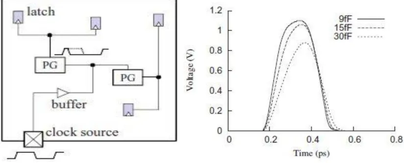
If pulse generators and pulsed latches are not placed properly, timing violations might occur. A pulse generator generates a brief clock signal to each connected latch, after receiving the clock waveform from the clock source. Latches can share the same generator with the same pulse width. A pulse generator is a combinational circuit itself. The output load capacitance would also affect the delay and driving capability of a pulse generator [8]. If a pulse generator and latches are not placed properly, the wire length might become too long and thus make the generated pulse width distorted causing serious timing violations. In Figure 4.1, load capacitance and the pulse width are inversely proportional to each other. Therefore, after circuit placement, the pulse-width degradation might cause timing constraint violations, e.g., setup/hold time violations. A multilevel pulsed latch prevents pulse width degradation.
Fig. 1 Multilevel PL & Pulse width distorts as CL increases
III. PROPOSED APPLICATIONS OF PULSED LATCH
There are wide range of applications for pulsed latches. Pulsed latches could be used in portable devices where low power consumptions is necessary like the applications where flip-flops could be replaced with pulse latches i.e. in pipelining or as sequencing element or as register.
Johnson Counter using pulsed latch
ISSN(Online): 2320-9801
ISSN (Print): 2320-9798
I
nternational
J
ournal of
I
nnovative
R
esearch in
C
omputer
and
C
ommunication
E
ngineering
(A High Impact Factor, Monthly, Peer Reviewed Journal) Website: www.ijircce.com
Vol. 7, Issue 5, May 2019
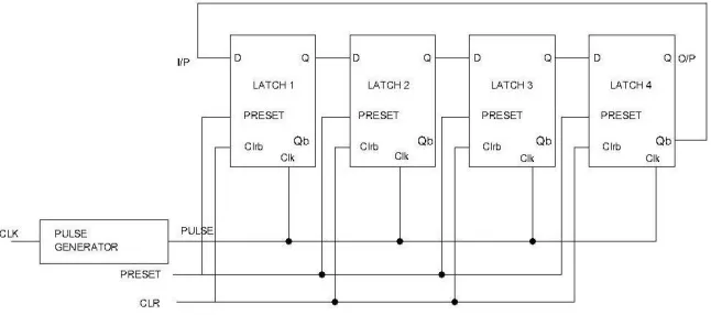
Fig. 2 Johnson counter using pulsed latch
IV. SIMULATION RESULTS
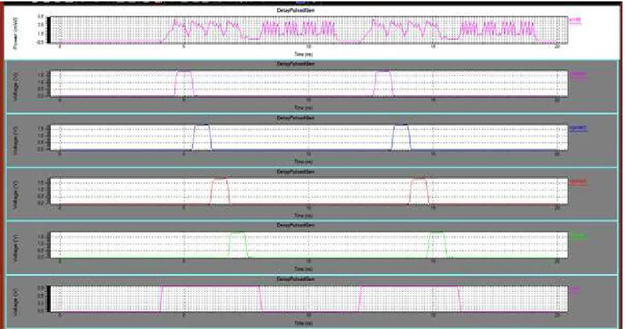
Simulations of all the circuits were performed in Tanner tools v14.1 using 180 nm technologies. Figure 6.1 to figure 6.12 shows the schematic and waveform of proposed circuits implemented in the tool. The waveform depicts the working of application using pulsed latch. Results of simulation are listed from table 6.2 to table 6.7. Table 6.1 provides the performance comparison between the D flip-flop and pulsed latch. Table 6.2 to 6.7 provides the comparative study of different applications using pulsed latch and different application using conventional D flip-flop i.e. SISO, SIPO, PISO, PIPO, Ring counter, Johnson counter respectively.
ISSN(Online): 2320-9801
ISSN (Print): 2320-9798
I
nternational
J
ournal of
I
nnovative
R
esearch in
C
omputer
and
C
ommunication
E
ngineering
(A High Impact Factor, Monthly, Peer Reviewed Journal) Website: www.ijircce.com
Vol. 7, Issue 5, May 2019
Fig. 4 Delayed pulse clock generator output waveform
Johnson counter using pulse latch
The Johnson counter is an alteration of Ring counter. In Johnson counter, the inverted output of the last stage flip-flop is feedback as the input of first flip-flop. If we use n flip-flops to design the Johnson counter, it is known as 2n bit Johnson counter or Mod 2n Johnson counter.
Johnson counter requires only half number of flip-flops as compared to a Ring counter to design the same Mod counter. It is also an important advantage of it.
ISSN(Online): 2320-9801
ISSN (Print): 2320-9798
I
nternational
J
ournal of
I
nnovative
R
esearch in
C
omputer
and
C
ommunication
E
ngineering
(A High Impact Factor, Monthly, Peer Reviewed Journal) Website: www.ijircce.com
Vol. 7, Issue 5, May 2019
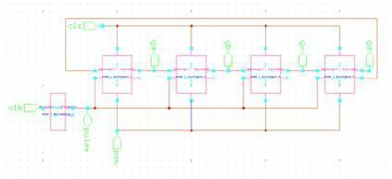
Fig. 5 Johnson counter using pulsed latch
V. CONCLUSIONS
The requirement of replacement element for flip-flops in recent trend, led to migration from flip-flops to the pulsed latch for low power consumption, less area and delay applications. In this thesis, we have proposed different applications of pulsed latch using 180nm technology in Tanner tool v 14.1 and performance is compared with application using flip-flop. The number of transistors utilized in pulsed latch is less than that of flip-flop, hence area is significantly reduced. Pulsed latch circuit saves power consumption and power delay product in comparison with flop circuit hence it can be inferred from the results that the circuits using the pulsed latches can be used instead of flip-flop for low power, less area and high speed applications. It also eliminates one latch per cycle and doesn’t require clock complement. Other advantages include minimised sequencing overhead, easier timing verification, lower delay and time borrowing capability. The trading towards applications using pulsed latches from conventional flip-flop circuits in heavy pipelining, mobile devices or in low power ASIC circuits is immense achievement in field of VLSI designin
REFERENCES
[1] S. Shibatani, A. H. C. li, “Pulse latch approach reduce dynamic power”, EE times online, 2016.
[2] P. Reyes, P. Reviriego, J. A. Maestro, and O. Ruano, “New protection techniques against SEUs for moving average filters in a radiation
environment,” IEEE Transactions NuclearScience, vol. 54, no. 4, pp. 957–964, Aug. 2017.
[3] M. Hatamian et al., “Design considerations for gigabit Ethernet 1000 base-T twisted pair transceivers,” Proc. IEEE Custom Integration Circuits
Conference, pp. 335–342, May 1998.
[4] H. Yamasaki and T. Shibata, “A real-time image-feature-extraction and vector-generation vlsi employing arrayed-shift-register architecture,”
IEEE Solid-State Circuits, vol. 42, no. 9, pp. 2046–2053, Sep. 2017.