A 4.7 nA, 1.2V, CMOS Current Reference
Circuits Using Sub-threshold Operation
Rakesh Vaghela 1, D.S.Ajnar 2, P.K.Jain 3
P.G. Student (Microelectronics and VLSI Design), Department of E&I, Shri G. S. Institute of Technology and Science,
Indore, M.P, India 1
Associate Professor (Microelectronics and VLSI Design), Department of E&I, Shri G. S. Institute of Technology and
Science, Indore, M.P, India 2
Associate Professor (Microelectronics and VLSI Design), Department of E&I, Shri G. S. Institute of Technology and
Science, Indore, M.P, India3
ABSTRACT: A low-power CMOS current reference circuit operating with a supply voltage ranging from 1.2V to 1.8V has been implemented in 0.18 UMC CMOS process, providing a mean reference current of 4.7nA.The device consists of MOSFET circuits operated in the saturation and threshold region and uses no resistors. Accurate sub-threshold design allows the circuit to work at room temperature with supply voltage 1.2V . The average temperature coefficient measured from -400C to 800C is 854ppm/0C and the line regulation is 0.9%/V.
KEYWORDS: complementary metal-oxide semiconductor (CMOS), current reference, power-aware large-scale integrations(LSIs),self-biasing circuit,subthreshold region, temperature dependence, ultralow power,weak inversion..
I. INTRODUCTION
Current reference circuits are important building blocks for analog and mixed-signal circuit systems in micro-electronics. they are indispensible components for producing reference current for various analog circuits, such as operational amplifiers,analog buffers,oscillators,and analog-to-digital/digital-to-analog converters. Nano ampere current reference have been strongly desired particularly for use in ultralow-power large-scale integration(LSI) applications. such as radio frequency identifications(RFIDs),implantable medical devices, and smart sensor networks.these LSIs have to operate with ultralow power ,e.g.,a few microwatts or less, because they will probably be placed under conditions where they will rely on poor energy sources, such as microbatteries and energy-harvesting devices.because the power dissipation and performance of these circuits are determined mainly by their bias currents,current reference with nanoampere-order currents are required to ensure stable and highly precise circuit operation
II. RELATEDWORK
Reference [1] shows a current reference circuit with a 1.4µW 24.9ppm/0C current reference with process insensitive temperature compensation in 0.18µm CMOS.The proposed circuit employs ratio between the process independent temperature coefficients of resistor and and comensation voltage.it consumes 1.4µW from 1-v supply.it acchives temperature coefficient of 24.9 ppm/0C with 00C to 1000C. Reference [2] is A Resistor-free Temperature Compensated CMOS current reference The proposed circuit is implemented 0.18µm CMOS standard technology and operates with supply voltage in the range of 2V to 2.8V from -250/C to 1300/C.the reference current is 1µA ± 1nA has a temperature coefficient of 12.9 ppm/0C and a line sensitivity of 8.7 nA/V.. Reference [3] is A 2.6nW,0.45V Temperature Compensated Subthreshold CMOS Voltage reference circuit shows a voltage reference circuit operating with all transistor biased in weak inversion providing a mean reference voltage of 257.5 mV has been fabricated in 0.18µm CMOS standard technology.accurate subthreshold design allows subthrshold design allow the circuit to work at room temperature with supply voltage down to 0.45V.and an average current consumption 5.8 nA and an average temperature coefficient of 165 ppm/0C with a standard deviation of 1000C in a temperature range from 00C to 1250C. Reference [4] is A CMOS Sub 1-V nano power current and voltage reference with leakage compensation.in this paper a CMOS Sub-1-V nanopower reference is proposed which is implemented without resistors and only CMOS transistors.the proposed circuit has most attractive merit that it can afford reference current and voltage simultaneously. moreover the leakage compensation technique is utilized, and thus it has a very low temperature for wide temperature range.the proposed circuit is verified by SPICE simulation with a 0.18µm CMOS standard technology. The temperature coefficient of reference voltage and reference current are 0.0037%/0C AND 0.0091%/0C, respectively also the power supply voltage can be as low as 0.85V and its power consumption is only5.1 nW.
III.CIRCUITDESIGN
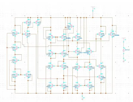
Fig.1 shows our current reference circuit .the circuit consists of a bias-voltage subcircuit is a modified â multiplier self biasing circuit that uses a MOS resistor M3,instead of ordinary resistors. Bias voltage VB for mos resistor M3 is
generated by a diode-connected transistors M4.the current-source subcircuit accepts bias voltage VB and generates
reference current IOUT that is independent of temperature and supply voltage .All MOSFET are operated in the
subthreshold region, except for M3 and M4.A start-up cicuit is required to avoid the stable state in the zero bias condition
.
The bias-voltage subcircuit is divided into three components.thsese components as follows: 1) â multiplier self-biasing circuit with MOS resistor.
2) diode-connected transistor(M4)
3) p-channel operate MOS current mirror
The subthreshold drain current ID of a MOSFET is an exponential function of the gate-source voltage VGS and the
drain-source voltage VDS ,and is given by
Where K is the aspect ratio (W/L) of the transistor,µ is the carrier mobility, Cox is the gate-oxide capacitance, VT (= kB T/q) is the thermal voltage, KB is the Boltzmann constant, T is the Temperature, q is the elementary
charge,VTH is the threshold voltage of a MOSFET,and η is the subthreshold slope factor.for VDS >0.1 V,current ID is
Fig. 1. Circuit Diagram of Proposed Current Reference circuit.
IV.EXPERIMENTAL RESULTS
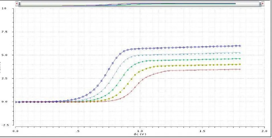
Fig2.Simultaed output current Iref at room temperature as function of suplly voltage
Fig 2 shows the supply voltage dependence of the output reference current Iref at room temperature.The power supply voltage was set in the range of 1.2V to 1.8V.the output current was about 4.75 nA and almost constant at room temperature in the range of -400C TO 800C.the temperature coefficient is 854ppm/0C respectively.almost a consatant reference current was obtained over a wide temperature range.
Fig 3.shows the measured output current at different temperature range from -400C to +800C. The power supply voltage was set in the range of 1.2V to 1.8V.when VDS>0.1 current Iref is almost independent of VDS and is given by
Fig 4.measured output current Iref at different temperature.
Fig 4.shows measured output current as a function of temperature.range from -400C to 800C with a temperature
coefficient of 854PPM/0C.and line sensitivity is 0.9%/V.
Fig 5. Measured output power
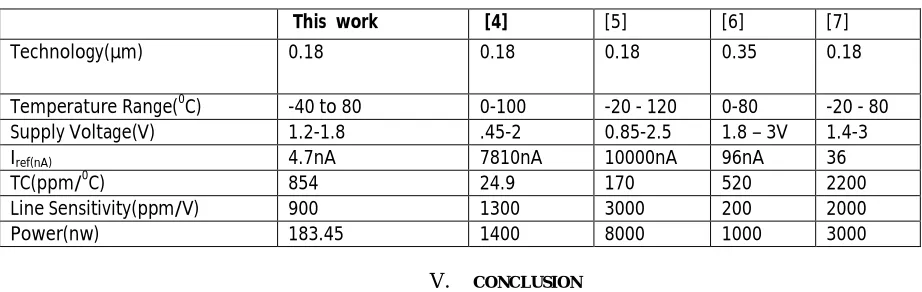
TABLE PERFORMANCE COMPARISON OF THIS WORK WITH RECENTLY PUBLISHED CURRENT REFRENCE CIRCUIT
This work [4] [5] [6] [7]
Technology(µm) 0.18 0.18 0.18 0.35 0.18
Temperature Range(0C) -40 to 80 0-100 -20 - 120 0-80 -20 - 80
Supply Voltage(V) 1.2-1.8 .45-2 0.85-2.5 1.8 – 3V 1.4-3
Iref(nA) 4.7nA 7810nA 10000nA 96nA 36
TC(ppm/0C) 854 24.9 170 520 2200
Line Sensitivity(ppm/V) 900 1300 3000 200 2000
Power(nw) 183.45 1400 8000 1000 3000
V. CONCLUSION
We have developed an ultralow-power CMOS current reference circuit consisting of subthreshold MOSFET circuit and no resistors.the device generates a temperature and supply voltage compensated reference current.our circuit generates a 4.715nA output current.the temperature coefficient and ine regulation of the output current were 854ppm/0C and 0.9%/V,respectively the power dissipation was about 0.18µW.our circuit will be useful as a current reference circuit for use in power-aware LSI applications,such as RFIDs,implantable medical devices,and smart sensor network.
REFERENCES
1) J.Lee and S.H. cho, “A 1.4µW 24.9ppm/0C current reference with process insensitive temperature compensation in 0.18µm CMOS,” IEEE J Solid-State circuits ,vol.48,no.10,2012.
2) W.Liu,W.Khalil,M.Ismail,and E.K ussener, “A Resistor-free Temperature Compensated CMOS current reference ,”Proc.2010 IEEE Int.Symp.circuits and systems(ISCAS),P.845,May-June 2010.
3) L.Magnelli,F.Crupi,P.Corsonello,C.Pace,and G.Iannaccone, “A 2.6nW,0.45V Temperature Compensated Subthreshold CMOS Voltage reference ,”.IEEE J.Solid State Circuits,vol.46,no.2,pp.465-474,2011.
4) Z.Hung,Q.Luo,and Y.Inoue, “A CMOS Sub 1-V nanopowercurrent and voltage reference with leakage compensation ,”.Proc.IEEE Int.Symp.Circuits and Systems(ISCAS),pp.4069-4072,2010.