Embedded
Microcontroller
System for
Bioimpedance
Measurements
Master thesis
Patrick Hisni
Brataas
June 2, 2014
Abstract vii
Acknowledgments ix
1 Introduction 1
1.1 Background and Motivation . . . 1
1.2 Goal of this Thesis . . . 1
2 Bioimpedance Theory 3 2.1 Basics . . . 3 2.1.1 Resistor . . . 3 2.1.2 Capacitor . . . 3 2.1.3 Bode plot . . . 4 2.1.4 Wessel plot . . . 4 2.2 Immittance . . . 4 2.2.1 Impedance . . . 4 2.2.2 Admittance . . . 5
2.2.3 Resistivity, conductivity, impedivity, admittivity, im-mittivity and perim-mittivity . . . 6
2.3 Bioimpedance . . . 6
2.3.1 Electrical properties of tissue . . . 6
2.3.2 Polarization . . . 9
2.3.3 Dispersion . . . 10
2.3.4 Equivalent electrical circuit for biological tissue and the Cole model . . . 10
2.4 Electrodes and Measurement . . . 13
2.4.1 Monopolar measurements . . . 13
2.4.2 Two electrode setup. . . 14
2.4.3 Four electrode setup . . . 14
2.4.4 Transfer immittance . . . 17
2.4.5 Three electrode setup . . . 17 i
ii CONTENTS
2.4.6 Electrode size and geometry . . . 18
2.4.7 Electrode noise . . . 18
2.4.8 Needle electrode. . . 20
3 Electronics Theory 23 3.1 Sine wave . . . 23
3.2 Direct Digital Synthesizer . . . 23
3.3 Current Measurements . . . 25 3.3.1 Shunt Ammeter . . . 27 3.3.2 Transimpedance Amplifier . . . 27 Feedback compensation. . . 28 3.4 Virtual Ground . . . 30 3.5 Decoupling capacitors. . . 30 3.6 Comparator . . . 31 3.7 AC coupling . . . 32 3.8 Analog-to-Digital Converter . . . 33 3.9 Operational Amplifier . . . 33 3.9.1 Voltage Follower . . . 34
3.9.2 Negative Feedback Amplification . . . 35
Non-inverting Amplifier . . . 35
Inverting Amplifier . . . 36
Advantages and Disadvantages . . . 36
3.10 Single Supply . . . 36
3.11 Noise in Analog circuits . . . 38
3.11.1 Thermal Noise . . . 38
3.11.2 Shot Noise (Schottky Noise) . . . 38
3.11.3 Flicker Noise . . . 39
3.12 Transimpedance Amplifier Noise Analysis. . . 40
4 Digital Theory 43 4.1 ARM . . . 43
4.1.1 What is ARM . . . 43
4.1.2 What is ARM Coretex-M3 . . . 43
4.1.3 Nested Vector Interrupt Controller (NVIC) . . . 43
4.1.4 Cortex Microcontroller Software Interface Standard (CM-SIS) . . . 44
4.1.5 CMSIS Digital Signal Processing Library . . . 44
4.2 STM32 . . . 44
4.2.1 Clock tree . . . 45
4.2.2 System clock . . . 46
4.2.4 Direct Memory Access (DMA) . . . 46
4.2.5 Memory Map . . . 47
4.2.6 Flash. . . 47
4.2.7 Standard Peripheral Library (SPL) . . . 47
4.2.8 Register names and bit definitions . . . 47
4.3 Microcontroller . . . 49
4.3.1 Debugging . . . 49
Using the debugger . . . 49
4.3.2 Interrupts . . . 50
4.3.3 printf(). . . 50
Retarget printf() to UART . . . 51
Use printf() with floating point numbers in CooCox . . 51
4.3.4 Using standard library math.h in CooCox . . . 52
4.4 Digital Signal Processing (DSP) . . . 52
4.4.1 Sampling theorem. . . 52
4.4.2 Undersampling . . . 53
4.4.3 Equivalent Time Sampling . . . 53
4.4.4 Finite Impulse Response Filter . . . 56
4.4.5 Digital Lock-in Amplifier . . . 58
4.4.6 4fs Technique . . . 60
4.4.7 Signal Averaging . . . 61
4.5 Fixed-point numbers . . . 62
4.6 Software Tools. . . 62
4.6.1 Software revision control system . . . 62
4.6.2 Differencing and merging tool . . . 63
4.6.3 MathWorks MATLAB . . . 63
4.6.4 ARM platform development tools . . . 63
GNU ARM Toolchain . . . 63
CooCox CoIDE . . . 64 4.6.5 Qt . . . 64 Qt framework . . . 64 Qt Creator IDE . . . 64 Qt and Android . . . 64 4.6.6 Python. . . 65
4.6.7 Software Version Overview . . . 65
4.7 Android / Java . . . 65
4.7.1 Android Manifest . . . 66
4.7.2 Java Native Interface . . . 66
4.7.3 Singleton design pattern . . . 66
iv CONTENTS
5 System Design: Hardware 69
5.1 Overview. . . 69
5.2 DDS . . . 70
5.3 Microcontroller Printed Circuit Board. . . 74
5.3.1 ST-LINK/V2 Programmer/Debugger . . . 74
5.4 Analog front-end . . . 74
5.4.1 Virtual Ground . . . 76
5.4.2 AC coupling and attenuation . . . 77
5.4.3 Comparator . . . 78
5.4.4 Three electrode excitation stage . . . 79
5.4.5 Transimpedance Amplifier . . . 79 5.4.6 Gain stages . . . 82 5.4.7 Decoupling capacitors . . . 83 5.4.8 Simulation . . . 84 5.4.9 Prototypes. . . 84 5.5 Bluetooth . . . 84
6 System Design: Software 89 6.1 Overview. . . 89
6.1.1 Modular code . . . 89
6.1.2 Code abstraction levels . . . 89
6.1.3 Code Organization . . . 91
6.1.4 Naming Conventions . . . 92
6.2 Microcontroller : Drivers . . . 92
6.2.1 ADC - Analog-to-Digital Converter . . . 92
6.2.2 DMA - Direct Memory Access . . . 93
6.2.3 DDS - Direct Digital Synthesizer . . . 94
6.2.4 EXTI - External Interrupt . . . 94
6.2.5 FLASH - Flash Memory . . . 94
6.2.6 GPIO - General Purpose Input Output . . . 94
6.2.7 IWDG - Independent Watchdog . . . 94
6.2.8 LED - Light Emitting Diode . . . 95
6.2.9 LSI - Low Speed Internal Oscillator . . . 95
6.2.10 NVIC - Nested Vector Interrupt Controller . . . 95
6.2.11 RCC - Reset and Clock Control . . . 96
6.2.12 SYSTICK - System Tick . . . 96
6.2.13 TIM - Timer . . . 96
6.2.14 UART - Universal Asynchronous Receiver/Transmitter 97 6.2.15 ZCD - Zero Crossing Detector . . . 97
6.3 Microcontroller : Interface . . . 97
6.3.2 DSP - Digital Signal Processing . . . 97 6.3.3 Initialize . . . 97 6.3.4 Measurements . . . 98 6.3.5 Message Parser . . . 98 6.3.6 Queues. . . 98 6.3.7 Timer . . . 98 6.3.8 User . . . 98 6.4 Microcontroller : Application . . . 99
6.4.1 BMS - Bioimpedance Measurement System. . . 99
6.5 Microcontroller : ISR - Interrupt Service Routines . . . 99
6.6 Microcontroller : Other . . . 100
6.6.1 System Event Loop . . . 100
6.6.2 Communication . . . 100
6.6.3 Measurement Implementation . . . 100
6.6.4 4fs method . . . 100
Digital Lock-in . . . 101
6.7 Graphical User Interface . . . 103
6.7.1 Overview . . . 103
6.7.2 main.cpp. . . 103
6.7.3 Bluetooth . . . 103
6.7.4 Bluetooth Device List . . . 105
6.7.5 Main Window . . . 105
6.7.6 Measurement Plots . . . 105
6.7.7 Receive . . . 105
6.7.8 Send . . . 106
7 System Verification and Calibration 107 7.1 Testing the DDS . . . 107
7.2 Testing the Analog Front-End . . . 108
7.3 Microcontroller Interrupts and Events . . . 108
7.4 ADC Calibration . . . 108
7.5 System Voltage Calibration . . . 111
7.6 Phase Calibration . . . 113
7.7 Measuring: Resistance . . . 114
7.8 Measuring: RC series . . . 114
7.9 Measuring: Boiled Egg . . . 117
7.10 Measuring: General Biological Materials . . . 118
8 Summary, Conclusion and Future Work 119 8.1 Conclusion of Present Work . . . 119
vi CONTENTS
References 121
A Microcontroller Code 123
A.1 Code: C . . . 123
B GUI Code 255 B.1 Qt Project file (.pro) . . . 255
B.2 Code: C++ . . . 257 B.3 Code: Java . . . 307 B.4 Code: XML . . . 314 C Python Code 319 D Matlab Code 323 E Schematics 331
In this thesis the design and prototype of a bioimpedance measurement sys-tem is described. The syssys-tem is wireless and battery powered. A custom analog front-end has been made to be able to do bioimpedance measure-ments. It uses a two or three electrode setup to do the measuremeasure-ments. It does most of the signal processing in the digital domain and two different techniques has been discussed. A common ARM microcontroller has been used to do the processing. The measurement data is transferred from the system to a desktop computer or Android device over Bluetooth.
The system has been tested and verified to work in the 1 kHz to 140 kHz frequency range. It measures the impedance modulus and phase cor-rectly when tested with an electrical circuit. The egg white, egg yolk and the boundary between has been successfully discriminated by using a needle electrode as the measurement electrode.
This thesis is the fullfilling of the Master of Science in Electronics and Com-puter Technology at the Department of Physics, University of Oslo. This work was carried out part-time from August 2012 to June 2014.
I would like to thank my supervisors Professor Ørjan G. Martinsen and Researcher Håvard Kalvøy for letting me undertake this project and for all feedback and help during the work on this thesis. A thanks to Oslo Bioimpedance Group for the trip to the International Conference on Elec-trial Bio-Impedance in Germany and the two day seminar at Sundvollen.
Thanks to the guys at the Electronics lab for all help.
It has been great being able to bounce ideas and ask questions to you Bent and thanks for the LaTeX template and valuable feedback.
At last I would like to thank my fantastic girlfriend Kristine for her infinite patience and understanding and my friends and family for their support during this time.
ADC Analog to Digital Converter
AF E Analog Front-End
AHB Advanced High Speed Bus
AN T Apache Another Neat Tool
AP B Advanced Peripheral Bus
AP I Application Programming Interface
BIBO Bounded-Input Bounded-Output
BLM Bilayer Lipid Membrane
BM S Bioimpedance Measurement System
CooCox Cooperate on Cortex
CP E Constant Phase Element
DAC Digital to Analog Converter
DIP Dual Inline Package
DM A Direct Memory Access
DSP Digital Signal Processing
EA Electrode Area
EEA Effective Electrode Area
EN BW Equivalent Noise Bandwidth
ET S Equivalent Time Sampling
xii ACKNOWLEDGMENTS
F EM Finite Element Method
F F T Fast Fourier Transform
F IF O First-In First-Out
F IR Finite Impulse Response
F P U Floating Point Unit
GBP Gain Bandwidth Product
GCC GNU Compiler Collection
GDB GNU Debugger
GN U GNU’s Not Unix
GU I Graphical user interface
HSE High Speed External
HSI High Speed Internal
I2C Inter-Integrated Circuit
IC Integrated Circuit
IDE Integrated Development Environment
IIR Infinite Impulse Response
IRQ Interrupt Request
ISR Interrupt Service Routine
IW DG Independent Watchdog
J DK Java Development Kit
J T AG Joint Test Action Group
M inGW Minimalist GNU for Windows
N DK Native Development Kit
P ID Proportional Integral Derivative
P LL Phase Locked Loop
QM L Qt Meta/Modeling Language
RC Resistor Capacitor
RISC Reduced Instruction Set Computer
RM S Root Mean Square
ROM Read Only Memory
RSS Root Sum Square
RT C Real Time Clock
RT OS Real Time Operating System
SDK Software Development Kit
SN R Signal-to-Noise Ratio
SP L Standard Peripheral Library
T IA Transimpedance Amplifier
2.1 Concentration of electrolytes in intra-cellular and extra-cellular liquids in milliequivalents per liter. Taken from (Grimnes and Martinsen, 2008, p. 24) . . . 7
2.2 At low frequencies (LF), the extracellular path dominates due to the capacitive properties of the cell membrane. At high frequencies (HF) the cells capacitive properties allows the AC current to pass through. Taken from (Grimnes and Martinsen, 2008, p. 103) . . . 8
2.3 Idealized dispersion regions for tissue. DC conductance have been subtracted from the imaginary part of the complex per-mittivity 00r value. Taken from (Martinsen et al., 2002) . . . . 10
2.4 The frequency regions and mechanisms that corresponds to the different dispersions. Taken from (Grimnes and Martinsen, 2008, p. 90) . . . 11
2.5 Electrical model of biological material. Taken from (Ivorra, 2003) . . . 11
2.6 Wessel plot. Notice that the reactance-axis have been inversed. This is often seen in Wessel plots. Redrawn from (Nordbotten, 2008, p. 11) and modified. . . 13
2.7 The arrows shows the current density and the color the po-tential distribution in this two-electrode configuration. a) Equal and symmetrical electrodes. b) Quasi-monopolar setup with non-symmetrical electrode configuration. Taken from (Kalvoy, 2010). . . 14
2.8 Four-electrode configuration on the underarm with the cur-rent carrying electrodes placed as outer electrodes and pick-up electrodes as inner electrodes. Taken from (Grimnes and Martinsen, 2006) . . . 15
2.9 Shows the sensitivity area for a four-electrode setup in an infi-nite homogenous material. The dark blue indicate areas with negative sensitivity. Taken from (Kalvoy, 2010) . . . 16
xvi LIST OF FIGURES
2.10 Shows the sensitivity area for a three-electrode setup in an
infinite homogenous material. Taken from (Kalvoy, 2010) . . . 19
2.11 Two common skin surface electrode designs. EA is the elec-trode area and EEA is the effective elecelec-trode area. Taken from (Grimnes and Martinsen, 2006) . . . 19
2.12 Electrical potential distribution and sensitivity field of a needle electrode in a saline solution. The scale on the right shows the voltage factor, where 1.0 is the maximum voltage which can be found on the needle electrode. Taken from (Kalvoy, 2010) . 21 3.1 Sine wave with the most commen sine wave characteristics. . . 24
3.2 The building blocks of a DDS . . . 26
3.3 Basic shunt ammeter . . . 27
3.4 Basic transimpedance amplifier. . . 28
3.5 Transimpedance amplifier with compensation. . . 29
3.6 A voltage divider. . . 31
3.7 A comparator.. . . 32
3.8 A non-inverting AC coupling circuit. . . 33
3.9 An operational amplifier. . . 34
3.10 A voltage follower. . . 34
3.11 A non-inverting operational amplifier. . . 35
3.12 An inverting operational amplifier. . . 36
3.13 A biased AC coupled inverting operational amplifier. . . 37
4.1 STM32 clock tree. Taken from (STM32, 2011a, p. 90) . . . 45
4.2 STM32 memory map. Taken from (STM32, 2011b, p. 38) . . . 48
4.3 ISR code example. . . 51
4.4 A 1 Hz and 19 Hz signal sampled at 20 Hz where the red and blue dots shows the 20 Hz samples respectively. . . 54
4.5 The reconstructed 1 Hz and 19 Hz signal . . . 55
4.6 An example of an ETS signal. . . 57
4.7 Block diagram of a digital lock-in amplifier. . . 59
4.8 Block diagram of a digital lock-in amplifier using this technique. 61 5.1 Hardware design overview. . . 69
5.2 An image of the DDS module. . . 71
5.3 DDS input/output overview. . . 72
5.4 DDS signal amplitude as function of frequency. . . 73
5.5 The programmable register of the AD9850. . . 73
5.6 Image of the microcontroller PCB. . . 75
5.8 Virtual ground circuit used in the hardware prototypes. . . 77
5.9 The AC coupling and attenuation stage used in the hardware prototypes. . . 78
5.10 The comparator stage used in the hardware prototypes. . . 79
5.11 The electrode interface stage used in the hardware prototypes. 80 5.12 The transimpedance amplifier stage used in the hardware pro-totypes. . . 80
5.13 The gain stage used in the hardware prototypes. . . 83
5.14 Magnitude and phase plot of the simulated circuit. . . 85
5.15 A picture of the first/second prototype. . . 86
5.16 A picture of the third prototype. . . 87
5.17 A picture of the Bluetooth module. . . 88
6.1 Code abstraction levels. . . 90
6.2 Shows the message format of an incoming measurement set-tings message. . . 101
6.3 An overview of the used hardware and driver modules for the two measurement techniques. . . 102
6.4 A block diagram of the 4fs technique algorithm. . . 102
6.5 An image of the GUI. . . 104
7.1 A screenshot from the logic analyzer software from Saleae. . . 109
7.2 Showing the ADC values before and after calibration. . . 110
7.3 Showing the resistance offset before and after system voltage calibration. . . 112
7.4 Before and after the phase calibration on a resistor. . . 115
7.5 The calculated and measured phase as function of resistance in a RC series circuit. . . 116
7.6 The values measured on egg white and egg yolk. . . 118
E.1 Excitation part of the analog front-end. . . 332
4.1 List of software and versions used. . . 65
5.1 Hardware interconnection overview. . . 70
5.2 DDS requirements. . . 70
5.3 Table of decoupling capacitors used. . . 83
6.1 List of drivers implemented. . . 91
6.2 List of interfaces implemented. . . 91
6.3 List of ISRs implemented. . . 92
6.4 Naming conventions used in the microcontroller C code in this thesis. . . 93
7.1 Table with DDS peak-to-peak amplitude output between 1 kHz and 140 kHz. . . 107
7.2 Table of egg discimination limits set. . . 118
Chapter 1
Introduction
1.1
Background and Motivation
Commercial instruments for measuring bioimpedance is often large and ex-pensive. A small, lightweight and cheap device with a more specific use in mind is in many cases more desirable. If it were to be used for a single or a few clinical application the device can be optimized for this use.
Designing a platform from scratch ensures it is very flexible and can serve as a platform for future development. The limits for what can be achieved with microcontrollers are continuously pushed and this makes it possible to implement more functionality.
Using a computer, tablet or mobile device to visualize data is becoming more and more popular, especially the two latter.
1.2
Goal of this Thesis
It was desired to design a small wireless and battery powered device to mea-sure bioimpedance in biological materials. The device should do the process-ing in the digital domain on a microcontroller, and send the data wirelessly to a connected device for visualization. The ultimate goal was to be able to show that this system could successfully discriminate between different biological materials.
The goal can be divided into three parts:
1. Develop a microcontroller system that successfully measures impedance. 2. Develop software that wirelessly receive the impedance data and
visu-alizes it on a display.
3. Successfully discriminate between some biological tissues using a needle measurement electrode.
Chapter 2
Bioimpedance Theory
This chapter gives an introduction to basic bioimpedance theory.
2.1
Basics
2.1.1
Resistor
A resistor is simply a passive electrical component that reduces current flow and indirectly the voltage. This is because the current and voltage are di-rectly proportional in a resistor. This leads to Ohm’s law:
V =RI (2.1)
where V is the voltage across the resistor, R is the resistance of the resistor and I the current flowing through.
2.1.2
Capacitor
A capacitor is comprised of two conductors that is separated by air or some kind of material. The material separating the two conductors is called a di-electric. When a voltage is applied over a capacitor, it will charge and the relationship between how much it charges and the voltage is called capaci-tance. Its equation is usually written:
C= Q
V (2.2)
where C is the capacitance, Q is the charge and V the voltage. The type of dielectric and the geometry of the capacitor determines the capacitance.
2.1.3
Bode plot
A bode plot shows the magnitude response and phase as a function of fre-quency. The x-axis is frequency in logarithmic scale. This plot gives a good overview of how magnitude and phase varies with frequency.
2.1.4
Wessel plot
A Wessel plot displays the real and imaginary part of the immittance as the x-axis and y-axis respectively. This if often seen in the field of bioimpedance when comparing and fitting experimental results with the Cole model.
2.2
Immittance
Immittance is a more general term meaning impedance or admittance for those cases where differentiating between the two has no value. Since Immit-tance is just a term, it does not have its own unit.
2.2.1
Impedance
Before we can address bioimpedance, we must know what impedance is. In this thesis it is implied that when using the word impedance it is referring to
electrical impedance. Impedance is measured in Ohms [Ω] and is a measure
of how well, for example, an electrical circuit oppose the resulting alternating current when an alternating voltage is applied to it. This ratio can be written as:
Z = v
i (2.3)
where v is the applied voltage and i is the current. Written in the Carte-sian form, impedance consists of two parts:
Z =R+jX (2.4)
where the real part R is the resistance and the imaginary part X is the reactance. If written in complex exponential form:
Z =|Z|ejθ (2.5)
|Z| is the magnitude and θ the phase difference between the voltage and
current in the time domain. These two forms express the same and the calculation from one form to the other is trivial:
2.2. IMMITTANCE 5 |Z|=√R2+X2 (2.6) θ=arctan(X R) (2.7) R=|Z|cos(θ) (2.8) X =|Z|sin(θ) (2.9)
2.2.2
Admittance
Admittance is measured in Siemens [S] and is the inverse of impedance. This is a measure of how well, for example, an electrical circuit conducts current. The admittance can be measured when applying an alternating current and measuring the resulting alternating voltage. This results in the ratio:
Y = 1
Z = i
v (2.10)
where i is the applied current and v the voltage. Written in Cartesian form we get:
Y =G+jB (2.11)
where the real part G is the conductance and the imaginary part B is the susceptance. In addition, like impedance, admittance can be written on the complex exponential form. By using complex numbers theory it can be shown that it is possible to convert to impedance to admittance and vice versa. The resulting equations for the conversions are:
Impedance to admittance: G= R R2+X2 (2.12) B =− X R2+X2 (2.13) Admittance to impedance: R= G G2+B2 (2.14) X =− B G2+B2 (2.15)
2.2.3
Resistivity, conductivity, impedivity, admittivity,
immittivity and permittivity
Resistance is dependent on both the materials resistivity and geometry:
R =ρG (2.16)
where R is the resistance, ρ the resistivity and G the geometry. In for
example a cylindrical resistor the resistance is given as:
R=ρ l
A (2.17)
where l is the length of the cylinder and A is the cross-sectional area. A similar dependency is found for a parallel plate capacitors capacitance and permittivity:
C =G=A
d (2.18)
where C is the capacitance, is the permittivity, A the plate area and d
is the distance between the plates.
This means the –ance suffix parameters are dependent on both the electri-cal properties of the material and the geometry, while the –ivity suffix implies parameters that only depend on the electrical properties of the material itself,
not the geometry. (Grimnes and Martinsen, 2008, p. 2)
2.3
Bioimpedance
Bioimpedance is the term used when referring to the impedance of a bio-logical substance. Bioimpedance describes the passive electrical properties of biological materials. Unlike metals where the charge carriers are the free electrons, in biological materials the charge carriers are the ions in the intra-cellular and extra-intra-cellular liquids. The most important ions are K+ and Na+
as can be seen in table 2.1.
Since ions are the charge carriers, a current flow implies a movement of substance, which in itself results in changes in the biological material. Hence, a DC current would change the conductor itself, first at the electrodes, but
over time in the whole material. (Grimnes and Martinsen, 2008, p. 8))
2.3.1
Electrical properties of tissue
The cell membrane is a poor electrical conductor due to phospholipids form-ing a bilayer lipid membrane (BLM) and acts as a dielectric, which means
2.3. BIOIMPEDANCE 7
Figure 2.1: Concentration of electrolytes in intra-cellular and extra-cellular
liquids in milliequivalents per liter. Taken from (Grimnes and Martinsen,
2008, p. 24)
the cells have capacitive properties. The conductivity of the membrane itself is very low and the membrane is only about 7 nm thick. Because of this, the
cell has a very high capacitance of about 1 cmµF2. (Grimnes and Martinsen,
2008, p. 100) Due to the diffusion of ions through the cell membrane, the
concentration of ions in the intracellular and extracellular liquids can change. The migration of ions through the membrane is possible due to ion channels. These channels are ion specific.
At DC and low frequencies the current flows around the cells in the extra-cellular liquids, at higher frequencies the cell membrane capacitance allows AC current to pass through. For frequencies in between there will be a mix of how much goes around and through the cell. Approximate values for low, medium and high frequencies in this context is less than 10 kHz, 100 kHz and
above 1 MHz respectively. This is shown in figure2.2. Biological tissue also
have inductive properties, but these are insignificant at frequencies below 10
MHz (Riu, 2004) and not further discussed in this thesis.
In general, the impedance of tissue decreases with an increase in fre-quency.
Biological tissue is a very heterogeneous material and different tissues like muscles, fat, organs, body fluids etc. can have very different cell structures. This includes cell size and shape, how they are joined together and how much e.g. extracellular liquid that is present in a specific tissue. Adipose tissue has little extracellular electrolytic liquid for conduction of lower frequencies while skeletal muscles might have anisotropic (direction dependent) properties.
Figure 2.2: At low frequencies (LF), the extracellular path dominates due to the capacitive properties of the cell membrane. At high frequencies (HF) the cells capacitive properties allows the AC current to pass through. Taken
2.3. BIOIMPEDANCE 9
2.3.2
Polarization
Polarization is the disturbance in the charge distribution in a region as a result of an induced electric field. This means the charge does not change while the distribution of charge does. Since transport of ionic current also means that substance will be moved, there will be concentration changes in the biological material near the electrodes. In the field of bioimpedance, the measuring methods used are exogenic. This means energy is applied to a system, which will polarize it. The energy applied can be both be stored and dissipated in a dielectric medium. All materials are polarizable, altough to different degrees. This includes conductors and insulators. An electric dipole is a separation of positive and negative charges. An example of a dipole is a water molecule which has a negative and positive pole. Dielectric theories regarding biomaterials often consider them as either polar materials or as inhomogeneous materials with interfacial polarization contributions. (Grimnes and Martinsen, 2008, p. 58) The polarization is the sum of three components:
1. Number of induced dipoles due to an applied external field.
2. Orientation of the already existing permanent dipoles in the direction of an applied electric field.
3. The permanent dipole moment when no electric field is present.
There is also an important difference between electronic polarization and ionic polarization. Electronic polarization is a displacement of the electron cloud with respect to the nucleus (protons). Ionic polarization is the dis-placement of positive ions with respect to the negative ions.
Polarization of biological materials does not occur instantaneously. When applying an AC signal the frequency is critical for how much polarization we will observe, depending on the time the charges need to change their positions in the material. If the frequency is low enough it will mean that all charges have enough time to change their position and the polarization will be maximal. For the same reason, polarization will decrease with increasing frequency. The time dipole molecules need to reorient themselves is called relaxation time and has a relaxation time constant. This can be seen in the time domain. In the frequency domain when plotting permittivity as a function of frequency, one can see the effect of relaxation. This characteristic is called dispersion.
2.3.3
Dispersion
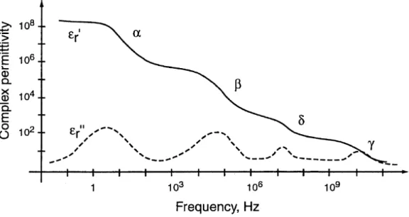
Frequency dispersions can be found when measuring on biological materi-als. Dielectric dispersion is the dependency between the permittivity and frequency in a material when we polarize it. There is also a lag between the polarization and the changes in the applied electrical field. Three dispersion
areas were described by Schwan in 1957 and named α, β and γ. Later a
fourth dispersion area between β and γ has been described and named δ.
The typical idealized dispersion regions for tissue can be shown in figure2.3.
(Martinsen et al., 2002) Different tissue have different degrees of dispersion.
For example, muscle tissue exhibits a largeα-dispersion while blood does not
have one.
Figure 2.3: Idealized dispersion regions for tissue. DC conductance have been
subtracted from the imaginary part of the complex permittivity 00r value.
Taken from (Martinsen et al., 2002)
Many mechanisms contribute to these dispersions and in table 2.4 one
can see the approximate frequency regions for the different dispersions and what mechanisms responsible are.
2.3.4
Equivalent electrical circuit for biological tissue
and the Cole model
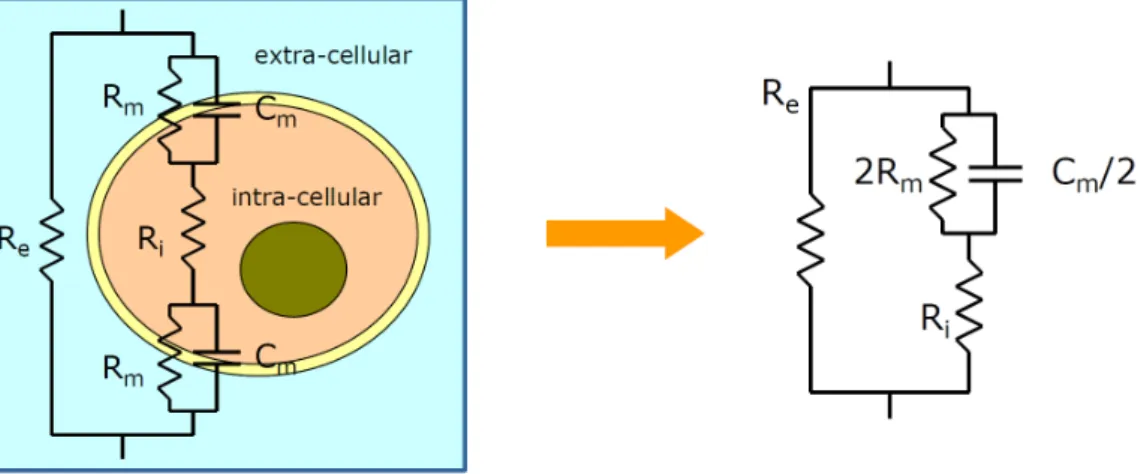
The cell bioimpedance and tissue bioimpedance can be modeled by using an equivalent electrical circuit. Many of these models exists, but one of the most
2.3. BIOIMPEDANCE 11
Figure 2.4: The frequency regions and mechanisms that corresponds to the
different dispersions. Taken from (Grimnes and Martinsen, 2008, p. 90)
common model is displayed in figure 2.5.
Figure 2.5: Electrical model of biological material. Taken from (Ivorra,2003)
The circuit on the right in figure 2.5 is equivalent to the left after some
simplifications. (Ivorra, 2003) As shown, the current can flow through the
extracellular liquid (Re), through the bilayer lipid membrane (Cm) or across
the ionic channels (Rm). Once the current has entered the cell it also travels
through the intracellular liquid (Ri) and across the cell membrane (Rm||Cm).
Rm is often omitted as the cell membrane is a poor conductor. This model is
also often seen as an equivalent model in the literature. This model only has a single dispersion, but tissue often have more than one dispersion overlapping in some of the frequency area. This requires a more complex model where the capacitor in the previous model is substituted by a Constant Phase Element
(CPE). The CPE is not an electronic component that exists, but is described as a frequency dependent capacitor and resistor. It can be modeled so that
the phase is frequency independent. (Grimnes and Martinsen, 2008, p. 299)
It is also called a fractional capacitor. CPE has the impedance:
ZCP E =
1
(j2πf C)α (2.19)
where j is the imaginary unit, f the frequency, C the capacitance and α
a parameter with a value usually between 0.5 and 1. When α =1 the CPE
behaves identical to an ideal capacitor and when α =0 it behaves like an
ideal resistor. When we substitute Rm and Cm with CPE in the circuit in
figure 2.5 we get the impedance expressed as:
Z =R∞+
R0−R∞
1 + (j2πf τ)α (2.20)
This equation is called the Cole equation. (Cole, 1940) R∞ = Ri is the
resistive part at infinite frequency,R0 is the impedance at 0 Hz,τ is the time
constant(∆RC)1α (Elwakil and Maundy,2010) where∆R =Rm =R0−R∞
and α the CPE parameter.
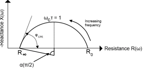
Different tissues can be characterized by finding these four parameters. These four parameters can be found by measuring with an impedance
ana-lyzer and plotting the values in a Wessel plot, like in figure 2.6.
The real part in figure 2.6 is the resistance and the imaginary part the
reactance. R0 and R∞ can be found where the arc intersects the Z
0 -axis. The CPE angle can be found as the angle between the tangent along the arc
atR∞ and the R-axis. α can now be calculated as:
α= 2ϕCP E
π (2.21)
τ can be found by finding the frequency where |X| has its maximum
value. τ is then calculated as:
τ = 1 2πf|X|max
(2.22) When more than one dispersion occurs, the Cole equation can be ex-panded: Z =R∞+ (R0 −R∞)1 1 + (j2πf τ1)α1 + (R0−R∞)2 1 + (j2πf τ2)α2 +... (2.23)
2.4. ELECTRODES AND MEASUREMENT 13
Figure 2.6: Wessel plot. Notice that the reactance-axis have been inversed.
This is often seen in Wessel plots. Redrawn from (Nordbotten, 2008, p. 11)
and modified.
2.4
Electrodes and Measurement
To be able to measure bioimpedance an interface between the biological sam-ple and the electronics is needed. Electrodes provide this interface. At the electrode is where the shift in charge carriers occur. Between the free flow-ing electrons in the metal to the ions in the biological material and vice versa. This means the electrode is a transducer, converting a physical quan-tity (ions) into an electric signal. A pair of electrodes can be used to carry current, measuring a potential difference with no current flowing or both. (Grimnes and Martinsen, 2008, p. 253) At the interface between the metal and electrolyte, the AC current flow is impeded to some degree and this cre-ates a polarization impedance. Therefore, when current flow in the electrode wire the electrode is polarized. There are many ways to design and configure the electrodes. This is in many applications critical for correct measurements. The most common electrode configurations are 2-, 3- and 4- electrode setups.
2.4.1
Monopolar measurements
When using two or more electrodes one can achieve monopolar measurements by making one of the electrodes dominant. This can for example be done in a two-electrode setup by increasing or decreasing the size of one of the
shows two equal electrodes in a symmetrical bipolar system and figure 2.7b
shows a quasi-monopolar system. In figure2.7b the sensitivity and therefore
the impedance contribution is closer to the small measuring electrode than
in figure2.7a and the impedance contribution from the large electrode would
be insignificant.
Figure 2.7: The arrows shows the current density and the color the potential distribution in this two-electrode configuration. a) Equal and symmetrical electrodes. b) Quasi-monopolar setup with non-symmetrical electrode
con-figuration. Taken from (Kalvoy, 2010)
2.4.2
Two electrode setup
In a two-electrode setup, the same pair of electrodes are used to both excite and measure. The immittance of the system is measured and includes the whole setup. This means the electrodes, electrode interfaces, leads and the sample to be measured are all connected in series and will affect the mea-sured immittance. The impedance can be meamea-sured by applying a controlled current signal and measuring the voltage and vice versa for admittance.
2.4.3
Four electrode setup
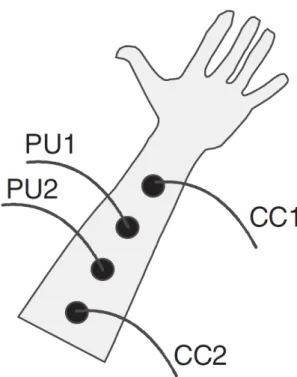
A four electrode setup uses two pairs of electrodes and is a two-port network with four terminals. One pair for current carrying and one pair for pick up.
This can be seen in figure 2.8 where CC1 and CC2 is the current carrying
electrodes and PU1 and PU2 the pick-up electrodes. The pick-up electrodes are usually connected to a very high impedance operational amplifier, which means in practice that no current will flow past these electrodes. When no
2.4. ELECTRODES AND MEASUREMENT 15
current flows through an electrode it will not be polarized. This means that when using the four electrode setup the electrode polarization impedance
will not be affecting the measurements. This setup is popular, but also
has its pitfalls and are more vulnerable to errors than monopolar and bipolar
setup. (Grimnes and Martinsen,2006) One of the pitfalls is zones of negative
sensitivity. This means that when measuring on heterogeneous materials it is possible that the measurements can have large errors. If the electrodes
are placed as shown in figure 2.8 it is often believed that only the volume
between the pick-up electrodes are measured. This is not true as the area between the pick-up electrode and the current-carrying electrode will have
negative sensitivity. If the impedivity is increased in this area the total
measured impedance will be lower and might not give the expected result. The negative sensitivity area of a four-electrode setup can be seen in a finite element method (FEM) simulation where the measured material is infinite
and homogenous. This is shown can be seen in figure 2.9.
Figure 2.8: Four-electrode configuration on the underarm with the current carrying electrodes placed as outer electrodes and pick-up electrodes as inner
Figure 2.9: Shows the sensitivity area for a four-electrode setup in an infinite homogenous material. The dark blue indicate areas with negative sensitivity.
2.4. ELECTRODES AND MEASUREMENT 17
2.4.4
Transfer immittance
It is important to be aware that a three and four electrode setup measures transfer immittance. This is because they are both a two-port network. For example if an electric current excitation signal is applied and the response is a voltage, we measure transfer impedance. Visa versa for transfer admit-tance. Transfer immittance distinguishes itself from immittance as it shows how much of the applied signal is sensed at the measuring electrodes. When we apply a current excitation signal, increasing the distance between the measuring electrodes and the electrodes where the current excitation signal is applied, will result in a smaller potential difference and impedance. When moved infinitely far apart the material in between seems to have zero re-sistance. This is clearly not correct and this behavior is very important to
be aware of when using these kind of electrode configurations. (Martinsen
and Grimnes, 2008) So it is not actually the impedance of the material it-self that is measured and finding resistivity, conductivity and permittivity is
practically not possible in an inhomogeneous material. Figure2.8 shows the
current carrying electrodes as the inner electrodes and the pick-up electrodes as the outer electrodes. It does not matter if they are interchanged as the reciprocity theorem guarantees that the same immittance will be measured
under linear conditions. (Grimnes and Martinsen, 2006)
2.4.5
Three electrode setup
A three electrode setup uses three electrodes where two are current carrying electrodes and one is a pick-up electrode. This means it is a two-port network with three terminals. The current carrying electrodes are shown as M and C
in figure2.10. The pick-up electrode is electrode R. The measuring electrode
M measures the potential between itself and the reference electrode R which is guaranteed to have the same potential as the excitation voltage.
Because the input impedance of the operational amplifier is very high, no current flows through the reference electrode. This means its contribution to the measurement is very small and no electrode polarization impedance since no current flow. This property makes it easier make a monopolar system by making the measuring electrode smaller, since the size of the reference and current carrying electrode C is less crucial. In this monopolar three-electrode setup the transfer immittance between the measurement electrode and the reference is measured and most of the contribution is from areas close to the measurement electrode. The electrode polarization impedance from electrode M is also included in the measurement. The monopolar characteristics can
The circuit in figure 2.10 does remove the 50/60 Hz mains noise that the material measured on picks up, as the current carrying electrode C and the operational amplifier it is connected to will compensate for it, without interfering with the measuring electrode.
If swapping the wires connecting electrode R and C the measured immit-tance should not change. This is guaranteed by the reciprocal theorem. If it does change then one of the electrodes might be too small and be in the non-linear region. This is an important test to ensure that the polarization impedance of electrode C and impedance of R does not contribute to the measurement.
If the metals of the R and M electrode is not the same, a DC potential will be generated. This is rarely wanted and care should be taken ensuring they are of the same material, especially when the same type of electrode cannot be used at both sites. This problem also arises if the tissue connected to generates an endogenic DC potential. The material measured on will then be under constant polarization as the operational amplifier will compensate for the potential difference trying to drive the inputs to zero volt difference. Combining the three electrode setup with making the relative size of the measurement electrode much smaller than the reference electrode increases the effect of the monopolar measurement.
2.4.6
Electrode size and geometry
Both noise and what is measured is affected by the size and geometry of the electrode. Two common skin surface electrode designs are shown in figure
2.11. Here the metal-electrolyte interface area is called electrode area (EA)
and the electrolyte-skin interface area is called the effective electrode area (EEA). EA determines the polarization impedance and EEA determines the skin impedance. Large EA implies low electrode polarization impedance. Large EEA on a measuring electrode implies an averaging effect and loss of spatial resolution. Large EEA on a stimulating electrode implies higher
excitable tissue volume. (Grimnes and Martinsen, 2006,2008)
2.4.7
Electrode noise
According to (Grimnes and Martinsen, 2008, p. 264) there are three rules
that are important regarding electrode noise:
1. Less noise the larger the electrode area, because of the averaging effect. 2. The more the electrode is polarizable, the more noise it will generate.
2.4. ELECTRODES AND MEASUREMENT 19
Figure 2.10: Shows the sensitivity area for a three-electrode setup in an
infinite homogenous material. Taken from (Kalvoy, 2010)
Figure 2.11: Two common skin surface electrode designs. EA is the electrode
area and EEA is the effective electrode area. Taken from (Grimnes and
3. A more diluted contact electrolyte will generate more noise.
In addition to this, sudden spikes of millisecond duration and hundreds of microvolt amplitude can be generated. Also a non-uniform electrode surface will generate noise.
2.4.8
Needle electrode
One of many invasive electrodes is the needle electrode. When this electrode is used in a monopolar setup where the other electrodes are relatively much larger, only the material’s impedance very close to the needle contribute to the measured impedance. A FEM calculation of this have been tried by (Hoyum et al., 2010). An insulated needle was placed in a saline solution and the measurement frequency was 100 kHz. The insulated needle had an active electrode area of 0.3 mm2 and the thickness of the insulation was
about 26 µm. More about the boundary conditions and material constants
can be found in (Hoyum et al., 2010) and more about general impedance of
needle electrodes can be found in (Kalvoy et al., 2010). Figure 2.12 shows
the sensitivity field from the simulation. A 97% sensitivity radius at 3.75 mm and 77.3% sensitivity radius at 1 mm. This shows that the part of the material very close to the needle electrode largely determines the immittance measured. This effect can be utilized to do for example tissue discrimination. More about tissue discrimination using needle electrode can be found in (Kalvoy et al., 2009).
2.4. ELECTRODES AND MEASUREMENT 21
Figure 2.12: Electrical potential distribution and sensitivity field of a needle electrode in a saline solution. The scale on the right shows the voltage factor, where 1.0 is the maximum voltage which can be found on the needle electrode.
Chapter 3
Electronics Theory
3.1
Sine wave
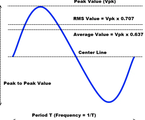
The sine wave is often seen in AC applications. In this section the relationship between different parameters describing the sine wave will be examined.
The peak value of a sine wave is is often labelled Vp or Vpeak and is the
top/bottom value of the sine wave from the center line. The average value is calculated by only taking the average of a half cycle as the average of a full cycle would be zero. The relationship between the average and the peak is:
Vavg =Vp ·0.637 (3.1)
The connection between the peak value and the root mean square (RMS) is:
Vp = √
2·VRM S (3.2)
If an AC current or voltage has a RMS value of 5 volts or ampere respec-tively, this is equal to the power in a DC current or voltage with the same current or voltage.
Equation 3.1 and 3.2 shows that the relation between the RMS and
av-erage can be written as:
VRM S =Vavg·1.11 (3.3)
3.2
Direct Digital Synthesizer
The DDS outputs a sinusoidal signal with a frequency that is set by a digital numeric control. The DDS requires an external timing reference, e.g. a
3.3. CURRENT MEASUREMENTS 25
crystal oscillator. This clock will be the sampling clock of the DDS. The frequency output range of a DDS is normally from DC to half of the external clock frequency.
A DDS consists of three building blocks. The accumulator, sine lookup table (angle-to-amplitude converter) and a digital-to-analog converter. This
can be seen in figure3.2.
The accumulator increments a number on each clock pulse resulting in a
ramp as shown in figure 3.2. The accumulator is often 12 to 24 bits. When
the accumulator overflows, one period of a sinusoidal signal is achieved and the accumulator starts incrementing from the reminder value, if any. This means that the larger the increment is, the faster it will overflow and higher the output frequency. The size of the increment is one of the inputs to a DDS and is often called the frequency (tuning) word.
The value output by the accumulator always corresponds to a phase be-tween 0 and 360 degrees. The sine lookup table simply converts the phase angle to a corresponding amplitude by looking up the phase angle in a read-only memory (ROM) and output the amplitude. This creates a discrete sinusoidal signal on the angle-to-amplitude converters output. This can be
seen in figure3.2.
The digital-to-analog converter (DAC) converts the discrete digital sinu-soidal signal to a continuous analog sinusinu-soidal voltage or current signal as
seen in figure3.2.
Even though usually not a part of the DDS, a low pass filtering circuit is added after the DDS output to smooth the analog sinusoidal waveform and remove unwanted harmonics/images.
The output frequency fout of the DDS is:
fout =
fclkFw
2N (3.4)
where fclk is the external clock frequency, Fw the frequency word and N
the number of accumulator bits.
3.3
Current Measurements
Two basic techniques used for measuring small currents are the shunt
amme-ter and the transimpedance amplifier (Keithley Instruments, 2004, c. 1.5.2).
Ac
cu
m
ula
to
r
Sin
e L
oo
ku
p
Ta
ble
Dig
ita
l-to
-An
alo
g
Co
nv
erte
r
Lo
w
P
as
s
Filte
r
Ex
te
rn
al
Clo
ck
Fre
qu
en
cy
W
ord
DD
S
Figure 3.2: The building blo cks of a DDS3.3. CURRENT MEASUREMENTS 27
3.3.1
Shunt Ammeter
A shunt ammeter can be made by placing a shunt resistor on the positive
input of a voltage follower. The basic circuit will look like in figure 3.3.
Rs
I
Vout
Figure 3.3: Basic shunt ammeter
Because of the high input impedance of the operational amplifier, the
input current I flows through the shunt resistor Rs creating a potential on
the positive input. The op-amp will try to keep the same potential on both
inputs and the output voltage Vout is then:
Vout =IRs (3.5)
The shunt resistor value should be made just big enough to ensure that the wanted voltage output is received. Some of the advantages of a lower shunt resistor value is better accuracy, time and temperature stability and
lower input time constant, but lower signal-to-noise (SNR) ratio (Keithley
In-struments, 2004, c. 1.5.2).
3.3.2
Transimpedance Amplifier
The transimpedance amplifier is a inverting negative feedback operational amplifier where the current signal is provided on the negative input. This is
Rf
I
Vout
Figure 3.4: Basic transimpedance amplifier.
In this circuit the input current I flows through the feedback resistorRf.
If the op-amp has a relative low input offset current the output voltage Vout
is:
Vout =−IRf (3.6)
In this circuit, the size of the output signal is directly proportional to
the feedback resistorRf. The voltage burden is low and the high gain
band-width product (GBP) of the operational amplifier ensures higher frequency operation than the shunt ammeter.
Feedback compensation
To increase the stability, bandwidth and reduce ringing on the output signal of a transimpedance amplifier, feedback compensation is used. Feedback
compensation is done using a feedback capacitor Cf in parallel with the
feedback resistor Rf, as shown in figure 3.5.
To ensure stability, a capacitor value that provides a phase margin of
at least 45 degrees should be calculated. TI (2013). Phase margin is 180
3.3. CURRENT MEASUREMENTS 29
Rf
I
Vout
Cf
of an amplifier. The value of the feedback capacitor Cf with a 45 degrees
phase margin is:
Cf =
s
Cs+Ci
2πRffGBP
(3.7)
where Cs and Ci is the shunt and input capacitance and fGBP the gain
bandwidth product.
The cut-off frequency calculation for a transimpedance amplifier is not done the same way as with an inverting amplifier. If it were, using a high
value feedback resistor like a 1MΩ with an op-amps with large GBP would
still only give a bandwidth in the thousands of hertz.
The transimpedance amplifiers cut-off frequency (-3dB), if the feedback
capacitor is calculated using equation 3.7, is:
f−3dB =
s
fGBP
2πRfCf
(3.8)
It is recommended by Bhat (2012) to overcompensate to provide
suffi-cient guardband to account for the up to ± 40 % variations in an op-amp’s
bandwidth and feedback capacitors tolerance.
3.4
Virtual Ground
Virtual ground is a steady reference potential that is different from ground. The simplest virtual ground reference can be made using a voltage divider
as shown in figure 3.6.
Here the output voltage Vout is:
Vout= R2 R1+R2
Vin (3.9)
where Vin is the input voltage and R1 and R2 the resistor values. A
voltage follower can be cascaded after the voltage divider to assure lower output impedance and more stable output reference voltage.
3.5
Decoupling capacitors
Decoupling capacitors (also called bypass capacitors) are used to reduce the effect noise has on a circuit element. A decoupling capacitor is connected as a shunt as close as possible to the circuit elements power supply pin. Most
3.6. COMPARATOR 31
R1
R2 Vin
Vout
Figure 3.6: A voltage divider.
circuit elements ideally want a constant DC voltage level, but external noise from the environment and other circuit elements are superimposed on the DC voltage. The decoupling capacitor provides a low impedance path for these transients and works as a local energy storage for the circuit element. When there is a drop in voltage, the capacitor compensate by releasing energy and when there is a spike it charges.
The value of the capacitance used depends on the frequencies one want to suppress. A larger capacitance value is better at suppressing lower frequen-cies and vice versa. Decoupling capacitors are widely used in most electronics designs.
3.6
Comparator
A comparator is a specialized op-amp circuit that compares two voltage or current signals and the binary output signal shows which is larger. A
com-parator is shown in figure3.7.
If the positive input Vin+ is larger than the negative inputVin− then the
output Vout is usually close to the value of the comparators power supply.
If the negative input is larger than the positive input, then the output is usually ground. Because the output only has two states, it can be suitable to connect directly to a digital circuit.
The output of the ideal comparator changes its state when the difference of the inputs are zero. Due to noise at the inputs, unwanted very fast changes
Vin+
Vin-
Vout
Figure 3.7: A comparator.
between the two output states can occur when the difference between the inputs is close to zero. To avoid this behavior, internal hysteresis is often integrated or must be provided externally by adding a resistor to the feedback loop from the output to the positive input.
Speed and power consumption can be important parameters and in gen-eral, the faster the comparator, the more power it consumes.
One of the many uses of a comparator is as a zero crossing detector (ZCD). This is used to detect when the polarity of an AC signal changes. The output of the comparator will be high when the polarity is positive and low when the polarity is negative.
3.7
AC coupling
AC coupling is used to remove the DC signal. This is often done by placing a capacitor in series with the signal one want to remove the DC signal from. This means that only the AC signal may pass through to the next part of the circuit. This is also called capacitive coupling and the capacitor is often called a DC blocking capacitor or decoupling capacitor. The decoupling capacitor in combination with the input impedance of the next stage in the circuit forms a high pass filter. This high pass filter attenuate lower frequencies so it is important to know the frequency characteristics, as the cut-off frequency. It is possible to accurately control the cut-off frequency as shown in figure
3.8.
Here the shunt resistor and the DC blocking capacitor forms the high
pass filter. The cut-off frequency f−3dB is then:
f−3dB =
1
3.8. ANALOG-TO-DIGITAL CONVERTER 33
C
R
Figure 3.8: A non-inverting AC coupling circuit.
3.8
Analog-to-Digital Converter
An ADC converts (or samples) a time-continuous physical quantity to a discrete time-and amplitude digital signal. Often this physical quantity is a voltage. The sampled digital signal has a finite number of bits that can represent the amplitude of the signal. This is called the amplitudes resolution and equals the least significant bit (LSB) and for a full-scale voltage range V the resolution of an N-bit ADC is:
Resolution =LSB = V
2N −1 (3.11)
The sampling rate is the time resolution and must be set correctly for a given setup to be able conduct a successful measurement.
3.9
Operational Amplifier
An operational amplifier (op-amp) is used to perform mathematical oper-ations on analog signals. A standard op-amp has a differential input, one output and two power supply connections. The standard op-amp symbol
and its connections are shown in fig3.9.
Some of the operations that can be done is adding, subtraction, multi-plication, division, integration and derivation. An ideal op-amp has infinite input impedance, zero output impedance and infinite open loop gain. A real op-amp does not have this and its parameters are controlled by external components. Some of these op-amp configurations are shown in the following subsections.
Vin-Vin+
Vout
V+
V-Figure 3.9: An operational amplifier.
3.9.1
Voltage Follower
A voltage follower (also called a voltage buffer or just buffer) is shown in
figure 3.10.
Vin
Vout
Figure 3.10: A voltage follower.
It simply ensures that the output voltage is the same as the input voltage:
Vout =Vin (3.12)
3.9. OPERATIONAL AMPLIFIER 35
The input impedance of this circuit is determined by the op-amps input impedance and is very high. This means that the voltage follower does not load the source, because the current draw on the op-amps input is negligible. The output impedance of an op-amp is very low. For the voltage follower this means that the op-amp is able to act as an ideal voltage source. An ideal voltage source can maintain a voltage independent of the load or the output current. This of course only applies within the limits given in the op-amps data sheet.
3.9.2
Negative Feedback Amplification
There are two main types of negative feedback amplifiers. The non-inverting and the inverting amplifier. They can both amplify the input signal on their outputs, but have their advantages and disadvantages.
Non-inverting Amplifier
The non-inverting amplifiers output voltage changes with the same phase as
the input voltage. A typical non-inverting amplifier is shown in figure 3.11.
R2 R1
Vin
Vout
Figure 3.11: A non-inverting operational amplifier.
The amplification is usually called gain (A) and if the open-loop gain
(AOL) is very large, then the gain can approximately be calculated as:
A = Vout
Vin
= 1 + R2
R1
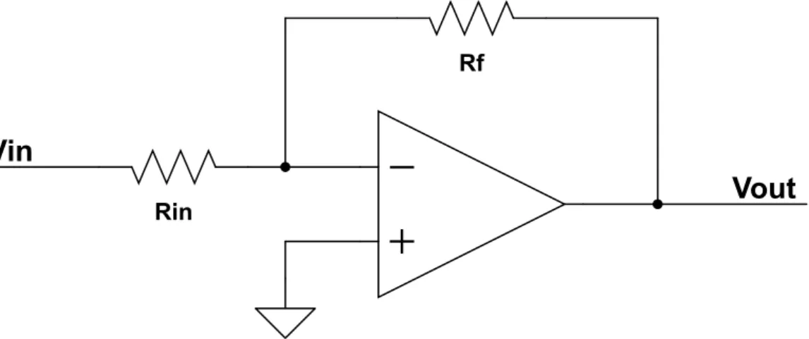
Inverting Amplifier
The inverting amplifiers output voltage changes 180 degrees out of phase
with the input voltage. A typical inverting amplifier is shown in figure 3.12.
Rin
Rf
Vin
Vout
Figure 3.12: An inverting operational amplifier.
If the open-loop gain is very large the gain can approximately be calcu-lated as: A= Vout Vin =−Rf Rin (3.14)
Advantages and Disadvantages
The input impedance in a non-inverting amplifier is very high and is deter-mined by the op-amps input impedance. For an inverting amplifier the input
impedance is Rin as the point where the feedback loop meets the negative
input has zero potential and therefor is virtually ground.
The inverting input can also act as an attenuator by making Rf < Rin,
while the gain of the non-inverting op-amp approaches 1when R1 → ∞.
3.10
Single Supply
Dual supply systems are usually powered by two supplies equal in magnitude, but with reverse polarity. For a voltage powered op-amp the center voltage between the supplies is connected to ground. This makes it possible for any input source connected to ground to be referenced to the center voltage of the supplies and the output voltage is then automatically referenced to ground.
3.10. SINGLE SUPPLY 37
The input and output voltage can normally have values within the power supplies voltage range, both negative and positive.
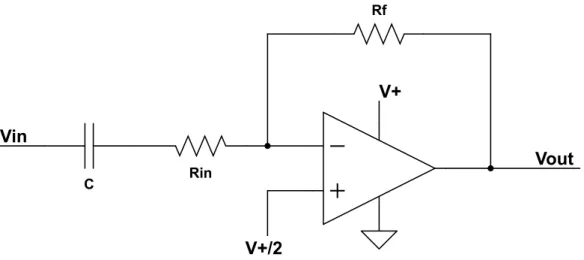
Single supply systems are powered by a single supply and does not have the same ground reference as a dual supply system has. When an input source is connected to ground, it is not referenced to the single supply’s center, but the lower power supply rail, which is ground. This is equivalent to the negative supply in a dual supply system. This means a single supply op-amp is not able to handle negative input signals for a non-inverting amplifier or positive input signals for an inverting amplifier, as it would force the output to go negative, which it cannot. It is therefore necessary to bias the single supply op-amp to avoid this problem. An example of this can be seen in
figure3.13. Rin Rf Vin Vout C V+ V+/2
Figure 3.13: A biased AC coupled inverting operational amplifier. Here the op-amp is biased with half of the op-amps power supply on the positive input. The capacitor on the input assures that only AC voltage is passed through from the input source and vice versa. This circuit superim-poses the passing AC voltage on the bias voltage at the op-amps output, even if the input source signal has positive polarity. The output can only be positive so the input signal amplitude can maximally be half of the sin-gle supply voltage if it is a sine wave centered around zero volt. This also requires that the bias voltage is half the single supply voltage.
As demonstrated, it is possible to use single supply systems to perform the same operations as dual supply systems with some modifications.
The motivation behind using single supply systems is the lower power consumption demands of portable battery-powered devices. Also only one battery is needed.
3.11
Noise in Analog circuits
Noise is present in all analog circuits and three of the most common sources of noise is presented in this section. Noise affects a systems performance and one of the most used parameters to determine the relationship between the signal and noise is the signal-to-noise ratio (SNR). Steps can be taken to reduce noise when the noise source and what type of noise it present in part of a system.
3.11.1
Thermal Noise
The random movement of charge carriers generates thermal noise (also called Johnson noise among other names). Thermal noise is present whether a voltage is applied or not and the more heated the conductor, the more thermal noise will be present. Only at absolute zero degrees is no thermal noise present.
Thermal noise is considered white noise, which means it has a uniform power density in the frequency spectrum.
At frequencies below 100 MHz, thermal noise can be calculated using
Nyquist’s relation (TexasInstruments,2002, c. 10.8):
Eth= √ 4kT RB (3.15) or Ith = Eth R = r 4kT B R (3.16)
where Eth is the thermal noise voltage in Volts rms, Ith is the thermal
noise current in Amps rms,k is the Boltzmann’s constant,T the temperature
in Kelvin,R the resistance in Ohms and B the bandwidth in Hertz.
3.11.2
Shot Noise (Schottky Noise)
Charge carriers are a flow of discrete charges and each time an electron passes a potential barrier noise is generated. This because potential energy is built up until there are enough energy to pass the potential barrier and then released in order for the electrons to pass.
Shot noise is associated with current flowing and there are no shot noise present when there are no current flowing.
Shot noise is also independent of temperature and has a uniform power density in the frequency spectrum.
3.11. NOISE IN ANALOG CIRCUITS 39
Shot noise is mainly present in semiconductors, but also in any conductor due to imperfections and impurities in the metal.
If the semiconductor PN-junction is forward biased the rms shot noise current is:
Ish =
p
2qIdcB (3.17)
where q is the electron charge, Idc is the average forward DC current in
Amperes andB the bandwidth in Hertz.
and the rms shot noise voltage is:
Esh =kT
s
2B qIdc
(3.18)
where k is the Boltzmann’s constant and T the temperature in Kelvin.
Now we can see that the shot noise is inversely proportional to the current. This means that in most conductors shot noise will be very small.
3.11.3
Flicker Noise
Flicker noise (also called 1/f noise) is present in all active and many passive devices. Flicker noise increase with decreasing frequency, hence the name 1/f. Flicker noise is associated with DC current and has the same power
content in each decade (TexasInstruments, 2002, c. 10.8).
The shot noise voltage is:
Ef =KV
s
ln (fmax
fmin
) (3.19)
where KV is a proportionality constant in volts representing Ef at 1 Hz,
fmax and fmin are maximum and minimum frequencies in Hertz.
The shot noise current is:
If =KI
s
ln (fmax
fmin
) (3.20)
where KI is a proportionality constant in amperes representing If at 1
3.12
Transimpedance Amplifier Noise Analysis
There are three main sources of noise in a transimpedance amplifier. The op-amps input voltage noise, its input current noise and the feedback resistors
thermal noise. This section is based on the article by Orozco(2013).
Knowing the transimpedance amplifier’s cut-off frequency from equation
3.8 the equivalent noise bandwidth (ENBW) can be calculated:
ENBW=f−3dB ·
π
2 (3.21)
All noise calculations in this section is root mean square (RMS) values. The feedback resistor’s noise will appear directly on the output as:
NRf =
p
4kT ·ENBW·Rf (3.22)
where k is the Boltzmann constant and T the temperature in Kelvin.
The op-amp’s current noise will appear on the output after going through the feedback resistor as:
Ncurrent =InRf · √
ENBW (3.23)
where In is the current noise density of the op-amp.
With the assumptions that the first pole and zero of the output noise density is minimum a decade lower than the second pole and that the output noise is equal to the plateau noise that is:
N2 =en(
Cf +Csh+Ci Cf
) (3.24)
where en is the voltage noise density,Cf the feedback capacitor, Csh the
shunt capacitance and Ci the op-amps input capacitance.
An estimation of the voltage noise is then:
Nvoltage =N2·
r
π
2fp2 (3.25)
where fp2 is the second pole and defined as:
fp2 =fGBP ·
Cf Cf +Csh+Ci
(3.26)
where fGBP is the gain bandwidth product.
The three noise sources are independent and Gaussian meaning that the total noise is the root-sum-square (RSS):
3.12. TRANSIMPEDANCE AMPLIFIER NOISE ANALYSIS 41
Ntotal =
q
N2
Rf +Ncurrent2 +Nvoltage2 (3.27)
A low pass filter on the transimpedance output can greatly reduce the
Chapter 4
Digital Theory
4.1
ARM
4.1.1
What is ARM
ARM is a family of microprocessors and microcontrollers based on the Re-duced Instruction Set Computer (RISC) architecture. The RISC architecture is often associated with low cost, less heat and low power computer proces-sors. ARM Holdings, which own the ARM family, licenses its chip design and instruction set to third-party companies. Third party companies then add, e.g., memory, peripherals, wireless radios etc. This is what for example ST Microelectronics and Texas Instruments do.
4.1.2
What is ARM Coretex-M3
The ARM Cortex-M3 is one of ARM’s microcontroller cores based on the ARMv7M architecture which is a Harvard architecture with separate code and data busses. It is a bit microcontroller with a mixed 16- and 32-bit instruction set called Thumb2. It is bi-endian, but little endian by de-fault. It supports one clock-cycle hardware multiplication and division and the multiply-and-accumulate (MAC) instruction. The Cortex-M3 is a high-performance low-cost microcontroller widely used in the industry.
4.1.3
Nested Vector Interrupt Controller (NVIC)
Cortex-M3 have an advanced interrupt controller called NVIC. Cortex-M3 can support up to 256 different priority levels and supports both level and
edge interrupts. A higher number corresponds to a lower priority.(ARM,
2010, p. 129) The STM32 only utilize 4 bits for priority levels, which means