warwick.ac.uk/lib-publications
Original citation:
Jahdi, Saeed, Alatise, Olayiwola M., Bonyadi, Roozbeh, Alexakis, Petros, Fisher, Craig A., Ortiz
Gonzalez, Jose Angel, Ran, Li and Mawby, P. A. (Philip A.). (2015) An analysis of the switching
performance and robustness of power MOSFETs body diodes : a technology evaluation. IEEE
Transactions on Power Electronics, Volume 30 (Number 5). pp. 2383-2394.
Permanent WRAP URL:
http://wrap.warwick.ac.uk/69587
Copyright and reuse:
The Warwick Research Archive Portal (WRAP) makes this work by researchers of the
University of Warwick available open access under the following conditions. Copyright ©
and all moral rights to the version of the paper presented here belong to the individual
author(s) and/or other copyright owners. To the extent reasonable and practicable the
material made available in WRAP has been checked for eligibility before being made
available.
Copies of full items can be used for personal research or study, educational, or not-for profit
purposes without prior permission or charge. Provided that the authors, title and full
bibliographic details are credited, a hyperlink and/or URL is given for the original metadata
page and the content is not changed in any way.
Publisher’s statement:
“© 2015 IEEE. Personal use of this material is permitted. Permission from IEEE must be
obtained for all other uses, in any current or future media, including reprinting
/republishing this material for advertising or promotional purposes, creating new collective
works, for resale or redistribution to servers or lists, or reuse of any copyrighted component
of this work in other works.”
A note on versions:
The version presented here may differ from the published version or, version of record, if
you wish to cite this item you are advised to consult the publisher’s version. Please see the
‘permanent WRAP URL’ above for details on accessing the published version and note that
access may require a subscription.
An Analysis of the Switching Performance and
Robustness of Power MOSFETs Body Diodes:
A Technology Evaluation
Saeed Jahdi,
Student Member, IEEE,
Olayiwola Alatise,
Member, IEEE,
Roozbeh Bonyadi,
Student
Member, IEEE,
Petros Alexakis,
Student Member, IEEE,
Craig A. Fisher,
Member, IEEE,
Jose A. Ortiz Gonzalez,
Li Ran,
Senior Member, IEEE,
and Philip Mawby,
Senior Member, IEEE
Abstract—The trade-off between the switching energy and electro-thermal robustness is explored for 1.2kV SiC MOSFET, silicon power MOSFET and 900V CoolMOS body diodes at dif-ferent temperatures. The maximum forward current for dynamic avalanche breakdown is decreased with increasing supply voltage and temperature for all technologies. The CoolMOS exhibited the largest latch-up current followed by the SiC MOSFET and silicon power MOSFET; however when expressed as current density, the SiC MOSFET comes first followed by the CoolMOS and silicon power MOSFET. For the CoolMOS, the alternating p and n pillars of the super-junctions in the drift region suppress BJT latch-up during reverse recovery by minimizing lateral currents and providing low resistance paths for carriers. Hence, the temperature dependence of the latch-up current for CoolMOS was the lowest. The switching energy of the CoolMOS body diode is the largest because of its super-junction architecture which means the drift region have higher doping, hence more reverse charge. In spite of having a higher thermal resistance, the SiC MOSFET has approximately the same latch-up current while exhibiting the lowest switching energy because of the least reverse charge. The silicon power MOSFET exhibits intermediate performance on switching energy with lowest dynamic latching current.
Index Terms—Electro-Thermal Ruggedness, Body Diode, MOSFET, Robustness, Reverse Recovery
I. INTRODUCTION
P
OWER MOSFETs can provide the advantage of fasterswitching compared to IGBTs which use conductivity modulation from minority carrier injection to limit conduction losses. Conventional high voltage silicon power MOSFETs have a considerably high on-state resistance which increases the conduction losses. Hence, their use in power converters is limited to high frequency and low voltage applications. To improve the conduction losses of the high voltage silicon power MOSFETs, the concept of the super-junction was introduced as a way of increasing the blocking voltage without
Manuscript submitted March 31, 2014, revised May 15, 2014; accepted June 26, 2014.
Copyright (c) 2014 IEEE. Personal use of this material is permitted. However, permission to use this material for any other purposes must be obtained from the IEEE by sending a request to [email protected].
This work was supported in part by Science City Research Alliance. The authors are with the Department of Electrical and Electronics of School of Engineering, University of Warwick, United Kingdom E-mail: [email protected] , [email protected] , [email protected] , [email protected], [email protected], [email protected], [email protected] , [email protected]
using thick and highly resistive drift layers. By using alternate n and p pillars in the drift region, lateral as well as vertical depletion resulted in high blocking voltages with less resistive drift layers, hence, the trade-off between blocking voltage and on-state resistance is relaxed [1], [2]. Another avenue through which the performance of the power MOSFET was improved was the transition to wide bandgap semiconductors like SiC where the wider bandgap and higher critical field results in a thinner and less resistive drift layer that can block significantly higher voltages while maintaining a low on-state resistance.
Traditionally, independent discrete diodes are used as re-verse conducting or anti-parallel diodes so as to enable bi-directional power flow. Integral to the design of the MOSFET is the body diode which has the structure of a PiN diode be-cause of the lightly doped voltage blocking drift layer between the n+drain and the p body. The foremost characteristic of PiN diodes is in the turn-off transient where reverse recovery can be observed as a result of minority carrier extraction from the drift layer. As current is ramped down during the turn-off process in the PiN diode, the carrier distribution profile supports the current through the zero crossing until the voltage across
the diode causes depletion widths at the diode PN and NN+
junctions. Once this space charge region forms, the reverse current reaches its peak value (which is the peak reverse recovery current) and then starts to recover to zero. The time it takes for the current to return to zero depends on the rate of minority carrier recombination in the drift region, which in turn is a function of the temperature dependent carrier lifetime amongst other parameters. Although it is generally desirable for the PiN diode to have a minimum reverse recovery time, it can be hazardous if the rate of change of the current with time is very high in the presence of parasitic inductances. PiN diode reverse recovery can be considered to be soft or snappy depending on the ratio between the time taken for the current to change between 0 and the peak reverse current and the time taken to return from that peak reverse current to 0. The voltage across the diode moves from the on-state voltage to the supply voltage although there is usually a peak voltage overshoot due to parasitic inductance and a time varying current. The peak voltage overshoot occurs at the time when the diode is in reverse recovery, hence, snappy diodes can cause high peak
voltages and dV/dt induced avalanche breakdown capable of
the drain-body depletion capacitance, which is proportional to
the dV/dt across the diode. It is also possible for the reverse
recovery current to trigger bipolar latch-up in the device [3]. If sufficient current flows through the body of the MOSFET to increase the potential difference between the p-body and the n-source beyond the built-in diode voltage, the parasitic BJT inherent in the device may latch with destructive consequences [4]. Because the latch-up current has a positive temperature
coefficient, thermal runaway ensues [5]. In SiC MOSFET,
the low minority carrier lifetime in the drift layer coupled with the smaller capacitances means that the switching is faster (dV/dt is higher) and the reverse charge is significantly smaller; whereas in the CoolMOS devices, the alternate p and n doped pillars in the drift region means that the anti-parallel
body diode will be a parallel combination of PN–N+ diodes
and PPN+ diodes. Hence, during reverse recovery, electrons
will be minority carriers in PPN+ diodes whereas holes will
be minority carriers in PN–N+ diodes. Since electrons have
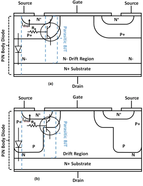
[image:3.612.51.299.381.704.2]higher carrier lifetimes, CoolMOS devices will hence exhibit higher reverse recovery charge which will be made worse by virtue of the fact that the n pillars will be more highly doped since the super-junctions enable high voltage blocking i.e. reverse recovery charge increases with the doping of the drift layer. Figure 1 shows schematic diagrams of a standard power vertically diffused MOSFET and CoolMOS with the inherent body diode and parasitic BJT.
Fig. 1. Cross-sectional schematic of (a) a standard vertical D-MOSFET and (b) a super-junction power MOSFET (CoolMOS) along with the parasitic BJT and the intrinsic diode
To avoid the unintentional use of the PiN body diode, a Schottky diode is normally placed in series with the diode while a further PiN diode is placed as the actual anti-parallel diode [6]–[8]. With the emergence of advanced power devices like Silicon Carbide MOSFETs and CoolMOS superjunction devices, it has become more important to investigate the performance and robustness of the body diodes in switching applications [9], [10]. It has been previously shown that the body diode can be actually be a suitable replacement for the PiN diodes when it comes to soft switching converters such as ZVS [11]–[15]; however, the use of the body diode may create a significant robustness issue when it comes to
hard commutation switching [16]–[18]. To overcome this,
different MOSFET designs were tested including lateral Power
MOSFET [19], [20], VDMOSFT [21], VMOS, LDMOS,
TrenchMOS [22], UMOS [23], semi-super-junction [24] and eventually super-junction MOSFETs [25], [26] or CoolMOS [27] all of which although showed certain improvements, but could not help the overall poor reverse recovery performance of the body diodes during hard commutation. Though certain efforts were made to use methods such as active channel
freewheeling [28] to minimize the effect of the recovery
charge, the performance of the body diode during the reverse recovery could not be improved. Recently developed SiC MOSFETs body diode have reduced the magnitude of the recovery charge [29] which is a considerable step forward, but may also present significant robustness issues [30].
In this paper, the reverse recovery of the body diodes are studied as functions of the switching rate, temperature and for-ward current in silicon power MOSFETs, CoolMOS and SiC MOSFETs. Current is commutated through the free-wheeling diode during a dynamic avalanche breakdown test [31] with incremental forward currents starting from the current rating and moving above the rating so as to investigate the robustness of the device. The experimental measurements are presented in section II and the results of the dynamic avalanche breakdown of the body diode is presented in section III while section IV concludes the paper.
II. EXPERIMENTAL MEASUREMENTS ON BODY DIODES
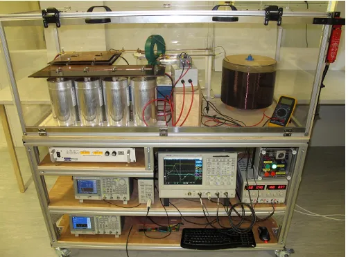
Pearson Electronics wide band current monitor (Model 6656) which is calibrated on a scale of 1 A/V and the voltage is measured using Tektronix (P5210) differential voltage probes scaled on a basis of 1/100. By connecting the gate of the high side transistor to its source, the transistor is an open circuit, hence, only the body diode is active in the circuit. The body diode of the device under test is used to free-wheel current through a pre-charged inductor and a low-side transistor is used to commutate current away from the body diode. Figure 4(a) to (d) shows the different stages of the double pulse test and the direction of current flow in the circuit. When the low side transistor is switched on as shown in the circuit schematic in Figure 4(a), the inductor is charged with a current from the power supply and when it is switched off as shown in Figure 4(b), current commutates from the low side transistor into the body diode of the high side transistor. As the low side transistor is switched on again as shown in Figure 4(c), the body diode of the high side transistor switches off and goes into reverse recovery. As the low side transistor is switched off again in Figure 4(d), current commutates into the body diode where it eventually damps to 0. The duration of the gate pulse of the low side transistor determines the magnitude of the current the body diode will conduct and switch. Both the low and high side transistors for any test are the same technology. As expected the SiC MOSFET has the lowest on-state resistance, followed by CoolMOS and then silicon power MOSFET. The current ratings of the MOSFETs range between 15 and 17 A whereas the voltage ratings are 1.2 kV for the silicon power MOSFET and SiC MOSFET and 900 V for the CoolMOS device (this is the highest voltage rating for a commercially available super-junction MOSFET). Due to the fact that body diodes are not necessarily optimized for the forward current, the initial measurements of the body diode switching performance started from a forward current of 2 A on a gradual increase beyond the current rating until avalanche breakdown was observed. Measurements are performed with a wide range of temperatures between –75°C and 175°C, gate
resistances between 10 Ω and 1000 Ω and forward currents
starting from 2 A to destruction of each body diode, at approximately 40 A at 100 V.
Fig. 2. Schematic of the double pulse circuit and devices under test.
[image:4.612.313.564.56.242.2]Figure 5 show the body diode reverse recovery currents of the silicon power MOSFET when switched with a forward current of 2 A. It should be noted that for a PiN diode, the
[image:4.612.313.561.307.549.2]Fig. 3. The clamped inductive measurement test rig, consisting of a series of bank capacitors, inductors and copper plates to minimize the effect of parasitic inductances.
Fig. 4. The dynamic avalanche breakdown circuit, which is the same as the classic double-pulse quasi switching clamped inductive set up; The forward current is increased by duration of the gate pulse in (a). The turn-off the low side transistor commutates current into the body diode under test in (b). Upon switching in (c), the current commutates to the low-side MOSFET, which causes reverse recovery in the body diode and subjects it to a high
dV/dtwhich may trigger the parasitic BJT to turn on. In (d), the circuit is switched off.
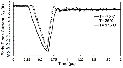
[image:4.612.52.299.547.676.2]the temperature dependent minority carrier lifetime, parasitic inductances as well as forward current. As can be seen from Figure 5, at –75°C and 25°C, increasing the forward current causes the peak reverse recovery current to increase in addition to the stored reverse recovery charge. However at high temperatures (175°C), the increase in the minority carrier lifetime dominates over the effect of forward current, hence, the peak reverse recovery current should remain the same for all forward currents, although the recovery charge is increasing. Temperature also has a significant impact on the body diode as the reverse recovery charge increases with temperature. This is due to the increased minority carrier lifetime in the drift region, hence, lower recombination rates during the recovery phase of charge extraction. The silicon power MOSFET exhibits some oscillations in turn-off when switched at lower temperatures due to the reduced carrier lifetime; hence, a more snappy reverse recovery since the recombination rate is increased. These oscillations are damped as temperature increases and might be a robustness issue because snappy reverse recoveries can induce BJT latch-up from excessive voltage spikes. However, as will be seen in next sections, at higher temperatures, the parasitic BJT in silicon power MOSFETs latches-up at lower forward currents as the temperature is increased. Hence, the impact of temperature on increasing the body resistance and reducing the built in emitter base junction voltage of the parasitic BJT supersedes the effect of lower recombination rate induced by higher temperatures.
Fig. 5. The reverse recovery of the silicon power MOSFET body diode at 2 A at different temperatures. It can be seen that reverse charge increases with temperature and low temperatures can induce snappy recovery.
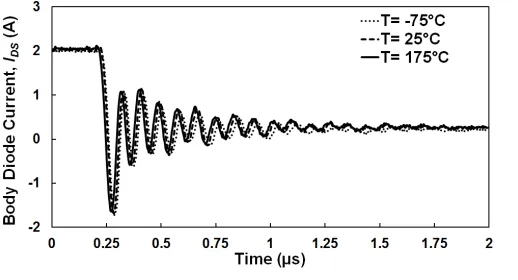
Figure 6 shows the reverse recovery current of the CoolMOS body diode at 2 A forward current. As can be seen, the reverse recovery current is much higher, which is expected since it is a lower voltage rated device and will hence, have a higher drift layer doping. However, it is also thought that the super-junction architecture contributes to the reverse charge firstly by enabling a higher drift layer doping for delivering lower on-state resistance while maintaining a relatively high blocking voltage. Secondly, electrons will also participate as stored charge in the reverse recovery process because of the presence of the p pillars in the n doped drift region. As a result of the fact that electrons have higher carrier lifetimes than holes, there will be higher reverse recovery in CoolMOS compared
[image:5.612.311.563.203.343.2]with silicon power MOSFETs. The impact of temperature on the reverse charge is similar to that in the silicon power MOSFET shown in Figure 5 again as a result of the higher carrier lifetime at higher temperatures. On closer observation, the shape of the reverse current is different in the CoolMOS device compared with the silicon power MOSFET. The slope of the recovery current (positive slope from the peak reverse current to 0) is higher than that of the extraction current (negative slope from 0 to the peak reverse current). This is due to rapid charge extraction in the n and p doped columns in the drift region.
[image:5.612.48.300.396.532.2]Fig. 6. The reverse recovery current of the CoolMOS body diode at 2 A at different temperatures where it can be seen that total reverse charge increases with temperature.
Figure 7 shows the reverse recovery current of the SiC MOSFET body diode switched with a forward current of 2 A.
As can be seen from Figure 7, thedI/dtof the SiC MOSFET
is much higher and temperature has an insignificant effect on the switching characteristics. Also, there is little or no reverse charge and only current oscillations with small amplitudes are evident. What is also interesting to note about the switching characteristics of the SiC MOSFET body diode is the fact that the turn-off characteristics are independent of the forward current thereby indicating that there is little or no charge storage mechanism. This is due to two reasons, firstly the fact that minority carrier lifetime is lower in SiC MOSFET and secondly that the physical area of the die is smaller, hence, there is much smaller area for stored charges. The SiC MOSFET will deliver the most energy efficient switching performance since the switching energy will be the smallest as a result of the fastest transients. The robustness implication of this is investigated in the next section.
Figure 8(a) shows the effect of the gate resistance or the switching rate on the switching characteristics of the body diode for the SiC MOSFET whereas Figure 8(b) and Figure 8(c) show similar characteristics for the silicon power MOSFET and CoolMOS. As expected, increasing the
switch-ing rate increases the dI/dt however also causes increased
Fig. 7. The reverse recovery current of the SiC MOSFET body diode at 2 A at different temperatures where it can be seen that total reverse charge increases with temperature.
is capable of causing parasitic bipolar latch-up. These mea-surements are not destructive because of the low currents and voltages involved, however, increasing the switching rates at higher voltages have destructive consequences. In the case of the CoolMOS device as shown in Figure 8(c), increasing the switching rate does not make the recovery snappier or cause oscillations in the turn-off current. This is due to the fact that the super-junction structure causes a different mechanism of charge extraction from that in the SiC MOSFET and silicon power MOSFETs. This will also account for why the CoolMOS device has the highest latch-up current.
Figure 9(a) shows the body diode switching characteristics of the three technologies at –75°C whereas Figure 9(b) shows similar characteristics at 175°C. Figure 10(a) shows the mea-sured reverse recovery charge as a function of temperature for the 3 technologies where it can be seen that the reverse charge increases with temperature for both the silicon power MOSFETs whereas is temperature invariant for the SiC MOS-FET. Figure 10(b), the reverse charge density is shown as a function of temperature where it can be seen that the silicon power MOSFET and SiC MOSFET have very low reverse charge per unit area compared with the CoolMOS device.
Since current is simply defined as charge flow rate, the total reverse recovery charge can be calculated by the integration of the reverse recovery current over its corresponding transient duration. This integration is done numerically using the reverse recovery waveforms (where the reverse recovery current is negative). The reverse recovery charge density is also the calculated reverse recovery charge per unit area.
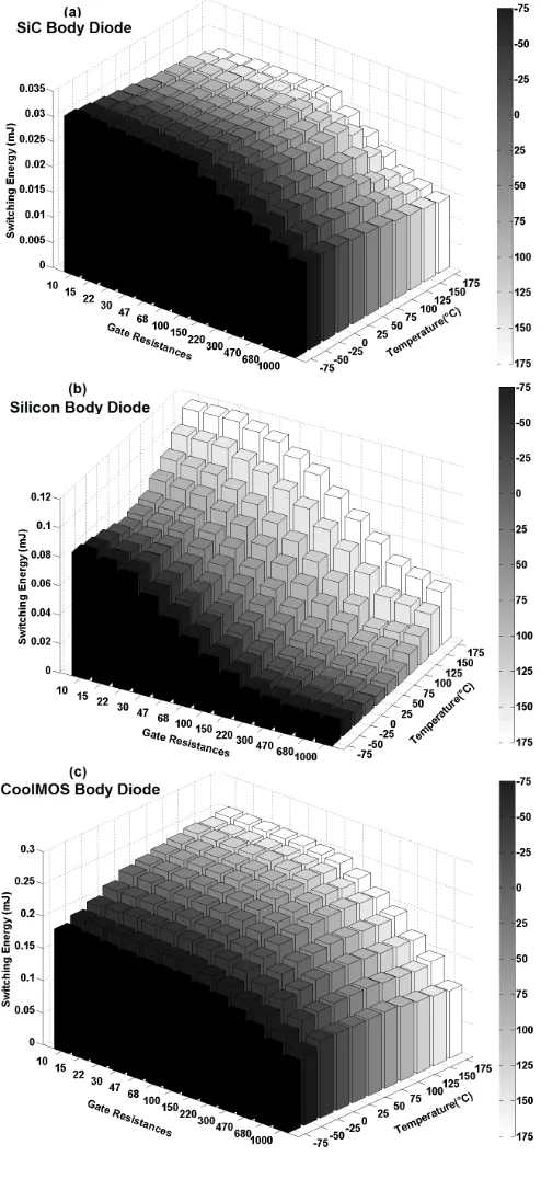
Figure 11(a) shows the body diode switching energy as a function of temperature for the 3 technologies switched
with a gate resistance of 15 Ω whereas Figure 11(b) shows
a similar characteristic for the device switched at 150Ω. The measurements have also been done at different supply voltages so as to ascertain that the trends are repeatable at all voltage levels. Figure 12 shows the calculated body diode switching energy for the 3 technologies as a function of temperature and the switching rate for the (a) SiC MOSFET, (b) the silicon power MOSFET and (c) the CoolMOS. As can be seen, the SiC MOSFET body diode has the least switching energy and
Fig. 8. Reverse recovery current of (a) SiC MOSFET , (b) Silicon Power MOSFET and (c) CoolMOS body diode at 2 A forward current and 100 V supply, showing less oscillations and smaller peak at slower switching rates.
[image:6.612.314.561.58.471.2]Fig. 9. Comparison of the reverse recovery current of SiC MOSFET , Silicon Power MOSFET and CoolMOS body diode with a forward current of 2 A, at (a) –75°C to (b) 175°C showing that CoolMOS body diode has a significantly higher level of the reverse recovery but the least oscillation.
cause faster switching (The RGCGD can be accounted for as
the electrical time constant) thereby resulting in higher peak reverse recovery currents [35]. This peak reverse recovery current coupled with peak voltage overshoot causes significant instantaneous power which increases the switching energy at high switching rates. The increase in switching energy with temperature is due to an in increase carrier lifetime which further increases the reverse recovery charge. This trend is not affected by the magnitude of current and voltage. Therefore, an increase in either the current or voltage will not impact the temperature dependency trend of the switching energy.
III. DYNAMICAVALANCHEBREAKDOWN OFBODY
DIODES
In the converter applications, MOSFETs body diodes may conduct during dead times. SiC MOSFETs have good re-covery performance with low rere-covery charge and signif-icantly faster transients. Additionally, the switching energy of SiC MOSFET body diodes is smaller than discrete PiN diodes, making them a good choice in terms of speed and temperature invariability. However, there are some important robustness considerations [36]. In this section, robustness of the body diode has been studied through a range of dynamic avalanche breakdown tests under hard switching commutation in thermally stressed conditions. The breakdown limits of the technologies are compared under different temperatures, forward current and drain-source voltages. Figure 13 shows how the gate pulse duration can determine the magnitude of
Fig. 10. (a) Body diode reverse recovery charge stored in the body diode as a function of temperature for all 3 technologies with a forward current of 2 A, (b) The reverse recovery charge density as a function of temperature for the 3 technologies.
Fig. 11. The switching energy of the body diodes for all technologies over a wide range of temperatures (–75°C to 175°C ) with the high and low-side MOSFET switching with a gate resistance of (a) RG = 15Ωand (b) RG =
150Ω.
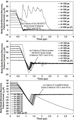
measurements were also performed at different supply voltages for the 3 technologies. The gate resistance used in all the measurements shown in Figure 14 is 10Ω. It is expected that reducing the gate resistance will increase the turn-OFF dV/dt across the body diode, thereby increasing the displacement current of the drain to body depletion capacitance. This will cause a higher voltage drop across the source to body para-sitic resistance which can further trigger body diode failure. Hence switching at faster rates will increase the likelihood of device failure. Very low minority carrier lifetime in Silicon Carbide means that there is minimal recovery charge during turn-OFF. The primary cause of failure in Silicon Carbide
MOSFET body diode is due to highdV/dtin hard commutation
conditions which coupled with high thermal resistance causes high junction temperatures and device failure. The high dV/dt during body diode turn-OFF causes a displacement current which coupled with the body resistance triggers the parasitic BJT. In CoolMOS and silicon Power MOSFET, where the thermal resistance is lower than SiC MOSFET, the high reverse recovery charge and high peak voltage overshoot is the primary cause of failure. This is due to the high instantaneous power where the peak voltage overshoot and peak reverse recovery current coincide. Hence in SiC MOSFET, the device failure is during body diode turn-OFF whereas in silicon Power MOSFET and the CoolMOS , the failure is due to the reverse recovery in body diode.
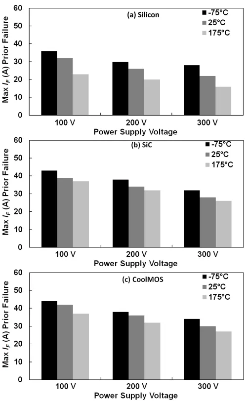
[image:8.612.316.563.57.595.2]Figure 15(a) shows the maximum forward current at differ-ent supply voltages for the 3 technologies at 100 V and 25°C. It can be seen from Figure 15 that the latching current reduces
Fig. 12. The switching energies of body diodes as functions of temperature and switching rate for a constant forward current of 2 A and 100 V for the (a) SiC MOSFET body diode (b) silicon power MOSFET body diode and (c) CoolMOS body diode.
with increasing supply voltage for all technologies. This is
due to the increasingdV/dt anddI/dt with increasing supply
Fig. 13. Pulse length of the lower-side MOSFET’s gate voltage will determine the flowing current with a 450µH inductor.
Fig. 14. Point of Failure in Body diode forward and reverse currents for the body diode of the (a) silicon power MOSFET (fail at 34 A), (b) SiC MOSFET (fail at 42 A) and (c) CoolMOS (fail at 44 A), all at 100 V.
due to the fact that the SiC MOSFET has the smallest active area. At 800 V measurements, the current of the both SiC MOSFET and CoolMOS body diode is around 10 A, even
though the CoolMOS has slightly lower ratings. Figure 16 shows the picture of the physical die sizes which correlates with the thermal resistances and input capacitances stated on the datasheet. The SiC MOSFET device clearly has the smallest die area which is responsible for its high thermal resistance. This means that the device has a smaller thermal mass which results in higher temperature excursions. Hence, the current density is the critical parameter in determining BJT latch-up during the turn-off transient in the body diode since the higher temperature further increases the body resistance. BJT latch-up depends on the combination of a high source-body resistance and a high source-source-body current both of which combine to cause a voltage sufficient to forward bias the parasitic BJT.
Fig. 15. (a) The latch up current as a function of supply voltage for the 3 technologies at 25 °C. (b) The latch-up current density as a function of supply voltage for the 3 technologies at 25 °C.
[image:9.612.50.301.247.645.2] [image:9.612.316.562.578.700.2]The impact of temperature on the latch-up current for different voltages is plotted in Figure 17(a), 17(b) and 17(c) respectively for silicon power MOSFET, SiC MOSFET and the CoolMOS body diodes. It can be seen from these figures that increasing the temperature reduces the latch-up current for the silicon power MOSFET and SiC MOSFET. In the case of the CoolMOS device, when the body diode is in the forward conductive mode, a finite amount of charge is stored in the N-drift region of the diode/MOSFET. During the reverse
recovery of the body diode, the displacement current induced during the formation of the depletion layer in the PN-junction can constitute the base current of the parasitic BJT. Parasitic BJT latch-up thus occurs if the p-well resistance and base current are large enough to provide a base-emitter voltage larger than the built-in voltage of the BJT. The charging current of the depletion capacitance is the product of the capacitance
and the dV/dt across the diode. Hence, BJT latch-up has a
higher probability during fast switching when dV/dt is high.
The temperature dependence of dV/dt has been determined
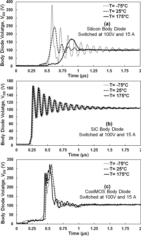
through measurements and is shown in Figure 18(a) for the silicon power MOSFET, Figure 18(b) for the SiC MOSFET and Figure 18(c) for the CoolMOS body diodes when switched with a 100 V supply.
It can be seen from Figure 18(a) that dV/dt decreases as
temperature increases in silicon power MOSFET. At –75°C, there is significant voltage overshoot across the diode with oscillations. This correlates with Figure 5 where the snappiness of the reverse recovery characteristics can be seen to increase as temperature reduces for the silicon power MOSFET. The
reason for the increasing dV/dt with reduced temperatures is
the carrier lifetime dependence on temperature. It is known from the physics of PiN diodes that the voltage across the diode starts rising at the point when the minority carriers have been extracted from the drift region via a negative current. At this point, the charge density in the diode can no longer support the current through it and electric fields start to form at the P+N- and N+N- junctions thereby depleting them of
carriers. As this occurs, the remaining charges in the drift region recombine at a rate that depends on the minority carrier lifetime. At low temperatures, where the lifetime is reduced, the tail current in the reverse recovery characteristic is snappy and can cause oscillations. At high temperatures, where the lifetime is high, there is a long tail current. This is evident in Figure 5 for the silicon power MOSFET. However, the BJT latch-up also depends on the resistance of the p-body which increases with temperature. Hence, as the temperature
is increased, although dV/dt reduces (which in the one hand
will make BJT latch-up less probable), the p-body resistance increases (which makes BJT latch-up more probable). Hence, the conclusion from the measurements in Figure 18(a) is that the positive temperature coefficient of the p-body resistance is the primary determinant of the temperature dependence of BJT latch-up. Figure 18(b) shows that dependence of the body
diode dV/dton temperature in SiC MOSFET is small enough
[image:10.612.313.562.52.458.2]for it to be considered temperature invariant. This correlates with the body diode turn-off currents presented in Figure 7 which were also temperature invariant. Again, this is as a result of the significantly smaller minority carrier lifetime in
Fig. 17. Maximum latch-up current shown as a function of supply voltage at –75°C, 25°C and 175°C for (a) silicon power MOSFET, (b) SiC MOSFET and (c) CoolMOS body diodes.
SiC, hence, the dependence of the turn-off characteristics on temperature is negligible. However, the dependence of the latch-up current on temperature is more evident as shown in Figure 17(b). This is due to the temperature dependence of the p-body resistance which increases with temperature thereby forward biasing the parasitic BJT. Figure 18(c) shows that
the dV/dt characteristic of the CoolMOS body diode is also
in the p-well is reduced and consequently the possibility of triggering the parasitic BJT is also reduced.
Fig. 18. The turn-off voltage transients of the (a) SiC MOSFET, (b) silicon power MOSFET, and (c) CoolMOS body diode at different temperatures showing increasing dV/dt as the temperature is reduced in silicon power MOSFET while it is temperature invariant is SiC MOSFET and CoolMOS.
Figure 19(a) and Figure 19(b) show the voltage and current transient characteristics of the three body diode technologies switched at 25°C and RG= 10Ω. It can be seen from Figure 19
that the devices have approximately the same dV/dt, hence,
differences between the dV/dt cannot be attributed to the
differences in latching current. In the case of the CoolMOS, the higher forward latching current compared to silicon power MOSFET is due to the effect of the superjunction architecture on the suppression of lateral current flow needed to trigger the parasitic BJT. In the case of the SiC MOSFET, the higher forward latching current is due to the lower instantaneous switching power resulting from insignificant reverse recovery charge (this is in spite of having a larger thermal resistance than the silicon power MOSFET). Figure 19(b) shows the re-verse recovery characteristics of the three technologies at 800
V with a forward current of 5 A. Again, the CoolMOS device has the largest reverse charge while the SiC MOSFET has the smallest. The highest switching energy of the CoolMOS device does not affect its immunity to BJT latch-up negatively because of the super-junction architecture which suppresses lateral currents during reverse recovery [37].
Fig. 19. The 800 V measurements showing body diode’s (a) voltage and (b) current of the three technologies.
IV. CONCLUSION
[image:11.612.318.563.139.418.2]the CoolMOS and SiC MOSFETs had the highest latch-up current followed by the silicon power MOSFET. Furthermore, the SiC MOSFET showed the highest latch-up current density (since it has the smallest die area) followed by the CoolMOS and the silicon power MOSFET.
REFERENCES
[1] L. Lorenz, G. Deboy, and I. Zverev, “Matched pair of coolmos transistor with sic-schottky diode - advantages in application,”Industry Applica-tions, IEEE Transactions on, vol. 40, no. 5, pp. 1265–1272, Sept 2004. [2] J. Zhang and J.-S. Lai, “A synchronous rectification featured soft-switching inverter using coolmos,” inApplied Power Electronics Conf. and Expo., APEC ’06. 21st Annual IEEE, March 2006, p. 6. [3] H. Yilmaz, K. Owyang, P. O. Shafer, and C. Borman, “Optimization
of power mosfet body diode for speed and ruggedness,” Industry Applications, IEEE Transactions on, vol. 26, no. 4, pp. 793–7, Jul 1990. [4] B. Pejcinovic and et al., “Role of parasitic bjt in the design of dmosfet,”
inComputers in Power Electronics, IEEE, Aug 1996, pp. 128–31. [5] F. Iannuzzo and et al., “Measurement of the bjt activation current during
the reverse recovery of power mosfet’s drain-source diode,”IEEE Trans. Elec. Devi., vol. 48, no. 2, pp. 391–3, Feb 2001.
[6] L. Mweene, C. Wright, and M. Schlecht, “A 1 kw 500 khz front-end converter for a distributed power supply system,”Power Electronics, IEEE Transactions on, vol. 6, no. 3, pp. 398–407, Jul 1991.
[7] A. Brambilla, E. Dallago, P. Nora, and G. Sassone, “Study and imple-mentation of a low conduction loss zero-current resonant switch,”IEEE Trans. Indus. Electr., vol. 41, no. 2, pp. 241–250, Apr 1994.
[8] D. e. a. DeWitt, “The pinch-off circuit: Reducing noise and component stresses by eliminating body diode conduction in synchronous rectifiers,” inAppl. Pow. Elec. Conf., APEC 22nd, Feb 2007, pp. 1531–36. [9] L. Saro, K. Dierberger, and R. Redl, “High-voltage mosfet behavior
in soft-switching converters: analysis and reliability improvements,” in
Telecom. Energy Conf., INTELEC, 20th Inter., 1998, pp. 30–40. [10] J. Zeng and et al., “Optimization of the body-diode of power mosfets
for high efficiency synchronous rectification,” inPower Semiconductor Devices and ICs, 12th Inter. Symposium, 2000, pp. 145–48.
[11] H. Yu, X. Huang, and J.-S. Lai, “A novel load adaptive zero voltage switching utilizing diode reverse recovery current for soft-switching choppers,” inIndustry Applications Conf., 26th IAS Annual Meeting, IEEE, vol. 3, Sept 2001, pp. 1845–1850 vol.3.
[12] K. Shenai, P. Singh, S. Rao, D. Sorenson, K. Chu, and G. Gaylon, “On the reliability of dc-dc power converters,” inEnergy Conversion Engineering Conf., IECEC 35th, vol. 2, 2000, pp. 1480–1490 vol.2. [13] J. Zhou, M. Xu, J. Sun, and F. Lee, “A self-driven soft-switching
voltage regulator for future microprocessors,”Power Electronics, IEEE Transactions on, vol. 20, no. 4, pp. 806–814, July 2005.
[14] Y. Ren, M. Xu, J. Sun, and F. Lee, “A family of high power density unregulated bus converters,”Power Electronics, IEEE Transactions on, vol. 20, no. 5, pp. 1045–1054, Sept 2005.
[15] H. Mao, S. Deng, J. Abu-Qahouq, and I. Batarseh, “Active-clamp snubbers for isolated half-bridge dc-dc converters,”Power Electronics, IEEE Transactions on, vol. 20, no. 6, pp. 1294–1302, Nov 2005. [16] K. Shenai, P. Singh, S. Rao, D. Sorenson, K. Chu, and G. Gaylon,
“Power supply design for performance and reliability,” in National Aerospace and Electronics Conference, 2000. NAECON 2000. Proceed-ings of the IEEE 2000, 2000, pp. 524–531.
[17] S. Ye, W. Eberle, and Y.-F. Liu, “A novel non-isolated full bridge topology for vrm applications,”Power Electronics, IEEE Transactions on, vol. 23, no. 1, pp. 427–437, Jan 2008.
[18] H. Mao, O. Abdel Rahman, and I. Batarseh, “Zero-voltage-switching dc-dc converters with synchronous rectifiers,”Power Electronics, IEEE Transactions on, vol. 23, no. 1, pp. 369–378, Jan 2008.
[19] A. Testa, S. De Caro, and S. Russo, “A reliability model for power mos-fets working in avalanche mode based on an experimental temperature distribution analysis,”Power Electronics, IEEE Transactions on, vol. 27, no. 6, pp. 3093–3100, June 2012.
[20] Y. Xiong, H. Jia, W. Deschaine, S. Sun, X. Cheng, G. Dashney, D. Okada, and Z. Shen, “Optimization of body diode reverse recovery characteristics of lateral power mosfets for synchronous rectifier dc-dc converters,” inPower Semiconductor Devices and IC’s, ISPSD, 20th Inter. Symp., May 2008, pp. 99–102.
[21] X. Cheng, J. Sin, B. Kang, C. Feng, Y. Wu, and X. Liu, “Fast reverse recovery body diode in high-voltage vdmosfet using cell-distributed schottky contacts,”Electron Devices, IEEE Transactions on, vol. 50, no. 5, pp. 1422–1425, May 2003.
[22] T. Lopez, R. Elferich, and N. Koper, “Reverse recovery in high density trench mosfets with regard to the body-effect,” inPower Semiconductor Devices and IC’s, ISPSD IEEE Inter. Sympo., June 2006, pp. 1–4. [23] Y.-C. Liang, R. Oruganti, and T. Oh, “Design optimisation of power
mosfet for high frequency synchronous rectification,” in Industrial Electronics, Control, and Instrumentation, 1993. Proceedings of the IECON ’93., International Conference on, Nov 1993, pp. 767–772 vol.2. [24] W. Saito and et al., “High breakdown voltage (1000 v) semi-superjunction mosfets using 600-v class semi-superjunction mosfet process,”
IEEE Trans. Electr. Devic., vol. 52, no. 10, pp. 2317–22, Oct 2005. [25] W. Saito, I. Omura, S. Aida, S. Koduki, M. Izumisawa, and T. Ogura,
“Semisuperjunction mosfets: new design concept for lower on-resistance and softer reverse-recovery body diode,”Electron Devices, IEEE Trans-actions on, vol. 50, no. 8, pp. 1801–1806, Aug 2003.
[26] J. Roig, E. Stefanov, and F. Morancho, “Thermal behavior of a super-junction mosfet in a high-current conduction,”Electron Devices, IEEE Transactions on, vol. 53, no. 7, pp. 1712–1720, July 2006.
[27] R. Burra and K. Shenai, “Coolmos integral diode: a simple analytical reverse recovery model,” in Power Electronics Specialist Conference, PESC’03., IEEE 34th Annual, vol. 2, June 2003, pp. 834–838 vol.2. [28] H. Kim, T. Jahns, and G. Venkataramanan, “Minimization of reverse
re-covery effects in hard-switched inverters using coolmos power switches,” inIndus. Applic. Conf., 36th IAS IEEE, vol. 1, Sept 2001, pp. 641–7. [29] P. Losee, K. Matocha, S. Arthur, J. Nasadoski, Z. Stum, J. Garrett,
M. Schutten, G. Dunne, and L. Stevanovic, “Dc and transient per-formance of 4h-sic double-implant mosfets,” Electron Devices, IEEE Transactions on, vol. 55, no. 8, pp. 1824–1829, Aug 2008.
[30] L. Yu and et al., “Reliability issues of sic mosfets: A technology for high-temperature environments,”Device and Materials Reliability, IEEE Transactions on, vol. 10, no. 4, pp. 418–426, Dec 2010.
[31] J. Chen, L. Radic, and T. Henson, “Suppressing channel-conduction dur-ing dynamic avalanche to improve high density power mosfet ruggedness and reverse recovery softness,” inPower Semiconductor Devices and ICs (ISPSD), 25th International Symposium on, May 2013, pp. 321–324. [32] O. Alatise, N.-A. Parker-Allotey, D. Hamilton, and P. Mawby, “The
impact of parasitic inductance on the performance of silicon carbide schottky barrier diodes,” Power Electronics, IEEE Transactions on, vol. 27, no. 8, pp. 3826–3833, Aug 2012.
[33] S. Jahdi, O. Alatise, C. Fisher, L. Ran, and P. Mawby, “An evaluation of silicon carbide unipolar technologies for electric vehicle drive-trains,”
Emerging and Selected Topics in Power Electronics, IEEE Journal of, vol. 2, no. 3, pp. 1–12, June 2014.
[34] C. A. Fisher and et al., “Improved performance of 4h-sic pin diodes using a novel combined high temperature oxidation and annealing process,”Semiconductor Manufacturing, IEEE Transactions on, vol. PP, no. 99, pp. 1–8, July 2014.
[35] Y. Wang, Q. Zhang, J. Ying, and C. Sun, “Prediction of pin diode reverse recovery,” inPower Electronics Specialists Conference, 2004. PESC 04. 2004 IEEE 35th Annual, vol. 4, 2004, pp. 2956–2959 Vol.4.
[36] H. Wang and et al., “Transitioning to physics-of-failure as a reliability driver in power electronics,” Emerging and Selected Topics in Power Electronics, IEEE Journal of, vol. 2, no. 1, pp. 97–114, March 2014. [37] R. Mente, “500v superjunction mosfet for consumer and lighting
appli-cations,”500V CoolMOSTM CE, vol. AN 2012-04, p. 11, April 2012.
Saeed Jahdi (S’10) received the BSc degree in
Olayiwola Alatise(M’05) received the B.Eng. de-gree (with first-class honors) in electronic engineer-ing and the Ph.D. degree in microelectronics and semiconductors from Newcastle University, U.K., in 2008. His research focused on mixed-signal per-formance enhancements in strained Si/SiGe met-aloxidesemiconductor field-effect transistors (MOS-FETs). In June 2008, he joined the Innovation R&D Department, NXP Semiconductors, as a Develop-ment Engineer, where he designed, processed, and qualified discrete power trench MOSFETs for auto-motive applications and switched-mode power supplies. In November 2010, he became a Science City Research Fellow with the University of Warwick and since August 2012, he is serving as assistant professor of Electrical Engineering in University of Warwick, Coventry, U.K. His research interest include investigating advanced power semiconductor materials and devices for improved energy conversion efficiency.
Roozbeh Bonyadi (S’14) graduated his 1st class
BSc honours degree in Electrical-Electronics En-gineering from Shahed University of Tehran. Fol-lowing this, he came to England to undertake his MSc degree, graduating with a Merit in Electronic Systems at the University of Warwick, UK. His MSc project was intelligent fault diagnosis in automotive electronic systems of systems of premium vehicles in collaboration with Jaguar Land Rover PLC. After his graduation he started working as a KTP associate at the University of Wolverhampton in collaboration with Phoenix Calibration & Services Ltd. His interest in hybrid/electric vehicles and semiconductor devices and power module packaging led him to undertake a PhD in Power Electronics at the University of Warwick. His PhD project is sponsored by EPSRC in collaboration with Jaguar Land Rover. He is a member of the IEEE, IAS, and PELS.
Petros Alexakis(S’12) received the BSc degree in
Physics from Aristotle University of Thessaloniki in 2010 with a major in Electronics and Telecommuni-cations and the MSc degree with merit in Renewable Energy and Power Electronics from the School of Engineering of University of Warwick in 2012. He also worked as a private tutor teaching Physics and Math as well as an Electrical Engineer in the Greek Navy. He is currently pursuing his Ph.D. in electrical engineering and more specifically in wide bandgap semiconductor devices in PEATER group in the School of Engineering of University of Warwick. He has been awarded an EPSRC scholarship for the duration of his research. His current research interests include modelling of wide band-gap semiconductor devices, reliability and ruggedness. Mr. Alexakis is a student member of IEEE.
Craig A. Fisher(S’11) was born in Warwickshire,
UK, in 1984. He received the M.Sc. degree in Advanced Electronics Engineering in 2010, and the Ph.D degree in the field of silicon carbide power electronics in 2014, both from the University of War-wick. His Ph.D was funded by the EPSRC HubNet project, and was focused on three principle areas: novel edge termination solutions for high voltage power devices, carrier lifetime enhancement using high temperature processes and the formation of robust ohmic contacts to p-type 4H-SiC. Dr. Fisher currently works as a Research Fellow within the School of Engineering at the University of Warwick, on the EPSRC Underpinning Power Electronics project. His research interests include modelling of 4H-SiC power devices, and the fabrication and characterisation of 4H-SiC devices for high voltage (>10 kV) and high temperature (>300◦C) applications.
Jose Angel Ortiz Gonzalez received a degree in
Electrical Engineering in 2009 from the University of Vigo, Vigo, Spain. From 2010 to 2012 he worked as a Support Technician at the Department of Elec-tronics Technology, University of Vigo, Spain. Since 2013 he has been working at the School of Engi-neering, University of Warwick, Coventry, United Kingdom as a Senior Power Electronics Research Technician currently focusing on high voltage silicon carbide based DC-DC and DC-AC power converters. His current research interests include power convert-ers, circuit testing and device evaluation.
Li Ran (M’98-SM’07) received a PhD degree in
Power Systems Engineering from Chongqing Uni-versity, Chongqing, China, in 1989. He was a Research Associate with the Universities of Ab-erdeen, Nottingham and Heriot-Watt, at AbAb-erdeen, Nottingham and Edinburgh in the UK respectively. He became a Lecturer in Power Electronics with Northumbria University, Newcastle upon Tyne, the UK in 1999 and was seconded to Alstom Power Conversion, Kidsgrove, UK in 2001. Between 2003 and 2012, he was with Durham University, UK. He joined the University of Warwick, Coventry, UK as a Professor in Power Electronics - Systems in 2012. His research interests include the application of Power Electronics for electric power generation, delivery and utilisation.
Philip Mawby (S’85-M’86-SM’01) received the
B.Sc. and Ph.D. degrees in electronic and electrical engineering from the University of Leeds, U.K., in 1983 and 1987, respectively. His Ph.D. was focused on GaAs/AlGaAs heterojunction bipolar transistors for high-power radio frequency applications at the GEC Hirst Research Centre, Wembley, U.K.
In 2005, he joined the University of Warwick, Coventry, U.K., as the Chair of power electronics. He was also with the University of Wales, Swansea, U.K. for 19 years and held the Royal Academy of Engineering Chair for power electronics, where he established the Power Electronics Design Center. He has been internationally recognized in the area of power electronics and power device research. He was also involved in the development of device simulation algorithms, as well as optoelectronic and quantum-based device structures. He has authored or coauthored more than 100 journal and conference papers. His current research interests include materials for new power devices, modeling of power devices and circuits.