C-Cube Microsystems
ii C-Cube Microsystems
C-Cube Microsystems reserves the right to change any products described herein at any time and without notice. C-Cube Microsystems assumes no responsibility or liability arising from the use of .the prod-ucts described herein, except as expressly agreed to in writing by C-Cube Microsystems. The use and purchase of this product does not convey a license under any patent rights, copyrights, trademark rights, or any other intellectual property rights of C-Cube Microsystems. Trademark Acknowledgment:
C-Cube, CL550, and CL560 are trademarks of C-Cube Microsystems. The corporate logo is a registered trademark of C-Cube Microsystems. Windows and Video-for-Windows are trademarks of Microsoft Corpo-ration. Apple and Apple QuickTime are trademarks of Apple Computer, Inc.
© C-Cube Microsystems 1993 All rights reserved
C-Cube Microsystems 1778 McCarthy Boulevard
Milpitas, CA 95035 Telephone (408) 944-6300
Fax (408) 944-6314
Customer Comments and Feedback:
If you have comments about this document, send them to the C-Cube Technical Publications Department at the address listed above, or send e-mail to:
This manual is the primary users guide for the C-Cube CL550 and CL560 JPEG Compression Processors. It contains detailed information about the CL550 and CL560 hardware and also provides general infor-mation on how to program the parts.
This manual is intended for:
D System designers and managers who are evaluating the CL550 and CL560 for possible use in a system
D Designers and hardware engineers who are designing a system based on the CL550 and CL560
D Programmers and software engineers who are writing application programs that interact with the CL550 and CL560
This manual is divided into these chapters:
D Chapter 1, Introduction, presents an introduction to the architec-ture of the CL550 and CL560
Audience
the external signals on the CL550 and CL560.
o Chapters 4 and 5, Host Interface and Video Interface, present functional descritions for the main interfaces of the CL550 and CL560.
o Chapter 6, Specifications, includes detailed electrical and me-chanical specifications.
o Chapter 7, Registers, describes in detail each of the internal regis-ters of the CL550 and CL560.
o Chapter 8, System Designer's Guide, provides a general overview on programming the CL550 and CL560 with initialization proce-dures and compression/decompression procedure flowcharts.
Conventions
Please note the following conventions that are used in this manual: o Hexadecimal numbers are indicated by the prefix Ox, for example,OxFF. Binary numbers are indicated by a subscript, for example, 102. Otherwise, all numbers used in this guide are decimal num-bers unless otherwise noted.
Revision History
This manual, part # 90-1556-101 Rev A., supersedes the previous revi-sion by the same name. The major content changes include:iv C-Cube Microsystems
o Chapter 6, Specifications: AC timing parameters are listed for 7 products and speed grades:
o CPGA package (3): CL550-35, CL550-30, CL560-30 o MQUAD package (4): CL550-10, CL550-30, CL560-15~
CL560-30
1
Introduction
1.1 Cl550 Features 1-2
1.2 Cl560 Improvements 1-2
1.3 Applications 1-3
1.4 Product Family 1-3
1.5 Cl550 Functional Description 1-4
1.6 Cl560 Functional Description 1-6
2 JPEG Overview
2.1 JPEG Background Information 2-2 2.2 Operation of the JPEG Algorithm 2-3
2.3 Discrete Cosine Transform 2-4
2.4 Quantization 2-5
2.5 Zero Run-length Coding 2-7
2.6 Entropy Encoding 2-8
2.7 Summary of JPEG Baseline 2-8
3 Signal Descriptions
3.1 Host Interface 3-3
3.1.1 Data Transfer Signals 3-3
vi C-Cube Microsystems
3.1.2 DMA Signals
mm
DMA_MSTR 3.1.3 Interrupt SignalsNf\ifRTI HALF_FULL
fRTI1
IRQ2
3.1.4 Timing and Control Signals START
TMO
nvrr
TM2
TMoUT FRMEND HBCLK RESETTEST
3.2 Video Interface3.2.1 Pixel Data, Address and Handshake Signals PXDA T[23:0] PXADR[15:0] PXRE PXWE PXIN
PXOUT
STALL3.2.2 Video Synchronization Signals HSYNC
VSYNC BLANK
3.2.3 Video Clock Signals PXCLK
PXPHASE ClK3
4 Host Interface
4.1 Register Access Timing 4.1.1 Signal Descriptions
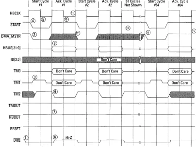
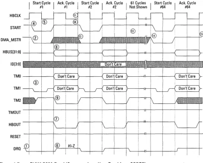
4.2 DMA Access Timing 4-12
4.2.1 CL560 DMA Transfers 4-14
4.2.2 CL560 DMA Write Transaction Timing 4-15 4.2.3 CL560 DMA Read Transaction Timing 4-17 4.2.4 Alternative Method of CL550/560 DMA Transfers 4-19 4.2.5 CL550 Burst-mode Write Transaction Timing 4-20 4.2.6 CL550 Burst-mode Read Transaction Timing 4-22 4.2.7 Operational Considerations 4-23
4.3 Control Signals 4-25
4.3.1 RESET 4-25
4.3.2 NMRn: 4-26
4.3.3 HALF_FULL 4-26
4.3.4 TROJ,IRQ2 4-26
5 Video Interface
5.1 Overview 5-2
5.1.1 Signal Descriptions 5-3
5.1.2 Video Interface Clocks 5-4
5.1.3 Master/Slave Mode Operation 5-7
5.1.4
STArr
Operation 5-75.2 Video Interface Logic 5-10
5.2.1 Pixel Order Conversion 5-10
5.2.2 Window Management and Control 5-12
5.2.3 Color Conversion 5-12
5.3 Basic System Configurations 5-14
5.4 Timing Diagrams Compression Mode 5-17 5.5 Timing Diagrams Decompression Mode 5-29
6 Specifications
6.1 Operating Conditions 6-2
6.2 AC Characteristics 6-3
6.2.1 Host Interface Control Signal Timing 6-4 6.2.2 Video Interface Signal Timing 6-16
6.3 Package Specifications 6-23
6.3.1 144-Pin Ceramic Pin-Grid Array 6-24
6.3.2 144-Pin MQUAD Package 6-29
7 Registers
7.1 Video Interface Registers 7-6
VPeriod Register 7-9
VSync Register 7-10
VDelay Register 7-10
VActive Register 7-11
Video Latency Register 7-11
Vertical Line Count Register 7-12
H Control Register 7 -12
VControl Register 7-12
HV Enable Register 7-13
Color Transformation Matrix 7-13
DCTTabies 7-15
7.2 Compression and Decompression Registers 7-15
Quantizer Tables 7-15
Quantizer A/B Table Select Register 7-16 Quantizer VIC Table Sequence Register 7-17 Quantizer A/B Table Sequence Register 7-18
Quantizer Sync Register 7-18
Coder/Decoder DPCM Reg. Seq. Registers, RH 7-19 Coder/Decoder DPCM Reg. Seq. Registers, RL 7-19 Decoder DPCM Reset Register 7-20
Huffman Code Tables 7-20
Huffman Table Load Enable Register 7-20 Huffman Table Sequence Register 7-21 Coder Attributes Register 7-21 Coder Coding Interval Registers 7-22 Coder Sync Register(CL560) .7-22 Compressed Word Count Register, High (Cl560) 7-23 Compressed Word Count Register, Low (CL560) 7-23 Coder Rate Control Active Register(CL560) 7-24 Coder Rate Control Enable Register (CL560) 7-24 Coder Robustness Active Register (CL560) 7-25 Coder RST Padding Control Register (Cl560) 7-25
Start of Frame Register 7-26
Decoder Table Sequence length Register 7-26
Decoder Marker Register 7-26
Decoder Resume Flag (Cl550) 7-26 Decoder Code Order Register 7-27 Decoder Start Register (CL560) 7-27 Decoding Mismatch Register (Cl560) 7-27
Start Register 7-29
Version Register 7-30
Init Registers 7-30
Flags Register 7-31
1\fM1m Interrupt Mask Register (CL550) 7-33
rm:rr
Mask Register (CL560) 7-34DMA Request Interrupt Mask Register 7-35 IRQ2 Interrupt Mask Register (CL560) 7-37 fRMENo Enable Register (CL560) 7-38
CODEC Register (CL550) 7-39
CODEC FIFO (CL560) 7-40
FIFO Level Register (CL560) 7-40 8 System Designer's Guide
8.1 Typical System Configurations 8-1
8.2 JPEG Video Concepts 8-4
8.3 CL550 Compression Operation 8-5
8.3.1 Overview 8-5
8.3.2 CL550 Operation as a Still-image Coprocessor 8-7 8.3.3 Operation as a Video Compression Processor 8-10 8.3.4 Use of DMA and Interrupts with the CL550 8-12 8.3.5 DMA System Programming Example 8-14
8.4 CL560 Compression Operation 8-16
8.4.1 CL560 Enhancements 8-16
8.4.2 CL560 Operational Differences from the CL550 8-18 8.4.3 Compressed Data Rate Control Mechanisms 8-19 8.4.4 Typical Compression System Using the CL560 8-21 8.4.5 Slave-mode Compression Operation 8-23 8.5 CL550 Decompression Operation 8-25
8.5.1 Overview 8-25
8.6 CL560 Decompression Operations 8-28 8.7 CL5xx Initialization Procedures 8-30
8.7.1 Overview 8-30
8.7.2 Programming the Video Interface Control Registers 8-32 8.7.3 HControl, VControl Registers Programming 8-34
8.7.4 DCT Lookup Table 8-35
8.7.11 CL5xx Start-up Sequence 8-37 8.7.12 Device Reset Considerations 8-38 8.8 Programming the Huffman Tables 8-41
8.8.1 Extracting Huffman Tables from ISO JPEG
Interchange Format 8-41
8.8.2 CL550 Huffman Table Formats 8-41 8.8.3 CL560 Huffman Table Format 8-47 8.9 CL5xx Quantizer Table Programming 8-50
8.9.1 Overview 8-50
8.9.2 Q Table Scaling Function 8-51 8.9.3 Generating Machine-Loadable Q Tables for CL5xx Devices 8-53
8.10 Custom Block Sequencing 8-56
8.10.1 Restrictions 8-56
8.10.2 CL5xx Internal Component Sequencing 8-56 8.10.3 CL550 Component Sequence Programming 8-57
1-1 CL550 Block Diagram 1-4
1-2 CL560 Block Diagram 1-6
2-1 Basic Image Compression Scheme for Coder and Decoder 2-3 2-2 Quantizer Stepping (Uniform Quantization) 2-5 2-3 Psychovisual Weighting Functions for the Luminance and
Chrominance Components 2-6
2-4 Zigzag Pattern for Reordering the 8 x 8 DCT Coefficients 2-7 3-1 CL550 and CL560 Logic Diagrams 3-2
3-2 Strip Buffer RAM Connections 3-9
4-1 CL550 and CL560 Host Interface Block Diagram 4-2 4-2 10[3:0] Chip Select Address Format 4-4
4-3 Register Read Transa ction 4-10
4-4 Register Write Transaction 4-11
4-5 DMA Mode Operation 4-13
5-6 Video Field Descriptions 5-13 5-8 Typical Video System Application 5-14 5-7 RGB to YUV Conversion Operation 5-14 5-9 Typical Still-frame Application 5-15 5-10 Typical Multimedia System Application 5-16 5-11 Typical CL560 Synchronous Interface 5-18
5-12 Compression Overview 5-19
5-13 First Active Line (Compression) 5-22 5-14 Beginning of First Active Line with Active PXRE (Compression) 5-24 5-15 Last Line with Active PXIN (Compression) 5-26 5-16 Last Line with Active PXRE (Compression) 5-28
5-17 Decompression Overview 5-30
5-18 First Line with Active PXWE (Decompression) 5-32 5-19 First Active Line with Active PXOUT 5-34
5-20 Last ActiveLine with PXWE 5-36
5-21 Last Line with Active
PXOUT
5-386-1 HBCLK and RESET Timing 6-4
6-2 DRTI Timing 6-5
6-3 NfiJfRa,
TRITf
Timing 6-66-4 CL550 HALF_FULL, FRMEND Timing 6-7
6-5 CL560 IRQ2, FRMEND Timing 6-7
6-6 CL550 Host Interface Timing: Register and Memory Write 6-8 6-7 CL560 Host Interface Timing: Register and Memory Write -6-9 6-8 CL550 Host Interface Timing: Register and Memory Read 6-10 6-9 CL560 Host Interface Timing: Register and Memory Read 6-11 6-10 CL560 Host Interface Timing: Burst Mode Read 6-12 6-11 CL560 Host Interface Timing: Burst Mode Write 6-13 6-12 Video I nterface Clock Timing 6-16 6-13 Video Interface Timing: Compression, Full Rate Mode 6-17 6-14 Video Interface Timing: Decompression, Full Rate Mode 6-18 6-15 Video Interface Timing: Compression, Half-Rate Mode 6-19 6-16 Video Interface Timing: Decompression, Half-Rate Mode 6-20 6-17 CL550 and CL560 CPGA Physical Dimensions 6-24 6-18 CL550 and CL560 CPGA Pin Layout (Bottom View) 6-25 6-19 CL550 and CL560 CPGA Pinout Diagram (Top View Through Chip) 6-26
6-20 MQUAD Physical Dimensions 6-29
6-21 CL550 MQUADPinout Diagram 6-30
7-1 Video Field Registers 7-6
7-2 Quantizer Tables Configuration (Double-buffer Mode) 7-15
8-3 Combined I/O Peripheral and Coprocessor Configuration 8-3 8-4 JPEG Video Data in Frame-by-Frame Organization 8-4 8-5 JPEG Video Data Organized as a Continuous-Stream 8-5 8-6 Flow Chart for the CL550 FIFO Drain Loop 8-8 8-7 Flow Chart for Flushing the CL550 FIFO 8-9 8-8 Typical CL550 Video Compression System 8-11 8-9 Programmed I/O System Architecture 8-12
8-10 Direct DMA Architecture 8-13
8-11 Interrupt Timing for 30 Frame/Second Compression 8-15 8-12 CL550 and CL5660 Architecture Differences 8-16 8-13 Flow Chart for the CL560 FIFO Drain Loop 8-20 8-14 Typical CL560-based Compression System 8-22 8-15 Typical CL560-based Slave-mode Compression System 8-24 8-16 Flow Chart for Filling the CL550 FIFO 8-27 8-17 Program Flow for Filling the CL560 FIFO 8-29 8-18 Programming Parameters for Video Window Example 8-33 8-19 CL550 Huffman Table Formats for Compression 8-43 8-20 CL550 Huffman Table Format for Decompression 8-45 8-21 Detecting a Bad Huffman Table 8-46 8-22 CL550 Huffman Table Layouts in Compression Mode 8-48 8-23 CL560 Machine-Specific Huffman Table Entry Format 8-49 8-24 Example for Accessing a Table Entry at Address OxEOOO 8-49 8-25 Typical Flow for Generating a CL5xx Quantizer Table 8-51 8-26 Quantizer Table Scaling Function 8-52 8-27 Make CL5xx Quantizer Table Function Listing 8-54 8-27 Make CL5xx Quantizer Table Function Listing 8-55 8-28 CL5xx Block Storage Unit Component Sequencing 8-57 8-29 Quantizer V/C Sequence Register 8-58 8-30 Quantizer V/C Sequence Register Example 8-59 8-31 Quantizer A/B Sequence Register 8-59
2-1 Converting RGB Components to YCbCr Components 2-4 2-2 Zigzag Sequence of Quantized DCT Coefficients 2-7 3-1 Cl550 and Cl560 Redefined Signal Pins 3-3 3-2 Address and Data Bus Configuration 3-3 4-1 Cl550 and Cl560 Redefined Signal Pins 4-3 4-2 Address and Data Bus Configuration 4-5 4-3 TM Signals During a Host Bus Register Read (Cl550 to Host) 4-6 4-4 TM Signals During a Host Bus Register Write (Host to Cl550) 4-6 4-5 TM Signals During a Host Bus Register Read (Cl560 to Host) 4-6 4-6 TM Signals During a Host Bus Register Write (Hostto Cl560) 4-7 4-7 TM Signals During a DMA Read (CL560 to Host) 4-7 4-8 TM Signals During a DMA Write (Hostto Cl560) 4-7
4-9 Cl550 Bus Error Conditions 4-9
4-10 External Buffers Direction Control 4-14 5-1 Cl550/560 Color Modes and Pixel Data Configurations 5-6 5-2 Video Field Control Registers 5-12 5-3 Compression liming Example Register Values 5-17 5-4 liming Example Video Parameters 5-29
6-1 Absolute Maximum Ratings 6-2
6-6 DRQ Timing, CPGA Package 6-5
6-7 lJRTITiming, MQUAD Package 6-5
6-8 i\Il\iI"RQ, TRID Timing, CPGA Package 6-6
6-9 T\Jl\.7IRTI, TRID Timing, MQUAD Package 6-6
6-10 HALF_FULL, FRMEND Timing, CPGA Package 6-7 6-11 HALF_FULL, FRMEND Timing, MQUAD Package 6-7 6-12 Host Interface liming, CPGA Package 6-14 6-13 Host Interface liming, MQUAD Package 6-15 6-14 Video Interface Clock liming, CPGA Package 6-16 6-15 Video Interface Clock liming, MQUAD Package 6-16 6-16 Video Interface Timing Table, CPGA Package 6-21 6-17 Video Bus Timing Table, MQUAD Package 6-22 6-18 CPGA Pin List Sorted by Pin Number 6-27 6-19 CPGA Pin List Sorted by Pin Name 6-28 6-20 CL550/CL560 MQUAD Pinout Differences 6-30 6-21 CL550 (CL560) MQUAD Pin List Sorted by Pin Number 6-31 6-22 CL550 (CL560) MQUAD Pin List Sorted by Pin Name 6-32
7-1 CL550 Register and Summary 7-2
7-2 CL560 Register and Summary 7-4
7-3 HPeriod Register Value Calculation 7-7 7-4 HDelay Register Value Calculation 7-8 7-5 HActive Register Value Calculation 7-9 7-6 Video Latency Register Values 7-11 7-7 RGD- VUV Color Transformation Coefficient Addresses 7-14
7-8 OCT Values 7-15
7-9 Quantizer VIC Values 7-17
7-10 Quantizer AlB Values 7-18
7-11 Quantizer Sync Register Data Sync Field Values 7-19 7-12 DPCM Sequence Register Values 7-19 7-13 Huffman Sequence Register Values 7-21
7-14 MCU Block Number Values 7-22
7-15 Coder Sync Register Initialization Values 7-23
7-16 FIFO Threshold Levels 7-25
7-17 Video Mode Select Bits 7-28
7-18 Version Number Register Contents 7-30
7-19 Initialization Registers 7-30
8-1 CL5xx Register Reset Values 8-39
8-2 Registers Required for Minimized Restart Procedure 8-40 8-3 CL550 Huffman Layouts in Compression Mode 8-43
Introduction
The C-Cube CL550 and CL560 are high-performance single-chip com-pression/decompression processors that implement the baseline CCITTIISO Joint Photographic Experts Group (JPEG) digital image compression algorithm. The CL550 and CL560 processors are designed for applications that require manipulation of high-quality digital pic-tures and motion sequences.
These parts can encode and decode grayscale and color images at video rates. The image compression ratio is controlled by the on-chip quanti-zation tables. Compression ratios from 8: 1 to 100: 1 are possible de-pending on the quality, storage and bandwidth requirements of each application.
1.1
CL550 Features
The CL550 compression/decompression processor features the follow-ing:
o Compressed output conforms to the JPEG Baseline Process as de-fined by ISO IS 10918-1
o Real-time compression and decompression of CIF (320 x 240 x 30 fields per second) and 112 CCIR 601 video (640 x 240 x 25 or 30 fields per second.
o Up to 2 Mbytes/second sustained compressed data rate (CL550-35)
o Highly pipelined DCT/IDCT processor running at up to 35 Mhz (CL550-35)
o Support for 8-bit grayscale, RGB, CMYK or 4:4:4:4, and YUV color space input and output
o User-accessible quantizer and Huffman tables o Frame-by-frame adjustment of compression ratios o High integration
o On-chip DCTIIDCT processor
o On-chip quantizer and Huffman tables o On-chip video interface
o On-chip l6-bit or 32-bit host bus interface
o Standard l44-pin MQUAD and ceramic PGA packages o CMOS technology
1.2
The CL560 Compression processor has all of the features of the CL550,CL560
with these improvements:Improvements
0 Up to 60 Mbytes/second sustained compression rate1-2 C-Cube Microsystems
o Up to 15 million pixels/second processing rates
o Highly pipelined DCTIIDCT processor runs at up to 30 MHz o Real-time compression of CCIR 601 video frames at
broadcast-quality levels
switch-ing between modes
o Single cycle per 32-bit word Huffman CODEC
o Synchronous or asynchronous video interface operation DOn-chip 128 x 32 compressed data FIFO supports burst access o Improved interrupt structure and DMA support
o Compression rates as high as 50: 1 for real-time video applications o Compression rates as low as I: 1 for high-quality printer, copier
and professional video applications
The CL560 pinout is a superset of the CL550 pinout. Although the func-tion of two pins has changed, most CL550 users can upgrade to the CL560 with only minor changes to printed circuit board layouts.
These JPEG processors can be used in any of the following applica-tions:
o Multimedia o Video editing
o Color publishing and graphics arts o Image-processing, storage and retrieval o Color printers, scanners and copiers
o High-speed image transmission systems for LAN s, modem and color facsimile
o Digital cameras
The CL550 and the CL560 are the two members in the JPEG compres-sion/decompression processor family. The CL560 is an enhanced ver-sion of the CL550.
The CL550 is the first product in the family. It is designed for use in PC multimedia and still-image based systems where cost is a factor. The CL560 is a new-generation JPEG processor designed for high-end still image and real-time video compression and decompression. The CL560 can compress and decompress full CCIR 601-resolution video frames in real time,at compression ration as high as 50: 1 or as low as
1.3
Applications
1.4
..
~1.5
CL550 Functional
Description
1: 1. The CL560 is ideally suited for used in high-end printing and scan-ning systems, high-speed digital copiers and printers, and a wide range of broadcast-quality video editing applications.
This section describes the functional characteristics of each block with-in the C-Cube CL550 processor. Figure 1-1 shows the processor's major functional blocks. The CL550 is a highly pipelined machines: there are over 320 processing stages in the data path. Each stage in the JPEG Baseline Sequential Process is implemented within this pipeline.
JPEG Compression Pipeline
Huffman CO- Packer/ Zero Zig-zag Scan Quant- DCT/
t--Host
...
-
Interface-
-DEC f-- FIFO Unpacker Unit izer IOCT
Video
I
J
I
__ --.lIoo.
Interface
--
-Huffman Q Block
-Tables Tables Storage
I
Utility BusI
""
-Figure 1-1 CL550 Block Diagram
During compression operations, uncompressed pixel data is written into the Video interface. The first operation that the video interface performs is a raster-to-block conversion of the pixel data. This is necessary be-cause video generation and display devices normally deal with pixel data as raster lines, while the JPEG compression algorithm requires that the pixel data be organized as 8 x 8 blocks. Logic in the CL550 device performs that conversion.
The next step is the optional RGB-to-YUV color space conversion. This is also done in the video interface. Video generation and display devices frequently present data to the CL550 as RGB pixels. The CL550 can also perform the color space conversion. Other functions done by the Video interface are pixel formatting and window sizing.
Once the Video interface has formatted the pixel data, it writes the data into the Block Storage unit. The Block Storage unit stores the 8 x 8
blocks until the JPEG compression pipeline is ready to process them. It
then sequences them into the pipeline one block at a time.
Each component block is then processed by the Discrete Cosine Trans-form (DCT) unit. The resulting DCT coefficients are quantized by the quantizer according to user-programmable quantization matrices. The CL550 allows up to four 64-word quantization matrices to be stored on-chip, and provides programmable sequence registers to allow the user to select the appropriate matrix for each component block.
The quantized terms are then serialized by the Zig-zag scan unit and the AC terms are run-length coded by the Zero Packer/Unpacker unit be-fore being loaded into the FIFO. The FIFO serves as an intermediate
buffer between the Zero Packer/Unpacker unit and the Huffman Coderl
Decoder (CODEC) unit.
The Huffman CODEC draws the packed symbols from the FIFO, per-forms Differential Pulse Code Modulation (DPCM) calculations on the DC terms, and performs Huffman coding of both the DC and the AC terms. Huffman codes are specified by the user, and stored in on-chip table RAM that is loaded at initialization.
The Huffman codes are finally sent to the Host interface as JPEG com-pressed data. The Host interface is designed to operate in either slave mode or master mode. In slave mode, the CL550 acts as a peripheral de-vice to the host processor, using a data request/data available handshake to control the transfer of data. In master mode, the CL550 works in con-junction with an external DMA controller chip to allow high-speed DMA transfers of data. The Host interface is explained in detail in Chapter 4, Host Interface.
1.6
CL560 Functional
Description
-I
CODEC FIFOt
Host_ _ --110.
Interface
--
-..
--sent to the Block Storage unit. The Video interface optionally performs YUV-to-RGB color space conversion of the pixel data, realigns the 8 x 8 block data as raster lines, and outputs the lines to the external video display device.
With this architecture, it is possible to construct very high-performance compression systems for still-frame applications or motion video. The CL550 parts can be reinitialized on a frame-by-frame basis, allowing the programmer to change compression ratios at the end of each frame.
It also allows systems to be designed where the CL550 switches back and forth between compressing and decompressing frames for half-du-plex image communication.
This section describes the functional characteristics of each block with-in the C-Cube CL560 processor. Figure 1-2 shows the processor's major functional blocks. The CL560 is a highly pipelined machine with over 320 processing stages in the data path. Each stage in the JPEG Baseline Sequential Process is implemented within this pipeline. The major dif-ference between the CL560 architecture and the CL550 architecture is in the Huffman CODEC. The synchronous CODEC in the CL560 al-lows data to be encoded or decoded in a single clock cycle, whereas the asynchronous CODEC in the CL550 takes several clock cycles, thus al-lowing higher throughput.
J PEG Compression Pipeline
1
Ping- ~Pong Zero Zig-zag
Huffman Buffer Packer/Un- Scan Quant- DCTI CODEC I -~ Ping- ~ f- packer Unit izer IOCT
Pong
I
BufferI
1
Interface Video..
Huffman Q Block
Tables Tables Storage
I--I
Utility Bus I...
~
Figure 1-2 CL560 Block Diagram
During compression operations, uncompressed pixel data is written into the Video interface. The first operation that the Video interface performs is a raster-to-block conversion of the pixel data. This operation is nec-essary because video generation and display devices normally deal with pixel data as raster lines, while the JPEG compression algorithm re-quires that the pixel data be organized as 8 x 8 blocks. Logic in the CL560 device performs that conversion.
The next step is the optional RGB-to-YUV color space conversion, also performed by the Video interface. Video generation and display devices frequently present data to the CL560 as RGB pixels. The CL560 also performs optional color space conversion. Other functions done by the Video interface are pixel formatting and window sizing.
Once the video interface is through formatting the pixel data, it writes the data into the Block Storage unit. The Block Storage unit stores the 8 x 8 blocks until the JPEG compression pipeline is ready to process them. It then sequences them into the pipeline one block at a time. Each component block is then processed by the Discrete Cosine Trans-form (DCT) unit. The resulting DCT coefficients are quantized by the quantizer according to user-programmable quantization matrices. The CL560 allows up to four 64-word quantization matrices to be stored on-chip, and provides programmable sequence registers to allow the user to select the appropriate matrix for each component block. Up until this point, the CL560 compression process has been identical to the CL550 compression process.
The quantized terms are then serialized by the Zig-zag scan unit and the AC terms are run-length coded by the Zero Packer/Unpacker unit be-fore being loaded into the Ping-pong buffer. The Ping-pong buffer is a pair of synchronous 64-word registers used to smooth the flow of data to and from the Huffman CODEC.
The Huffman CODEC draws the packed symbols from the Ping-pong buffer, performs Differential Pulse Code Modulation (DPCM) calcula-tions on the DC terms, and performs Huffman Coding of both the DC and the AC terms. Huffman codes are specified by the user, and stored in on-chip table RAM that is loaded at initialization.
com-pression pipeline and the asynchronous Host Bus interface. The FIFO is used to filter out fluctuations in the data rate. It allows fast-burst access to the CL560 to minimize the time needed to transfer data.
The Host interface is designed to operate in either register access mode or DMA access mode. In register access mode, the CL560 acts as a pe-ripheral device to the host processor, using a data request/data available handshake to control the transfer of data. In DMA access mode, the CL560 works in conjunction with an external DMA controller chip to allow high-speed DMA transfers of data. The Host interface is ex-plained in detail in Chapter 4, Host Interface.
Compression operations follow the opposite procedure. JPEG com-pressed data is written to the Host interface. The Host interface then stores the compressed data in the CODEC FIFO until it can be trans-ferred to the Huffman CODEC for decoding. After decoding, the packed symbols are stored in the Ping-pong buffer. The Zero Packer/Unpacker Unit reads the Ping-pong buffer to retrieve the packed symbols, gener-ates the AC values, and passes them to the Zig-zag Scan unit for reor-dering into 8 x 8 block format. The DC terms are treated separately. Dequantization and Inverse DCT (IDCT) are then performed on the re-assembled blocks before they are sent to the Block Storage unit. The Video interface optionally performs YUV -to-RGB color space conver-sion of the pixel data, realigns the 8 x 8 Block data as raster lines, and outputs the lines to the external video display device.
With this architecture, it is possible to construct very high-performance compression systems for both video and still-frame applications. The CL560 parts can be reinitialized on a frame-by-frame basis, allowing the programmer to change compression ratios at the end of each frame.
It also allows systems to be designed where the CL560 switches back and forth between compressing and decompressing frames for
half-du-plex image communication. "
JPEG Overview
This chapter presents an overview of the JPEG video compression stan-dard. The chapter is divided into these sections:
D 2.1, JPEG Background Information D 2.2, Operation of the JPEG Algorithm D 2.3, Discrete Cosine Transform
D 2.4, Quantization
D 2.5, Zero Run-Length Coding D 2.6, Entropy Encoding
2.1
JPEG Background
Information
The obvious advantages of digital image compression led to the forma-tion of an internaforma-tional standards group: the Joint Photographic Experts Group (JPEG). JPEG is a joint ISO/CCITT technical committee (ISO/ IEC JTC l/SC2IWG 1 0, Photographic Image Coding) whose goal has been to develop a general-purpose international standard for the com-pression of continuous-tone (grayscale or true color) digital images. The overall standard sets requirements and implementation guidelines for the image coding and decoding processes and for the coded repre-sentation of the compressed image data.
The standard defined by JPEG has usefulness in a broad range of appli-cations. Because each application has different compression require-ments, several processes for compression and decompression are specified within the JPEG standard. The processes fall into three general categories: the Baseline Sequential Process, the Extended DCT-Based Processes, and the Lossless Process. All JPEG coders and decoders must support the Baseline Sequential Process. All other processes are optional extensions that can be useful in specific applications. For de-tailed information on each of the processes, refer to the ISO Committee Draft document, ISOIIEC CD 10918-1.
The Baseline Sequential Process is based on the Discrete Cosine Trans-form (DCT) followed by variable-word-Iength coding (Huffman cod-ing). This process provides substantial compression (up to 100: 1) while maintaining a high degree of visual fidelity in the reconstructed image. DCT-based processes, however, are lossy processes. The reconstructed images are not byte-for-byte equivalent to the source images. Further, the level of loss in the image varies with the compression ratio. Typical-ly, the Baseline Sequential Process can compress image data to about 1 bit!pixel or less with very good visual quality in the reconstructed im-age. For example, a 24-bit RGB color image can be compressed to 1 bit! pixel (less than 5% of the original size), and th~ reconstructed image will be nearly indistinguishable from the original. The C-Cube CL550 is a VLSI implementation of the Baseline Sequential Process.
The operation of the Baseline JPEO algorithm can be divided into three basic stages, as shown in Figure 2-1:
1. The removal of the data redundancy by means of the discrete
cosine transform (DCT).
2. The quantization of the DCT coefficients using weighting
func-tions optimized for the human visual system.
3. The encoding of the data to minimize the entropy of the
quan-tized DCT coefficients. The entropy encoding is done with a Huffman variable-word-Iength encoder.
RGB to YUV Translation
YUVto RGB Translation
Forward
OCT
Reverse
OCT
Quantization Encoding
De-Quantization Decoding
Figure 2-1 Basic Image Compression Scheme for Coder and Decoder
Although color conversion is a part of the redundancy removal process,
it is not part of the JPEG algorithm. It is the goal of JPEG to be
inde-pendent of the color space. JPEO handles colors as separate compo-nents. Therefore, it can be used to compress data from different color spaces, such as ROB, YCbCr, and CMYK.
However, the best compression results are achieved if the color compo-nents are independent (noncorrelated), such as in YCbCr, where most of the information is concentrated in the luminance and less in the chrom-inance. RGB color components can be converted via a linear transfor-mation into YCbCr components, as shown in Table 2-1.
2.2
2.3
Discrete Cosine
Transform
Table 2-1
y Cb Cr
Converting RGB Components to YCbCr Components
0.299 0.587 0.144 R
-0.169 -0.3316 0.0500 G
0.500 -0.4186 -0.0813 B
Another advantage of using the YCbCr color space comes from reduc-ing the spatial resolution of the Cb and Cr chrominance components. Because chrominance does not need to be specified as frequently as lu-minance, every other Cb element and every other Cr element can be dis-carded. As a consequence, a data reduction of 3 to 2 is obtained by transforming RGB into YCbCr 4:2:2. The conversion in color space is a first step toward compressing the image.
For each separate color component, the image is broken into 8 x 8 blocks that cover the entire image. These blocks form the input to the DCT.
In the 8 x 8 blocks, typically the pixel values vary slowly. Therefore, the energy is of low-spatial frequency. A transform that can be used to con-centrate the energy into a few coefficients is the two-dimensional 8 x 8 DCT. This transform, studied extensively for image compression, is ex-tremely efficient for highly correlated data.
Conceptually, a one-dimensional DCT can be thought of as taking the Fourier Transform and retaining only the real (the cosine) part. The two-dimensional DCT can be obtained by performing a one-two-dimensional DCT on the columns and then a one-dimensional DCT on the rows. The transformed output from the two-dimensional DCT is ordered such that the mean value, the DC coefficient, is in the upper left corner of the 8 x 8 coefficient block and the higher frequency coefficients progress by distance from the DC coefficient. Higher vertical frequencies are repre-sented by higher row numbers, and higher horizontal frequencies are represented by higher column numbers.
The next step is the quantization of the frequency coefficients. The co-efficients are quantized to reduce their magnitude and increase the num-ber of zero-value coefficients. A uniform quantizer was selected for the JPEG baseline method. The step size is varied according to the coeffi-cient location and tuned for each color component. This is shown in Fig-ure 2-2 and FigFig-ure 2-3. FigFig-ure 2-3 illustrates two functional matrices that have been optimized for CCIR 601 imagery.
Quantized Output
- - ' - - - r - + - - " - - - -OCT Coefficient
Figure 2-2 Quantizer Stepping (Uniform Quantization)
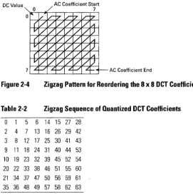
The coding model rearranges the quantized frequency coefficients into a zigzag pattern, with the lowest frequencies first and the highest fre-quencies last. The zigzag pattern (shown graphically in Figure 2-4 and numerically in Table 2-2) is used to increase the run-length of zero co-efficients found in the block. The assumption is that the lower frequen-cies tend to have larger coefficients and the higher frequenfrequen-cies are, by the nature of most pictures, predominantly zero. As illustrated in Figure 2-4, the first coefficient (0,0) is called the DC coefficient and the re-maining coefficients are AC coefficients. The AC coefficients are tra-versed by the zigzag pattern from the (0,1) location to the (7,7) location.
2.4
8x8 OCT Coefficient Block
Y Component Matrix
16 11 10 16 24 40 51 61
12 12 14 19 26 58 60 55
14 13 16 24 40 57 69 56
14 17 22 29 51 87 80 62
18 22 37 58 68 109 103 77
24 35 55 64 81 104 113 92
49 64 78 87 103 121 120 101
72 92 95 98 112 100 103 99
Cb Cr Component Matrix
17 18 24 47 99 99 99 99
18 21 26 66 99 99 99 99
24 26 56 99 99 99 99 99
47 66 99 99 99 99 99 99
99 99 99 99 99 99 99 99
99 99 99 99 99 99 99 99
99 99 99 99 99 99 99 99
[image:31.508.134.452.70.472.2]99 99 99 99 99 99 99 99
Figure 2-3 Psychovisual Weighting Functions for the Luminance and
Chrominance Components
DC Value
[image:32.508.49.321.77.349.2]7
Figure 2-4
Table 2-2
0 5
2 4 7 3 8 12 9 11 18 10 19 23 20 22 33 21 34 37 35 36 48
6 13 17 24 32 38 47 49
AC Coefficient Start 7
AC Coefficient End
Zigzag Pattern for Reordering the 8 x 8 OCT Coefficients
Zigzag Sequence of Quantized OCT Coefficients
14 15 27 28 16 26 29 42 25 30 41 43 31 40 44 53 39 45 52 54 46 51 55 60 50 56 59 61 57 58 62 63
The DC coefficients of subsequent blocks often vary only slightly. Therefore, differences between successive DC coefficients are small. The coding of the DC coefficient exploits this property through Differ-ential Pulse Code Modulation (DPCM). This technique codes the differ-ence (Delta) between the quantized DC coefficient of the current block and the DC coefficient of the previous block. The formula for the encod-ing of the DC code is:
Deltak= DC(O,O)k - DC(O,O)k_1
The inverse calculation takes place at the decoder.
The quantized AC coefficients usually contain runs of consecutive ze-ros. Therefore, a coding advantage can be obtained by using a run-length technique, where the upper four bits of the code symbol indicate
2.5
2.6
Entropy Encoding
2.7
Summary of JPEG
Baseline
the number of consecutive zeros before the next coefficient and the low-er four bits indicate the numblow-er of significant bits in the next coefficient. Following the code symbol are the significant bits of the coefficient, the length of which can be determined by the lower four bits of the code. The inverse run-length coder translates the input coded stream into an output array of AC coefficients. It takes the current code and appends to the output array the number of zeros corresponding to the four bits used for the run-length code. The coefficient placed in the output array has the number of bits determined by the lower four bits of the run-length code and a value determined by the number of trailing bits.
The block codes from the DPCM and run-length models can be further compressed using entropy encoding. For the baseline JPEG method, the Huffman coder is used to reduce entropy. One reason for using the Huff-man coder is that it is easy to implement by means of a look-up table in hardware. To compress data symbols, the Huffman coder creates shorter codes for frequently occurring symbols and longer codes for occasion-ally occurring symbols. Many applications may use predefined Huff-man tables. Therefore, the baseline encoder can operate as a one-pass or two-pass system. In the one-pass system, predetermined Huffman ta-bles are used, whereas in the two-pass system, Huffman tata-bles are cre-ated that are specific to the image to be encoded.
The first step in creating the Huffman codes is to create a table assigning a frequency count to each symbol. Symbols with a higher probability are assigned shorter codes than the less frequently occurring symbols.
The baseline system provides efficient lossy image compression. It sup-ports four color components simultaneously, with a maximum number of eight input bits for each color pixel component.
The basic data entity is a block of 8 x 8 pixels. However, this block can represent a large sub-sampled image area (for example, sub-sampled by decimated chrominance signals). The blocks of the different color com-ponents are sent interleaved, thereby allowing the decoder to create the decompressed image and translate back to the original color space on the fly.
Signal Descriptions
This chapter describes the signals that comprise the external physical interface to the CL550 and CL560. The information presented for each signal includes the signal name and mnemonic, type (input, output, or bidirectional), and description. For information about the functional op-eration of these parts, see Chapters 4 and 5. For timing information, see Chapter 6.
This chapter is divided into two sections that correspond to the compo-nents that interface to the CL550 and CL560:
o 3.1, Host Interface o 3.2, Video Interface
-DMA
Interrupt
..
-..
-Timing and Con trol
.-...
-
--Host Data Transfer Interface-
--DMA ... Interrupt II(Timing and Con trol
.-...
-...""'-..
~...
,..
,.....
~ ,.. ....
...
~..
,.....
, ~ ~...
-..
,.. ... ,..~ "PXRE 10[3:0] PXWE
PXTN
mID f5XOUT
OMA_MSTR STlill NlVlRTI HSVf\JC
HALFJULL VSVl\fC
BIANK
START
T1'vi[2:0] PXCLK
TM1JUT PXPHASE
FRf\ilET\JIT CLK3 HBCLK
RtSET TEST
CL560
HBUS[31:0] PXADR[15:0]
mrnur
PXDAT[23:0]~ PXR"E 10[3:0] PXWE PXTN
mID f5XOUT
OMA_MSTR STlill TRID HSVf\JC
IRQ2 VSVl\fC
BIANK
START
m[2:0] PXCLK
TM1JUT PXPHASE
FRliilEf\Jlj CLK3 HBCLK
RtSET
[image:35.508.122.438.69.571.2]TEST
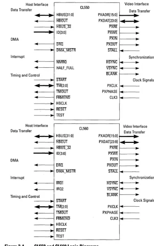
Figure 3-1 CL550 and CL560 Logic Diagrams
3-2 C-Cube Microsystems
--~..
,. ~-
... Synchr onization.
..
-
~.
Cloc k Signals
~
~
-
...-Video Inte rface sfer Data Tran .... r
-
..
... ,. .. ~ ... ,...
~ ,.. ....-Synch ronization ....- .~ ~ ... ... ,..Clo ck Signals
The CL550 external interface differs from the CL560 by only two pins:
Table 3-1 CL550 and CL560 Redefined Signal Pins
CL560 CL550 CPGA MQUAD Signal Signal Pint Pint
lRITf NKilRTI 70 013
IRQ2 HALF_FULL 135 L2
The Host Interface signals divide logically into these functional groups: o Data transfer signals: These signals comprise the address and
data bus and various control signals used to complete the data transfer handshake.
o DMA signals: These signals are used to implement a handshake
during a DMA transfer.
o Interrupt signals: These signals provide interrupt requests to the
host processor.
o Timing, control and status signals: These signals include the
clocks and reset signals.
3.1.1 Data Transfer Signals
Table 3-2
HBUS[31:0] Host Bus Bidirectionals
HBUS is the multiplexed host processor data and address bus. The width of both the address bus and the data bus can be pro-grammed to be 16-bits or 32-bits wide. The signals HBUS_32
and ID[3:0] determine the widths as shown in Table 3-2.
HBOS_32 and ID[3:0] are discussed later in this section.
Address and Data Bus Configuration
10[3:0] H8US_32 Description 0000
a
16-bit address, 32-bit data 0000 16-bit address, 16-bit data 1 h - Eha
32-bit address, 32-bit data 1 h - Eh 1 32-bit address, 16-bit data 1111 (Fh) 0/1 Chip disabled3.1
HBODT Host Bus Output Output
The Host Bus Output signal controls the direction of the host bus transfer. The CL550 and CL560 do not have sufficient drive capability to be connected directly to most computer host bus-ses. When external drivers are used, HBaDT controls the direc-tion of these buffers. When this signal is low (0), the transceiver direction is from the CL550 or CL560 to the host bus (output). When this signal is high 0), the direction is from the host bus to the CL550 or CL560 (input).
Host Bus Width = 32-bits Input
HB OS_32 is a static signal used to configure the width of the
host bus data path during CODEC accesses. When HBUS_32 is low (0), reads and writes to the CODEC register are 32-bits wide. When HBUS_32 is high (1), reads and writes to the CO-DEC register are 16-bits wide. The data path to all on-chip reg-isters except the CODEC register is always 16-bits wide.
ID[3:0] Address Space ID Signals Inputs
The address space identification signals, ID[3:0], are inputs that select the address range of the chip. Setting ID[3:0] to Ox! through OxE selects an address region for the CL550 or CL560. The ID signals allow the CL550 or CL560 to be placed in one of fourteen locations in the upper 1116 of the memory.
3.1.2 DMA Signals
The CL560 is capable of acting as either a bus slave for CODEC trans-fers, or a bus master when used with an external DMA controller. DMA transfers are fully discussed in Chapter 4, Host Interface.
DMARequest Open-Drain Output
The DRQ signal is an output that provides chip status for DMA interface control. The DRQ output is controlled by the Flag Register bits, and enabled using the DMA mask register de-scribed in Chapter 7, Registers. The DRQ output is an open-drain output and should be tied to VCC through a resistor of at least 625 ohms.
DMA_MSTR DMA Master Input
DMA_MS1R is an input that allows the CL560 to work with a
DMA controller functioning as a bus master for CODEC
fers. It is sampled on the falling edge of HBCLK when the
START signal is active. DMA transfers are fully discussed in Chapter 4, Host Interface.
Note: The CL550 does not work correctly in the DMA master mode, and in systems that use the CL550,
DMA_MSTR
should always be held HIGH. Refer to Chapter 4, Host Inter-face for a solution to this problem.
3.1.3 Interrupt Signals
NMRQ Interrupt Request Open-Drain Output
Note:
NMRQ
is a CL550 signal only. The CL560 uses TJ[(;[Iinstead.
Interrupt Request (NKiIRQ) is an unlatched output signal, syn-chronous to HBCLK, that provides an indicator of both FIFO and video field status. It can be programmed to selectively indi-cate active status flags as specified in the Interrupt Mask Regis-ter. This signal is an open-drain output and should be tied to VCC through a resistor of at least 625 Ohms (4.7K Ohms rec-ommended). On power-up, the CL550 or CL560 should be hardware reset to prevent the generation of spurious interrupts.
HALF_FULL FIFO HALF_FULL Output
Note: HALF _FULL is a CL550 signal only. The CL 560 uses IRQ2 instead.
The HALF_FULL signal is an output that indicates the status of the internal FIFO. A value of 1 (HIGH) indicates that the FIFO contains alleast 64 entries out of 128. Transitions of HALF_-FULL are synchronous to PXCLK.
IRQI
IRQ2Interrupt Request Interrupt Request
Open-Drain Output Output
Note: TJ[(;[I and IRQ2 are CL560 signals only. The CL550 uses
NMRQ
and HALF _FULL instead.syn-chronous to HBCLK. IRQl is an open-drain output while IRQ2 has a totem-pole output.
3.1.4 Timing and Control Signals
A host bus transaction consists of two (or more) bus clock cycles. Dur-ing the first cycle, the Start cycle, the host processor must indicate to the CL550 or CL560 what kind of transaction will occur (bus slave mode read, bus master mode write, etc.) by placing specific values on
TM[2:0] and DMA_MSTR. m[2:0] act as outputs during the last bus
clock cycle of the transaction, called the Acknowledge cycle. The value
output on m[2:0] indicates either that the transfer completed
success-fully or that an error occurred. In between the start and the acknowledge cycle, an indeterminate number of wait cycles can occur. Host bus transactions are fully discussed in Chapter 4, Host Interface.
START Start a Transfer Input
The START input signal begins a data transfer. When asserted LOW, it indicates that there is a valid address on the host bus (HBUS[3l:0]). START is sampled on the falling edge of HB-CLK, and should not be asserted for more than one HBCLK pe-riod.
Transfer Mode 0 Bidirectional
In bus slave mode operation, TMU is an output line that transi-tions to 0 (along with TMT) during the bus transaction acknowl-edge cycle to indicate that the transaction completed. In CL550 bus master mode only, TMU is an input, sampled during the as-sertion of TM2 (along with TMT), to determine whether a bus error has occurred. The value of TMU is ignored during a Start cycle.
TMI Transfer Mode 1 Bidirectional
The CL550 and CL560 sample the TMT input during the Start cycle to determine whether the transaction is a read or a write. A low value (0) indicates a write cycle, and a high value (l) in-dicates a read cycle. During a bus slave cycle, TMI returns to 0 during the acknowledge cycle. During a bus master mode Start cycle, the sense of this signal is inverted so that a low value in-dicates a write cycle and a high value inin-dicates a read cycle.
Transfer Mode 2 Bidirectional TN.f2 is the acknowledge signal that is driven active LOW (0) by the CL550 or CL560 during a bus slave mode acknowledge cycle. In bus master mode, this signal is driven by an external source to indicate that the transfer is complete.
TMOUT Transfer Mode Output Output
The TMOUT signal provides transceiver directional control for the transfer mode control lines TM[2:0]. If this signal is low (0), the transceiver direction is from CL550 or CL560 out to the host bus. If the signal is high 0), the transceiver direction is from the host bus into the CL550 or CL560.
FRMEND Frame End Open-Drain Output
The FRMEND signal is an output that indicates that the end of an image has been reached. This signal is an open-drain output and should be tied to VCC through a resistor of at least 625 Ohms (recommended value = 4.7K Ohms). In the CL550, dur-ing compression, FRMEND goes active when the Huffman coder has removed the last word from the FIFO. During decom-pression, FRMEND indicates that the last word has been re-moved from the Strip buffer RAM. This signal can be disabled by setting bit I of the Configuration register to a zero (See Chapter 7, Registers). In the CL560 this signal is also controlled by the Frame End Enable register (See Chapter 7, Registers). Transitions of FRMEND are synchronous to HBCLK.
HBCLK Host Bus Clock Input
HBCLK is the clock signal used to synchronize host bus data transfers. The falling edge of HBCLK is used to sample the host bus data and control signals, while the rising edge of HBCLK is used to drive the output signals. HBCLK must be the same rate or slower than PXCLK.
RESET Reset Input
TEST Test Input
The TEST signal is an input the forces all CL550 or CL560 out-puts to a high-impedance state. This feature is provided to sim-plify board-level diagnostics. TEST should be tied low for normal operation.
3.2
The Video Interface signals divide logically into these functionalVideo Interface
groups:D Pixel Bus Data Transfer Signals: These signals comprise the
vid-eo data bus, the Strip Buffer address bus, and the handshake sig-nals necessary to transfer data.
D Video Synchronization Signals: These are the signals used to
con-trol the horizontal and vertical placement of the video frame.
D Video Clock Signals: These are the timing signals necessary for
the CL550 and CL560 to operate.
3.2.1 Pixel Data, Address and Handshake Signals
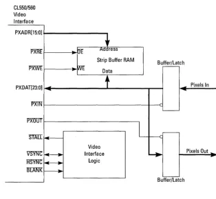
3-8 C-Cube Microsystems
PXDAT[23:0] Pixel Data Bus Bidirectionals
PXDAT is a bidirectional 24-bit bus that handles uncompressed or decompressed pixel data. In the compression mode, uncom-pressed video data is input on PXDAT[23:0] and comuncom-pressed data is output on the host bus. In the decompression mode, com-pressed data is input on the host bus and decomcom-pressed video data is output on PXDAT[23:0]. PXDAT is also used to transfer data to and from the strip buffer RAM. In some modes (Gray-scale, YUV 4:2:2 and CMYK), only 16 of the 24 bits are used. The unused pins should be tied to ground through 10K-ohm re-sistors.
PXADR[15:0] Pixel Address Outputs
PXADR is the address bus for the strip buffer RAM. The 16 bits of address support a strip buffer of up to 64K entries.
PXRE Pixel Read Output
is active only when pixels are being read from the strip buffer RAM out to the pixel destination.
PXWE Pixel Write Output
The PXWE output is designed to directly control the write en-able input to the strip buffer RAMS. During compression, PXWE is active only during PXIN cycles when pixel data is be-ing written from the active portion of the video field into the strip buffer RAM. During decompression, PXWE is active only when active pixels are being written from the CL550 or CL560 into the strip buffer RAM.
CL550 or CL560
To Host Processor
PXDAT[23:0j ~
..
....
~
,Strip Buffer RAM 64K x 32
PXADR[15:0j
t
Figure 3-2
PXWE PXRE
Strip Buffer RAM Connections
Pixel Input Control Output
The PXIN signal is used to activate an input buffer on the Pixel Data bus, PXDAT, during input cycles. It is asserted (LOW) only when pixel data is being input from the active portion of the video field into the Strip buffer RAM.
pxOUt
Pixel Output Control OutputStALL
Stall Input This input signal, when asserted (LOW), will stop all activity on the Video Interface in its current state. Signals affected bySTAII include PXADR[l6:0], PXDAT[23:0], PXRE, PXWE, PXIN, PXOO'C BLANK, VSYNC and HSYNC. Use of the
STAII signal in discussed completely in Chapter 5, Video In-terface.
3.2.2 Video Synchronization Signals
3-10 C-Cube Microsystems
HSYNC
Horizontal Sync BidirectionalHSYNC is a bidirectional signal used to indicate the start of a
horizontal line. When the CL560 is programmed for master mode operation (Configuration register bit 3 = 1), the HSYNC
signal functions as an output and is asserted (LOW) when the CL560 is about to begin a new line. The duration of the pulse is programmed using the HSYNC register.
When in slave mode (Configuration register bit 3 = 0), the
HSYNC line functions as an input, and the external pixel
inter-face must assert this signal to begin the next line. The HSYNC
input is negative-edge triggered.
VSVNC
Vertical Sync BidirectionalVSYNC is a bidirectional signal used to indicate the start of a
frame. When the CL560 is programmed for master mode oper-ation (Configuroper-ation register bit 3 = 1), the VSYNC signal func-tions as an output and is asserted (LOW) when the CL560 is about to begin a compression or decompression operation. The duration of the pulse is programmed using the VSYNC register. When in slave mode (Configuration register bit 3 = 0), the
YSYNC line functions as an input, and the external pixel
inter-face must assert this signal after writing to the HVEnable and Start registers to begin a compression or decompression opera-tion. The YSYNC input is negative-edge triggered.
BLANK
Blanking OutputThis signal is an output that indicates that there are no active pixels on the Pixel Data bus. BLANK changes state at the same time as the PXADR bus (at the beginning of the Strip buffer read cycle, when PXPHASE is HIGH). During compression,
is written to the Strip buffer, and goes LOW again after the last pixel is written. During decompression, BLANK negates simul-taneously with the first active pixel read, and asserts one PX-CLK after the last pixel read.
3.2.3 Video Clock Signals
PXCLK Pixel Clock Input
The PXCLK signal is the main clock for the compression pro-cessor. All circuits except those directly related to the host bus interface are driven by this clock.
PXPHASE Pixel Phase Input
The value of the PXPHASE input signal indicates whether a Strip buffer read or write operation is occurring on the pixel bus. This signal should be one-half the frequency of PXCLK. If PX-PHASE is high during the rising edge of PXCLK, the cycle is a Strip buffer write operation.
CLK3 Clock Three Input
Host Interface
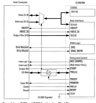
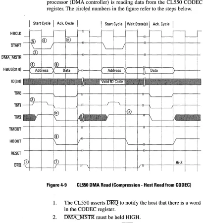
The Host interface on the CL550 and CL560 is designed to be connect-ed to a variety of general-purpose microprocessors with a minimum of external logic. The host processor can directly access any CL550/560 register or memory address by reading or writing specific memory ad-dresses. The host can also access CL560 data using DMA transfers. DMA transfers are provided as a fast method of transferring data to and from the CODEC FIFO. The host bus interface also includes signals for timing and control, status and interrupt processing.
This chapter is divided into sections which describe how the host inter-face is used. These sections are:
D 4.1, Register Access Timing D 4.2, DMA Access Timing D 4.3, Control Signals
Host Computer CL550/560
CODEC
11_
,...
.1
D[31:011
Data [31:0] ~
---
,.-
Host Interface Address [31 :0] "" ,.v. ""
-
D[15:0]HBUOT
-
HBUOTHBUS::]2 HBUS::]2
Output Bits [3:0] "'"
-
10[3:0]DMA Logic
Dma Request <I URTI
-Dma Master
o
Mj'CMSTR Timing and ControlInterrupt 1 TRTIf[NMRIT] Interrupt 2 <I IRQ2 [HALF FULL]
-Output Bit START
I/O Bits ~ ...
~
I ~ i ... TM[2:0]-
,.I
-
,.+
TMTIUT Input Bit ~ fRMEI'\JIT-Clock ~ HBCLK
Reset
..
RtS"ET..
TEST [CL550 Signals]J-
-Figure 4-1 CL550 and CL560 Host Interface Block Diagram
The CL560 host bus interface differs from the CL550 interface in sev-eral ways:
4-2 C-Cube Microsystems
[image:47.505.129.452.126.470.2]IRQ2 Interrupt Mask registers (See Chapter 7, Registers). o The CL550 signals DRQ (data request) and FRMBND (frame end)
operate differently in the CL560, although they retain the same name. These differences are described in Chapter 3, Signal De-scription.
o The CL560 samples the input data at a different point than the CL550. This difference is described in Chapter 6, Specifications. o The signals TMU, TIVIT and TML have timing differences between
the CL550 and the CL560. These differences are described in Chapter 6, Specifications.
o The signals HBOOT and TMOOT have timing differences be-tween the CL550 and the CL560. These differences are described in Chapter 6, Specifications.
If you are designing a system that will accept both the CL550 and the CL560, the only signals that have had their external function redefined are: Table 4-1 CL560 Signal
mrrr
IRQ2CL550 and CL560 Redefined Signal Pins
CL550 Signal Nl\ifRTI HALFJULL CPGA Pint 70 135 MQUAD Pint 013 L2
This section describes the timing for register accesses. It is divided into
4.1
these subsections:o 4.1.1, Signal Descr.1Ptions o 4.1.2, Register Access Timing o 4.1.3, Host Bus Register Access o 4.1.4, Host Bus Register Write
4.1.1 Signal Descriptions
All CL550/560 family registers and memory are accessed using register accesses except the CODEC register. The CODEC register can be ac-cessed using either register accesses (described in this section) or DMA transfers (see Section 4.2). The following signals are used to access the CL550/560 part in register access mode:
D HBCLK, Host Bus Clock: All host bus accesses are synchro-nized to the Host Bus Clock. The falling edge of HBCLK is used to sample the host bus data and control signals, while the rising edge of HBCLK is used to drive the output signals.
D HBUS[31:0], Host Bus: HBUS[31 :0] is a multiplexed data and
address bus. The signal START is used to indicate that an address is present on the bus. The width of the host bus can be either 16 or 32-bits wide depending on the signals ID[3:0] and HBOS_32. D
START,
Transaction Start: The START signal begins a datatransfer. When asserted, it indicates that there is a valid address on HBUS[31 :0]. START is sampled on the falling edge of HBCLK, and should not be asserted for more than one HBCLK period.
D ID[3:0], Address Space Identification Signals: ID[3:0] are
in-puts that select the address range of the chip. When the part re-ceives a START signal, it compares the value on ID[3:0] with the address on HBUS[31 :0] bits 27 through 24. If a match occurs, an internal chip select signal is generated.
Figure 4-2 10[3:0] Chip Select Address Format
To generate a valid chip select, the contents of HBUS [31: 16] should be as shown in Figure 4-2, where X = Don't Care. This allows the CL550/ 560 part to be placed in anyone of fourteen locations in the upper 1116th of memory.
Setting ID to OxO overrides the decoding of the upper 16-bits of the ad-dress, putting the CL550/560 part into a 16-bit address mode. Setting ID to OxF disables the host bus interface.
D
HBUS_32,
32-bit Host Bus:HBOS_32 is a static signal used to
configure the host bus data path width during CODEC accesses. When HBOS_32 is low, the read/write path to the CODEC regis-ter is 32-bits wide. When HBUS_32 is high, the read/write path tothe CODEC register is 16-bits wide. The data path to all on-chip registers and tables except for the CODEC register is always 16-bits wide. In the 16-bit data mode, HBUS[31:16] remain disabled (three-stated) at all times and transfers take place over
HBUS[l5:0].
HBOS_32 and ID[3:0] combine to control the address and data modes
as shown in Table 4-2.Table 4-2 Address and Data Bus Configuration
10[3:0] HBUS_32 Description 0000 0 16-bit address, 32-bit data 0000 1 16-bit address, 16-bit data 0001-1110 0 32-bit address, 32-bit data 0001-1110 32-bit address, 16-bit data
1111
o
or 1 Chip DisabledD
TMU,
Transfer Mode 0: In register access mode operation,TMU
is an output line that transitions to 0 (along with TMI) during the bus transaction acknowledge cycle to indicate that the transaction completed. The value ofTMU
is ignored during a Start cycle. DTID,
Transfer Mode 1: The CL550/560 part samples the TMTinput during the Start cycle to determine whether the transaction is a read or a write. TM 1 changes sense between register access cycles and DMA access cycles. During register access cycles, a low value (0) on TMI indicates a write cycle, and a high value (1) indicates a read cycle. During DMA cycles, a high value (1) on TM 1 indicates a write cycle, and a low value (0) indicates a read cycle. During a register access cycle, TMT returns to 0 during the acknowledge cycle.
D
TID,
Transfer Mode 2: TM2 is the acknowledge signal that is driven active (0) by the CL550/560 family during a register accessacknowledge cycle.
D
TMOUT,
Transfer Mode Control Lines=
Outputs: TheTMOOT signal provides transceiver directional control for the
transfer mode control lines TM[2:0]. If this signal is low (0), the transceiver direction is from the CL550/560 part out to the hosthost bus into the part.
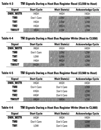
[image:51.510.137.459.172.588.2]The tables below show the values of the CL550/560 control signals dur-ing each of the three bus access cycles. Table 4-3 and Table 4-4 show the CL550 control signals, and Table 4-5 through Table 4-8 show the CL560 control signals. The shaded areas indicate that the signals are driven as outputs.
Table 4-3 TM Signals During a Host Bus Register Read (CL550 to Host)
Signal OMA_MSTR TMO TM1 1M2 TMOUT Start Cycle HIGH Don't Care HIGH
Wait State(s) Acknowledge Cycle
HIGH HIGH
Table 4-4 1M Signals During a Host Bus Register Write (Host to CL550)
Signal oMA_MSTR TMO TM1 1M2 TMOUT Start Cycle HIGH Don't Care LOW
Wait State(s) Acknowledge Cycle
HIGH HIGH
Table 4-5 TM Signals During a Host Bus Register Read (CL560 to Host)
Signal oMA_MSTR TMO TM1 1M2 TMOUT Start Cycle HIGH
Wait State(s) Acknowledge Cycle
HIGH HIGH
Table 4-6
TM
Signals During a Host Bus Register Write (Host to CL560)Signal oMA_MSTR TMO TM1 Start Cycle HIGH Don't Care LOW Wait State(s) HIGH Don't Care Don't Care Acknowledge Cycle HIGH
Table 4-6
TM
Signals During a Host Bus Register Write (Host to CL560)Start Cycle Wait State(s) Acknowledge Cycle
---=~---Table 4-7 WSignals During a DMA Read (CL560 to Host)
Signal Start Cycle Wait State(s) Acknowledge Cycle
DMA_MSTR LOW HIGH HIGH
TMD Don't Care Don't Care Don't Care
TMf LOW Don't Care Don't Care
TM2 HIGH HIGH LOW
TMOUT
Table 4-8 TM Signals During a DMA Write (Host to CL560)
Signal Start Cycle Wait State(s) Acknowledge Cycle
DMA_MSTR LOW HIGH HIGH
TMD Don't Care Don't Care Don't Care
TMf HIGH Don't Care Don't Care
TM2 HIGH HIGH LOW
TMOUT
D
BBOUT,
Host Bus=
Output: TheHBOOT
signal is used to con-trol the direction of the host bus transfer. The CL550/560 does not have sufficient drive capability to be connected directly to most computer host buses. When external drivers are used,HBOOT
is used to control the direction of these buffers. When this signal is low (0), the transceiver direction is from the CL550/560 to the host bus (output). When this signal is high 0), the direction is from the host bus to the part (input).4.1.2 Register Access Timing