warwick.ac.uk/lib-publications
Original citation:
Hu, Borong, Ortiz Gonzalez, Jose Angel, Ran, Li, Ren, Hai, Zeng, Zheng, Lai, Wei, Gao, Bing, Alatise, Olayiwola M., Lu, Hua, Bailey, Christopher and Mawby, P. A. (Philip A.). (2017) Failure and reliability analysis of a SiC power module based on stress comparison to a Si device. IEEE Transactions on Device and Materials Reliability, 17 (4). pp. 727-737.
Permanent WRAP URL:
http://wrap.warwick.ac.uk/97325
Copyright and reuse:
The Warwick Research Archive Portal (WRAP) makes this work by researchers of the University of Warwick available open access under the following conditions. Copyright © and all moral rights to the version of the paper presented here belong to the individual author(s) and/or other copyright owners. To the extent reasonable and practicable the material made available in WRAP has been checked for eligibility before being made available.
Copies of full items can be used for personal research or study, educational, or not-for profit purposes without prior permission or charge. Provided that the authors, title and full bibliographic details are credited, a hyperlink and/or URL is given for the original metadata page and the content is not changed in any way.
Publisher’s statement:
“© 2017 IEEE. Personal use of this material is permitted. Permission from IEEE must be obtained for all other uses, in any current or future media, including reprinting
/republishing this material for advertising or promotional purposes, creating new collective works, for resale or redistribution to servers or lists, or reuse of any copyrighted component of this work in other works.”
A note on versions:
The version presented here may differ from the published version or, version of record, if you wish to cite this item you are advised to consult the publisher’s version. Please see the ‘permanent WRAP URL’ above for details on accessing the published version and note that access may require a subscription.
Abstract—The superior electro-thermal properties of SiC power devices permit higher temperature of operation and enable higher power density compared with silicon devices. Nevertheless, the reliability of SiC power modules has been identified as a major area of uncertainty in applications which require high reliability. Traditional power module packaging methods developed for silicon chips have been adopted for SiC and the different thermomechanical properties cause different fatigue stresses on the solder layer of the chip. In this paper a 2-D Finite Element (FE) model has been developed to evaluate the stress performance and lifetime of the solder layer for Si devices, which has been validated using accelerated power cycling tests on Si IGBTs. The proposed model was extrapolated for SiC devices of the same voltage and current rating using the same solder material and the results show that under the same cyclic power loss profile the induced stress and strain energy in the die attach layer is much higher and concentrates on the die/solder interfacial area for SiC chips. Using the validated stress-based model, the lifetime can be quantified when SiC chips are used. This ability to extrapolate the available power cycling and lifetime data of silicon chips to silicon carbide chips would be a key element for developing reliable packaging methods for SiC devices.
Index Terms— Stress comparison, silicon carbide, failure analysis, power cycling, life prediction
I. INTRODUCTION
HE superior properties of silicon carbide (SiC) power devices, including higher blocking voltage, lower switching and conduction losses, and high-temperature operation ability, with respect to silicon devices [1] are fundamental assets of the wide bandgap technology. SiC power devices are now widely and commercially available, after addressing different issues related to the manufacturing process: gate dielectric instability, large leakage current due to wafer defects[2,3]and poor long-term chip tolerance at high temperatures [4,5]. Considerable progress has been made to
This work was supported by The National Key R&D Program of China (2017YFB0102303), National Natural Science Foundation of China (51607016), graduate scientific research and innovation foundation of Chongqing (CYB17008) and the UK EPSRC under Grant EP/K036327/1 and through the Underpinning Power Electronics Components Theme under Grant EP/K034804/1.
B. Hu, L. Ran, H. Ren, Z. Zeng, W. Lai and B. Gao are with the State Key Laboratory of Power Transmission Equipment & System Security and New
overcome these issues: Gate oxide reliability can now be improved by e.g. annealing in nitric oxide (NO) after oxidation to reduce oxide layer traps and ensure high effective barrier height at high temperatures. Step-controlled epitaxial growth and new trench structure can reduce the effect of material defects, thus the performance of the devices can be also improved [6, 7].
Despite of the aforementioned improvements on the fabrication of the devices, there are still concerns about the performance of the packaging system used for SiC devices. Due to direct contact of materials with different coefficients of thermal expansion (CTE), the elements of the packaging are subjected to thermomechanical stresses, caused by the variation of temperature during normal operation of the devices. The thermomechanical stresses will cause degradation of the weaker elements of the packaging system, leading to device failure [8]. Given that traditional packaging methods were developed and tested for silicon chips, the reliability of the packaging systems for SiC devices has appeared as a major concern because of the different thermomechanical properties of SiC compared to silicon. Although the CTE of SiC is closer to that of copper or aluminum, the higher thermal conductivity and Young’s modulus of SiC may cause higher stresses on the die-attach solder layer during power cycling [9]. In some applications, SiC devices may be used at higher temperatures while suffering higher temperature cycling [10, 11]. Despite the aforementioned superior electrical properties, the limited reliability of SiC power devices hinders their application in the areas like more electric aircrafts and DC grids, where a very high reliability is required.
Standard power cycling tests are used to evaluate the performance of a packaging system [2]. Power cycling can be classified as fast and slow cycling, depending on the duration of the temperature cycles. Fast power cycling is mainly conducted to estimate the reliability of the die-attach solder layer [12], while the slow cycling is carried out to produce
Technology, School of Electrical Engineering, Chongqing University, Chongqing 400044, China.
J. O. Gonzalez, O. Alatise and P. Mawby are with the School of Engineering, University of Warwick, Coventry CV4 7AL, U.K. L. Ran is also with the School of Engineering, University of Warwick, Coventry CV4 7AL, U.K.
H. Lu and C. Bailey are with School of Computing and Mathematical Sciences, University of Greenwich, London SE10 9LS, U.K.
Failure and Reliability Analysis of a SiC Power
Module Based on Stress Comparison to a Si
Device
Borong Hu, Jose Ortiz Gonzalez, Li Ran, Hai Ren, Zheng Zeng, Wei Lai, Bing Gao, Olayiwola Alatise, Hua Lu, Christopher Bailey, Phil Mawby
fatigue on the baseplate solder layer. In this study, the main concern of reliability is the die-attach solder layer so fast power cycling has been selected. Using this power cycling strategy, the die-attach solder layer undergoes frequent temperature cycling with sizable value of temperature fluctuation [13]. Aged die-attach solder layer impedes the heat extraction from the chip, hence increasing the thermal impedance and junction temperature. Generally, the die-attach solder layer will degrade earlier than other failure mechanism appearing during power cycling - bond wire lift-off [14], but it is not the subject of study in this paper.
Solder fatigue is caused by the plastic strain and creep during cycling [15-17]. While the SiC chip is suitable to operate at high temperatures, it can cause significant thermal stress on the solder layer leading to substantial fatigue [17-19]. Experimental results from different samples reveal that the shear stress in a SiC die-attach is higher than that in a Si device [20], and strain energy density tends to concentrate at the chip edge where the difference is 1.5 times between the SiC and Si devices under comparable conditions [9]. It is considered that the in-service lifetime of SiC solder layer is only a third of the benchmark Si device. In [21], cracks and voids are observed on the solder edges of the Si IGBTs and SiC diodes after power cycling.
Due to the low reliability of SiC die-attach in package, double-side cooling and direct liquid cooling are suggested to enhance the capability of heat dissipating and reduce the thermal stress [22, 23]. New solder materials, such as SnAg3Cu0.5, AuGe12, ZnAl5Ge0.1 and nano-silver sintering, could also provide higher reliability than the usual SnPb5 [17,20,24-26]. However, it is necessary to further investigate and understand the effect of the material properties of SiC itself on the thermomechanical stresses. Previous research only considered the static stress under certain load conditions, but the lifetime characteristic of the SiC device under dynamic and realistic operating conditions is yet to be investigated.
This paper analyzes the fatigue stress caused by the CTE mismatch between the chip and solder layer during power cycling, which causes creep strain accumulation in the solder layer when the device is operated at elevated temperature for a sustained period of time. Power cycling test is a time consuming task, even with accelerated test conditions; and the time required to obtain meaningful data is a major drawback. In the case of SiC chips, given the higher price of the devices compared with their silicon counterparts, it is a more expensive exercise. However, as the lifetime of the solder is dependent of the creep strain, using the resultant creep strain obtained when a SiC chip is used, an estimation of the lifetime can be obtained. This study attempts to extrapolate the lifetime test results from Si devices to SiC with the same solder material. This requires a physics-of failure lifetime model which can be validated using experimental power cycling results on silicon devices.
The paper is organized as follows. In section II, the 2-D Finite Element (FE) model used to analyze the fatigue of the die-attach for a silicon chip is defined and validated using experimental power cycling results of Si IGBTs. The thermal-mechanical properties and dimensions of a SiC chip are compared with the Si devices in section III. Using a lifetime
model for the solder, based on creep energy, the extrapolation of the lifetime of the die-attach solder under power cycling tests when SiC chips are used is then presented in section IV, where the fatigue performance of the die-attach is compared in terms of thermal stress, creep strain and creep energy density for Si and SiC chips. Section V concludes the paper.
II. FINITE ELEMENT MODELING AND ACCELERATED LIFETIME
TEST FOR SI DEVICES
Power cycling test is an effective and feasible tool widely used to evaluate the lifetime of power modules and devices. In case of Si power modules, there are large amounts of available lifetime data extracted from power cycling tests based on matured techniques both in cycling strategy and junction temperature monitoring. In the case of SiC power modules, considering the large quantity of samples required to obtain enough data to ensure the accurate prediction of lifetime, it would be more expensive due to the difference in price between silicon and silicon carbide power modules.
The different thermomechanical properties of Si and SiC chips have been suggested as the cause of the different power cycling capabilities of their modules. The failure process of solder layer is only related to the stress performance of solder material and considering that the standard commercially available Si and SiC power modules have the similar packaging materials, it would be possible to establish a stress comparison between Si and SiC devices to estimate the lifetime of SiC die-attach solder layer.
Given the time consumed by the power cycling tests, it would be beneficial that the power cycling capability of SiC devices could be obtained as soon as possible, especially from the point of view of the packaging design. Well-known physical lifetime models for the solder die-attach are based on fatigue stress and strain. Due to the difficulty of measuring the stress or strain in the solder layers directly, Finite Element (FE) model is adopted to evaluate the stress [27].
A. Finite Element Modeling
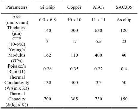
The test vehicle proposed for the evaluation of the stresses on the solder consists of an Al2O3 Direct Bonded Copper (DBC) [28] substrate of dimensions 11 mm by 11 mm with thicknesses of 300 μm/ 630 μm/ 300 μm for the Cu/ Al2O3/Cu layers, where the die is attached to the substrate using a layer of SnAg3Cu0.5 (SAC305) solder with a thickness of 120 μm. The selected chip is a 1200 V/50 A silicon IGBT, with datasheet reference SIGC41T120R3E. A 3D view and a cross-section of the test vehicle are shown in Fig. 1.
The dimensions and materials of chip, die-attach solder layer and DBC layer selected for FE model are the same as the IGBT module selected for the later experimental accelerated tests. The dimensions of the chips are presented in Table I, where the principal thermomechanical properties are also identified, together with the dimensions and thermomechanical properties of the die-attach solder and DBC substrate.
evaluation of the stresses on the solder layer involving strain and temperature effect, assuming that plastic flow occurs at all nonzero stress value. This model accounts for the physical phenomenon of strain-rate, strain hardening or softening characteristics, crystalline texture and its evolution, and it does not require an explicit yield condition [29].
The material properties of the solder layer for the Anand’s model are shown in Table II, where s0is the initial deformation
resistance, Q/R the ratio of activation energy to Boltzmann’s constant, A pre-exponential factor, the stress multiplier, m0 and
ŋ the strain rate sensitivity of stress and strain rate sensitivity of the saturation value, h0 the hardening/softening constant, s the coefficient for the saturation value of deformation resistance and a the strain rate sensitivity of the hardening/softening.
The centers of each layer of the material are coincident and
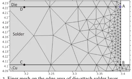
the 3D model presented can be simplified to a 2-D model, as it is shown in Fig. 1. The 2D sections were obtained by cutting from the symmetric centerline plane along the direction of the longer side of the chip. The calculation method of 2D modeling in COMSOL is an approximation that the 2D model has a thickness in depth as a “cube”. The 2D section then should be selected in symmetric centerline, which will be more realistic in the dimensions of the test vehicles when it is assumed as a “cube” in FE calculation, rather than in diagonal. The thermomechanical performance is also symmetrical in the 2D symmetry section of the cutting plane obtained for modeling. This simplification has been verified more than 90% accuracy as compared with a 3D model when used for calculation of strain energy in FE model, and can be representative of a 3D fatigue analysis of the solder layer [30]. The 2D symmetric FE model in COMSOL Multiphysics software built for this study is presented in Fig. 2.
The higher stresses are concentrated on the edges of the die/solder interface [31], hence a finer mesh is utilized for this area, in order to evaluate in more detail and with higher precision the thermal stress and strain. The fixed number of mesh elements distributed on the die/ solder interface is 60 elements for Si model, and the mesh number distributed on the solder edge is fixed as 10 elements. The boundary conditions of FE modeling are set as follows: the whole chip is the power source of heat defined by general source distributed in the chip volume homogenously; the bottom of DBC is the roller fixed (the normal displacement is fixed); convective heat flux is defined to emulate the heat dissipation of forced water-cooling (plate length is 0.5 m and fluid velocity is 3 m/s) on the bottom copper surface of DBC ; the left-hand side edge of the model (as shown in Fig. 2) is the symmetrical boundary; the rest of the open surfaces are set as free-to-move without constraints and they are also set as thermal insulation to reduce the interference factors.
[image:4.612.68.257.127.302.2]A detail of the area of interest is shown in Fig. 3. The stress, strain and lifetime distribution on solder layer will be evaluated later for this area, confined by four points: Point A is at the corner of the top surface on the solder layer, point B is at the corner of bottom surface, and points C and D are on the bottom and top interface respectively. The distance from point C (D) to point B (A) is 0.2mm, and the distance from A (D) to B (C) is
Fig. 1. The test vehicle for Si
TABLEI
SI DEVICE AND PACKAGING MATERIAL PARAMETERS
Parameters Si Chip Copper Al2O3 SAC305
Area
(mm x mm) 6.5 x 6.8 10 x 10 11 x 11 As chip Thickness
(μm) 140 300 630 120 CTE
(10-6/K) 3 17 6.5 23 Young’s
Modulus (GPa)
162 110 400 40
Poisson’s
Ratio (1) 0.28 0.35 0.22 0.4 Thermal
Conductivity (W/(m x K))
130 400 35 50
Thermal Capacity (J/(kg x K))
700 385 730 150
TABLE II
ANAND’S PARAMETERS DEFINITION
Parameters s0(MPa) Q/R(K) A(s-1) m 0 Solder 12.41 9400 4.1x10⁶ 1.5 0.303
Parameters h0(MPa) s(MPa) a
Solder 1378.95 13.79 0.07 1.3
[image:4.612.316.562.254.412.2] [image:4.612.55.288.330.513.2] [image:4.612.70.274.640.703.2]the thickness of the solder layer.
In this FE model coupled physics between heat transfer and solid mechanics are used. When the heat source is considered for the thermal analysis, the differential equation for the temperature calculation of the element in each layer is given by [32]
vT
k T Q c
t
(1) where k is the thermal conductivity, T the temperature, Qv the
heat source per unit volume, the density and c the specific heat.
Considering the particular properties of semiconductor chip, the mechanical behavior of chip/die-attach system on the 2-D section will be analyzed in detail here. With the simulated temperature T, the CTE mismatch between the materials on the interface would lead to unequal thermal expansion strain among these materials. As the material layers are bonded in rigid connection, they will remain at the same length when the temperature changes causing a tendency of deformation. Assuming that the length of chip and solder both are L0 initially
and LT is the length at a defined temperature T, equation (2) can
be used for calculating the constrained strain of each layer [33].
00 T ref L L T T L
(2)
where is the constrained strain of the layer of interest, the CTE of the material and Tref the reference temperature. The
residual stress/strain from the manufacturing process is assumed to be zero at ambient temperature 20 ⁰C, so that Tref is
set at 293.15 K in the thermo-mechanical analysis module in COMSOL software. The first term of equation (2) is the unconstrained strain while the second term refers to the actual strain at the changed temperature T. The constrained strain will induce thermal stress in each material. For example, when the chip temperature increases, the chip with a lower CTE than the solder constrains the thermal expansion of the solder interface, thus the solder will be under compression and chip will be under tension.
The stress of the concerned layer due to the constraint of CTE mismatch is given by equation (3), where E is the Young’s modulus [34] of the material.
E
(3) According to Newton’s third law, the stress of the chip and solder would be equal, hence using equation (2) the stress in thesolder can be obtained as
1 solder solder solder chip E T E E
(4)
where solder is the solder stress, Esolder and Echip are Young’s
Modulus of the solder and chip respectively, stands for the value of CTE mismatch between solder and chip, and T is the temperature swing from the reference Tref.
The impact of the material properties on the stress on the solder is determined by the Young’s modulus of the material and the CTE mismatch, as shown in equation (4), hence the impact of the semiconductor material on the stress on the solder. In the case of SiC, the Young’s modulus and thermal conductivity are all approximately 3 times higher and their influences on the temperature, stress and lifetime will be evaluated in section III and IV.
The creep energy accumulated in one cycle will be used as the fatigue indicator to estimate the solder layer lifetime. Morrow model [35, 36] proposed an exponential relation between the fatigue life and the cyclic plastic strain energy and has later been modified to estimate the lifetime of solder layer depending on creep strain energy. Given the accumulated energy for one cycle, the number of cycles to failure can be obtained from:
2
mc f f
W W N
(5)
where Nf is the number of cycles to failure, Wc the creep
energy accumulated in one cycle which can be obtained from simulation, Wf the fatigue energy coefficient of the solder
material and m the fatigue energy index. For solder SnAg3Cu0.5 used in this study, the values of Wf and m are given
in Table III.
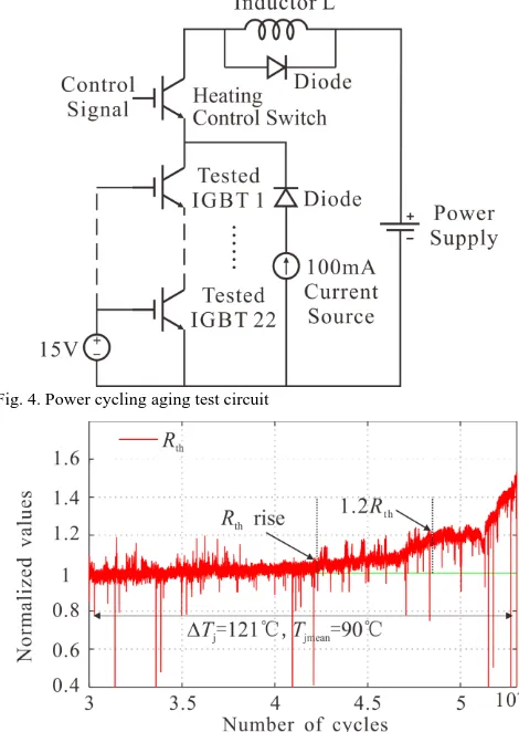
B. Power cycling tests for Si devices
In [12] power cycling tests were performed on silicon IGBT power modules and the lifetime of the solder for different junction temperature excursions and mean temperatures was obtained. The experimental setup is shown in Fig. 4 in which it is possible to test 22 IGBT devices simultaneously. The IGBT devices are permanently turned on and the heating current is controlled by an auxiliary switch to heat up the devices. When the heating current is switched off, the devices enter the cooling phase, where the thermal resistance, used as an indicator of degradation of the solder layer, is measured in each cycle by sensing the junction temperature, case temperature and power losses. The junction temperature is measured using the forward voltage at low currents (Isense=100 mA) as a Temperature
Sensitive Electrical Parameter (TSEP) [37] after the main control switch is switched off.
In the experimental accelerated tests the single-chip IGBT modules of model SKM50GB123D (rating voltage/current: 1200V/50A) with the solder material SnAg3Cu0.5 were tested
Fig. 3. Finer mesh on the edge area of die-attach solder layer
TABLE III
MORROW MODEL PARAMETERS FOR SNAG3CU0.5 SOLDER
Parameters Wf (J/m3) m
[image:5.612.57.288.190.329.2]under two groups of power cycling conditions: 1) 9 devices were set at an average junction temperature Tj,mean=90C and
junction temperature variation ∆Tj=90C, and 2) 17 devices
were set at a Tj,mean=90C and a junction temperature variation
∆Tj=120C. The thermal resistance of an IGBT module is
monitored during power cycling test as shown in Fig. 5, with an increase of 20 % of the nominal value considered an indicator of failure.
The lifetime results and temperature profiles for the 17 IGBT modules subjected to power cycling are summarized in Table IV. It should be mentioned that the differences of electrical and thermal characteristics caused by fabrication and manufacturing process among these devices under test (DUTs) are inevitable. When the DUTs connected in series in the test platform, the single current will cause varying power losses on each device during power cycling test. As all the DUTs are all mounted on one water-cooling heatsink, the device mounted near the input of cooling water has a better heat dissipation performance as compared with the one at rear position of the heatsink. These will cause minor errors of Tj,mean swing a few degree Celsius from 90 ˚C as shown in Table IV, while this small swing only has limited influence on failure process according to Coffin-Manson model.
The lifetime criterion of accelerated aging experiment is 20% thermal resistance increase corresponding to 23% crack length
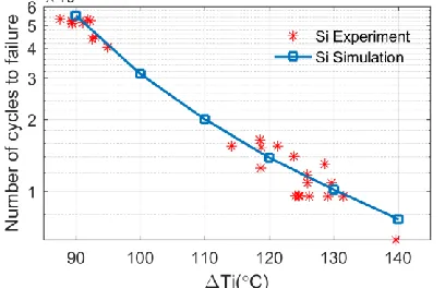
in solder layer in the FE model [38]. Although the divergence of thermomechanical performance among these DUTs is also inevitable considering the semiconductor fabrication and packaging process, the statistical results extracted from the tests could still demonstrate an evident trend of lifetimes Si module around Tj,mean=90˚C as shown in Fig. 6.
The model presented in the previous section will be validated using these experimental results, hence the same temperature profile as in the accelerated tests has been selected. The value of the mean junction temperature has been defined as Tj,mean=90C, with temperature excursions Tj of 90, 100, 110,
120, 130 and 140C. For these simulations, the junction temperature is defined as the temperature at the left-side corner of the top surface of the chip in the 2-D symmetry model as shown in Fig. 2.
The experimental results closely distributed around the results from FE simulation with a goodness-of-fit higher than 97% as shown in Fig. 7, which infers that the these results are able to validate the FE model under Tj,mean=90˚C.
[image:6.612.314.564.143.530.2]According to the results presented in Fig. 7, the FE model gives a good estimation and can show a clear trend of the
Fig. 4. Power cycling aging test circuit
Fig. 5. The normalized thermal resistance of an IGBT module during power
cycling test
TABLE IV
POWER CYCLING RESULTS OF ALL POWER MODULES UNDER TEST
No. ΔTj (C)
Tj,mean
(˚C)
Cycles to failure
No. ∆Tj (C)
Tj,mean
(˚C)
Cycles to failure
1 87.56 82.41 53030 14 121.28 89.55 15535
2 89.36 85.22 52085 15 123.84 84.01 14015
3 89.43 80.61 50780 16 124.10 83.88 9566
4 91.09 90.88 51356 17 124.55 87.08 9568
5 91.85 90.19 52932 18 124.74 83.81 9552
6 92.21 82.30 52223 19 125.85 90.24 11730
7 92.56 86.32 43775 20 125.91 86.37 10864
8 93.00 87.30 44673 21 126.19 85.47 9504
9 94.97 94.24 40472 22 128.63 90.18 13023
10 114.14 80.96 15514 23 129.12 88.90 9509
11 118.55 84.16 16462 24 129.66 87.27 10862
12 118.66 80.99 12538 25 131.49 88.91 9509
[image:6.612.314.564.145.529.2]13 118.76 85.20 15331 26 139.65 96.10 6248
[image:6.612.49.284.153.484.2]lifetime of the solder under power cycling condition when a Si chip is used. The result of Morrow’s model is only based on the thermomechanical behavior of the solder material, hence if the creep energy on the solder is calculated when a SiC chip is used the lifetime of the same solder material can be estimated. As the different properties of SiC seem to contribute the higher fatigue in its die-attach solder layer, it is necessary to understand the impact of the chip material on the temperature distribution and stresses on the solder during power cycling before extrapolating the lifetime of SiC.
III. FINITE ELEMENT MODELING OF SICDEVICE AND
TEMPERATURE PROFILE OF POWER CYCLING
The FE modeling method for lifetime evaluation of the solder layer was validated using accelerated lifetime tests using Si IGBTs. The model is based on the creep energy on the solder, hence if the same solder material is used for both Si and SiC chip, the lifetime of the solder as a function of the chip material can be investigated. However, it is first necessary to understand and evaluate how the change of the chip material affects the stresses on the solder.
The test vehicle used for the study of the impact of the semiconductor material on the stresses in the solder is the same that was used in section II, just replacing the semiconductor chip, SiC in this case. A 1200 V/50 A SiC MOSFET with datasheet reference of CPM2-1200-0080B, with the same current and voltage rating as for the silicon IGBT evaluated in the previous section, has been selected. Fig. 8 shows the test vehicle for SiC, where the difference in chip size is clearly observed as compared with Si in Fig. 1. The area of the SiC chip is approximately one quarter of the Si chip, while the thickness is around 28 % higher.
The dimensions and principal thermomechanical properties of Si and SiC chips are contrasted in Table V.
Equation (4) indicates that the semiconductor material properties which determine the stresses on the solder are the Young’s modulus (Echip) and the mismatch of CTE ( with
the solder. Although for SiC (19.6×10⁻⁶/K) is slightly smaller than for Si (20×10-6/K), the increase of Echip dominates
the stress on the solder, as the Young’s Modulus of SiC (501 GPa) is much higher than that of Si (162 GPa), hence it can be
inferred that the solder stress when a SiC chip is used will be higher.
In order to compare the different stresses during power cycling of a Si chip and a SiC chip for reliability evaluation, both chips are subjected to the same junction temperature profiles, which will cause different thermomechanical stresses because of the different thermomechanical properties.
Given the different thermal properties and dimensions of Si and SiC, the pulsed power load applied has to be adjusted to obtain the same temperature profile during the power cycling test simulations for both materials. Considering a test condition of Tj,mean=90C and Tj=120C, in the case of the silicon chip a
pulsed power load with an amplitude of 2.75x10¹⁰ W/m3 (178W on the whole chip) is applied uniformly on the whole chip. In the case of the SiC chip, given its smaller size, the pulse power load is adjusted to 3.24x10¹⁰ W/m3 (65.8W on the whole chip) for obtaining the same junction temperature profile.
The period of the pulsed power load is 2s and the duty cycle is 50%, as shown in Fig. 9, where the pulsed power and resulting junction temperature excursion are shown for each chip.
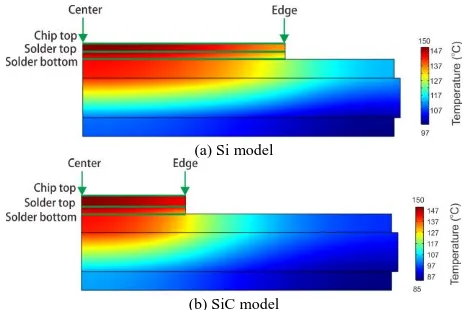
The temperature distribution for both Si and SiC models, coincident with the instant when the maximum junction temperature Tj,MAXis reached on the models are shown in Fig.
[image:7.612.317.561.86.408.2]10. The chip, die-attach and part of the copper of the DBC under the chip suffer higher thermal fatigue than the bottom of the DBC. This indicates that the fast power cycling mainly stresses the die-attach solder layer instead of the baseplate solder layer.
Fig. 7. The lifetime results of Si modules in Tj,mean=90˚C power cycling tests
and simulation
TABLEV
SIC&SICHIPMATERIALPARAMETERS
Parameters Si Chip SiC chip
Area
(mm x mm) 6.5 x 6.8 3.1 x 3.36 Thickness (μm) 140 180
CTE
(10-6/K) 3 3.4
Young’s Modulus (GPa) 162 501 Poisson’s Ratio (1) 0.28 0.45 Thermal Conductivity (W/(m x K)) 130 370 Thermal Capacity (J/(kg x K)) 700 690
[image:7.612.75.279.180.312.2]According to (3), the temperature swing determines the fatigue stress caused by CTE mismatch and the high temperature can lead to more stresses on the die-attach. By using this power cycling condition and boundary conditions the models are suitable to be used to evaluate the mechanical fatigue of die-attach solder layer.
The temperature distributions on these stressed parts of the model are as shown in Fig. 11 for the top surface of the chip, interface of die/solder and the interface of solder/DBC copper. The distance is the position on each surface to the center of the model.
The temperature of the SiC and Si chip center is both 150˚C extracted as the junction temperature Tj. Considering a quarter
chip area and 2 times higher thermal conductivity of the SiC to give better heat dissipation performance as compared to Si, the temperature on the interface of both chip and solder in the SiC model is lower than those in the Si model. However, in the SiC model, the temperature on the edge of chip surface and the temperature on the edge of the solder top surface are both higher than those in the Si model.
In addition to the different temperature profiles on the solder and the dimensions of the chip, the different thermomechanical properties of the semiconductor material will cause different stresses on the solder, resulting in a different lifetime according to the models presented previously. The next section of this paper characterizes the stresses on the solder as a function of the semiconductor material and its implications on the lifetime
of the solder.
IV. STRESS AND LIFETIME COMPARISON
A. Stress comparison
The stress distribution of solder layer for both Si and SiC models will be analyzed in detail first. For a power cycle with Tj,mean=90˚C and ΔTj=120˚C, the creep strain and strain energy
density distribution on the edge of die-attach solder layer after 5 cycles are presented in Fig. 12.
For both semiconductor materials the accumulation of creep strain caused by the thermal-stress cycling is mainly concentrated in the interfacial corners of the solder layer, In the case of the Si chip, shown in Fig. 12(a) and Fig. 12(c), creep accumulation is observed in both the solder/die interface and the solder/DBC copper interface, however in the case of the SiC chip, the creep strain is mainly concentrated at the chip/die interface, as the simulations results in Fig. 12(b) and Fig. 12(d) shown. There is no noteworthy indication of creep strain or creep energy being accumulated at the solder/DBC copper layer interface when the SiC chip is used.
The creep strain and strain energy density along the boundary between the solder layer and chip are shown in Fig. 13, as a function to the distance to the edge.
[image:8.612.321.562.75.348.2]Both the creep strain and creep energy decrease towards the center of the chip. At the corner point, the creep strain and creep energy with SiC model solder are 29% and 31% higher than those with Si. The creep strain of SiC is larger than 0.005 within the distance of 0.1 mm, but the creep strain of Si remains 0.005 till the distance of 0.2 mm. Thus the creep strain and creep
Fig. 9.Power density cycle and resulting junction temperature profiles
(a) Si model
[image:8.612.52.289.129.251.2](b) SiC model
Fig. 10. Temperature distribution on the model at instant Tj,MAX is reached
(a) Chip top surface
[image:8.612.54.289.298.453.2](b) Solder layer interfaces
energy concentration is more significant in the SiC model causing an initial crack much more easily to grow from the edge of the solder layer.
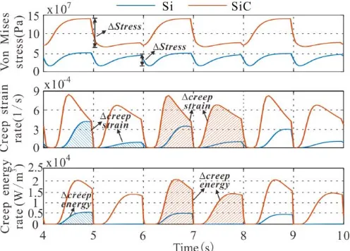
Analyzing the creep strain distributions presented in Fig. 12, the point of the solder subjected to higher strain is the corner of the solder/ chip interface, hence the evolution of the stress for this point should be monitored during the FE simulations. Considering the 3 power cycles defined in Fig. 9, the Von Mises
stress, creep strain rate and energy density at the selected point are presented in Fig. 14 for both semiconductor materials.
From the FE results, it can be observed that the transient response of temperature is the major cause of the thermomechanical stresses, generating higher Von Mises stress during the heating transient than during the cooling transient. The Von Mises stress is caused by the thermal expansion and the CTE mismatch between materials, and it fluctuates with the temperature during each cycle as explained by (2) and (3).
The creep strain rate and creep energy rate clearly show the different accumulating rate of creep strain and creep energy in the die-attach solder layer between Si and SiC. The accumulation value of creep strain and creep energy during one cycle – the area of the rate, which are the main factors of solder failure, can be used to evaluate the lifetime of the solder layer. Based on these the larger Young’s Modulus and higher thermal conductivity of SiC cause the creep strain and creep energy accumulated much faster in its die-attach solder than that in Si model during power cycling leading the SiC device more unreliable.
In the case of the SiC model, the corners of solder layer are subjected to cyclic stresses (70 MPa) 2.2 times as in the silicon model (32.1 MPa). The accumulated creep strain in the corner
(a)
(b)
(c)
[image:9.612.318.561.69.215.2](d)
Fig. 12. Creep strain distribution in the solder layer of (a) Si and (b) SiC,
Creep energy distribution in the solder layer of (c) Si and (d) SiC in the end
[image:9.612.65.275.92.611.2]of power cycling.
[image:9.612.314.562.262.440.2]Fig. 13. Creep strain and creep energy distribution on the die/ solder interface
of solder in SiC model during one cycle (5.85 x 10⁻⁴) is 2.5 times as that in the Si model (2.34 x 10⁻⁴). Assessing the fatigue accumulation of the solder layer by energy, it can be seen that the accumulated energy density of the solder layer of the SiC devices (15891 J/m3) is about 3.6 times as the Si device (4459 J/m3) during the temperature cycling.
Therefore, the creep energy can generate serious fatigue damage in the SiC model compared with Si, and it could be used as a fatigue indicator for estimating the lifetime of the SiC device.
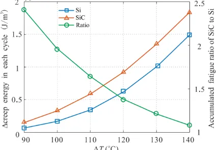
The Si and SiC solder layer accumulated creep energies (defined in Fig. 14) are extracted from FE models at junction temperature excursions Tj ranging from 90 to 140˚C as shown
in Fig. 15. Due to the higher Young’s modulus and larger thermal conductivity of SiC the creep energy of SiC die-attach solder maintaining at a higher level than Si among all of these cycling conditions. The creep energy of SiC under ΔTj=90 ˚C is 2.4 times compared with Si while the fatigue ratio keeps reducing to 1.2 suggesting the fatigue of SiC and Si will be close under high temperature swings. It also can be inferred that the difference of lifetime between SiC and Si at lowerTj
would be significant.
B. Lifetime Comparison
The FE results presented in the previous section shown that, for the same junction temperature profile, the creep energy and creep strain are higher when a SiC chip is used. This higher creep energy can generate serious fatigue damage in the solder, leading to a reduced lifetime of the solder.
Morrow’s model, used in section II for the evaluation of the lifetime of the solder for a Si chip, is based on the creep energy. Based on that model, the lifetime distribution across evaluated part of the solder layer can be calculated using the FE results for both Si and SiC chips. Using the creep energy distribution for a with Tj,mean=90˚C and ΔTj=120˚C cycle, shown in Fig. 12,
the estimated number of cycles to failure for both chip materials and the same solder are shown in Fig. 16.
Consistent with theoretical analysis, the creep energy density distribution demonstrates that the solder layer of the SiC device has more significant fatigue effect, and the upper corner of the solder layer corresponds to the shortest lifetime. The higher
concentrated stresses on the solder when the SiC is used suggest a higher probability of crack initiation, hence a reduced lifetime of the solder.
Using the validated model, the lifetime of the solder can be evaluated using the stresses on the solder when a SiC chip is used. The lifetime criterion of accelerated aging experiment is 20% thermal resistance increase corresponding to 23% crack length in solder layer in the FE model. For a mean junction temperature Tj,mean=90C and range of junction temperature
excursions Tj from 90 to 140C the predicted lifetimes for both
semiconductor materials are shown in Fig. 17.
[image:10.612.321.561.88.356.2]Due to the higher Young’s modulus of SiC, the lifetime of SiC die-attach solder is always at the lower level in all of the cycling conditions as shown in Fig. 17. The stress level of SiC under minor temperature excursions, which are more common
Fig. 15. Result of solder layer fatigue in SiC and Si
(a) edge of Si die-attach
(b) edge of SiC die-attach
[image:10.612.65.278.177.324.2]Fig. 16. Solder layer corner lifetime in Si and SiC devices
[image:10.612.329.563.492.646.2]in normal operation, is still higher than Si leading to the difference of lifetime between SiC and Si at lowerTj would
be more significant. Fig. 17 also plots the ratio of the lifetimes predicted for the SiC and Si devices for each Tj while Tj,mean is
kept at 90C, where it can be observed the SiC lifetime is quadratically correlated to Si under the same temperature profile. For ΔTj=90⁰C, the lifetime of the SiC device is only
60% of that of the Si device; but as the temperature swing increases, the lifetime of SiC and Si eventually become similar with the ratio approaching 1.
V. CONCLUSIONS
This paper presents a comparative study on the fatigue stresses in a Si and a SiC power device (module). Due to the higher Young’s Modulus of SiC material, the solder layer in a SiC module experiences higher fatigue stresses than in a Si module for the same junction temperature profile. This is the case even the SiC die-size is smaller for the same current and voltage ratings. The FE model was firstly performed for the Si device and validated using power cycling tests for the same Tj,mean and Tj as to be later used for SiC. Then the evaluation
method for reliability of the same solder material was extrapolated for the SiC device to estimate the lifetime of solder layer without the need of power cycling test for SiC devices. From the FE analysis the thermomechanical stresses of a SiC device can be significantly higher than those of the comparative Si device under the same junction temperature profile, particularly for lower Tj values. This also leads to the
predicted lifetime of a SiC device to be potentially considerably lower than that of the Si device (only 60% of Si device at Tj
90˚C). This finding may help to justify the necessity of new packaging technologies for SiC devices. An intended contribution of this study is that the large volume of available lifetime test data for Si power modules can then provide useful references to converter designers who are considering to include SiC devices in their systems.
REFERENCE
[1] J. Lutz and R. Baburske, “Some aspects on ruggedness of SiC power devices,” Microelectronics Reliability, vol. 54, no. 1, pp. 49-56, Jan. 2014.
[2] R. Singh, “Reliability and performance limitations in SiC power devices,” Microelectronics Reliability, vol. 46, no. 5, pp. 713-730, Jun. 2006.
[3] A. Agarwal, H. Fatima, S. Haney and S. H. Ryu, “A new degradation mechanism in high-voltage SiC power MOSFETs,” IEEE Electron Device Letters, vol. 28, no. 7, pp. 587-589, Jul. 2007.
[4] J. A. Schrock, W.B. Ray, K. Lawson, A. Bilbao, S. B. Bayne, S. L. Holt L. Cheng, J. W. Palmour and C. Scozzie, “High-mobility stable 1200V, 150A 4H-SiC DMOSFET long-term reliability analysis under high current density transient conditions,” IEEE Transactions on Power Electronics, vol. 30, no. 6, pp. 2891-2895, Jun. 2014.
[5] A. Tanaka, S. Ogata, T. Izumi, K. Nakayama, T. Hayashi, Y. Miyanagi and K. Asano, “Reliability investigation of SiC bipolar device module in long time inverter operation,” in 2012 24th International Symposium on Power Semiconductor Devices and ICs (ISPSD), pp. 233-236, Jun. 2012. [6] H. Matsunami and T. Kimoto, “Step-controlled epitaxial growth of SiC: high quality homoepitaxy,” Materials Science and Engineering: R: Reports, vol. 20, no. 3, pp. 125-166, Aug. 1997.
[7] L. C. Yu, G. T. Dunne, K. S. Matocha, K. P. Cheung, J. S. Suehle and K. Sheng, “Reliability issues of SiC MOSFETs: a technology for
high-temperature environments,” IEEE Transactions on Device & Materials Reliability, vol. 10, no. 4, pp. 418-426, Dec. 2011.
[8] M. Ciappa, “Selected failure mechanisms of modern power modules,”
Microelectronics Reliability, vol. 42, no. 4, pp. 653-667, May. 2002. [9] C. Herold, M. Schaefer, F. Sauerland, T. Poller, J. Lutz and O. Schilling,
“Power cycling capability of modules with SiC-diodes,” in International Conference on Integrated Power Systems, pp. 1-6, Feb. 2014.
[10] S. Liebig and J. Lutz, “Efficiency and lifetime of an active power filter with SiC-MOSFETs for aerospace application”, PCIM Europe, pp. 1-9, May. 2014.
[11] S. Liebig, A. Engler and J. Lutz, “Design and evaluation of state of the art rectifiers dedicated for a 46 kW E-ECS aerospace application with respect to power density and reliability”, in Proceedings of the 2011-4th
European Conference on Power Electronics and Applications (EPE 2011), pp. 1-10, Aug. 2011.
[12] T. Herrmann, M. Feller, J. Lutz, R. Bayerer and T. Licht, “Power cycling induced failure mechanisms in solder layers”, in Proc. Eur. Conf. Power Electron. Appl, pp. 1-7, Sep. 2007.
[13] B. Ji, X. Song, E. Sciberras, W. Cao, Y. Hu and V. Pickert, “Multiobjective design optimization of IGBT power modules considering power cycling and thermal cycling”, IEEE Transactions on Power Electronics, vol. 30, no. 5, Sep. 2015.
[14] W. Lai, M. Chen, L. Ran, O. Alatise, S. Xu and P. Mawby, “Low ΔTj stress cycle effect in IGBT power module die-attach lifetime modeling,”
IEEE Transactions on Power Electronics, vol. 31, no. 9, pp. 6575-6586, Sep. 2016.
[15] W. W. Lee, L. T. Nguyen and G. S. Selvaduray, “Solder joint fatigue models: review and applicability to chip scale packages,”
Microelectronics reliability, vol. 40, no. 2, pp.231-244, 2000.
[16] I. Kim and S. B. Lee, “Reliability and failure analysis of lead-free solder joints for PBGA package under a cyclic bending load,” IEEE Transactions on components and packaging technologies, vol. 31, no. 2, pp. 478-484, 2008.
[17] F. P. Mccluskey, M. Dash, Z. Wang and D. Huff, “Reliability of high temperature solder alternatives,” Microelectronics Reliability, vol. 46, no. 9-11, pp. 1910-1914, Nov. 2006.
[18] J. A. Dicarlo, “Creep of chemically vapour deposited SiC fibres,”
Journal of Materials Science, vol. 21, no. 21, pp. 217-224, Jan. 1986. [19] S. Zhu, M. Mizuno, Y. Kagawa, J. Cao, Y. Nagano and H. Kaya, “Creep
and fatigue behavior of SiC fiber reinforced SiC composite at high temperatures,” Materials Science & Engineering A, vol. 225, no. 1, pp. 69-77, Apr. 1997.
[20] L. Navarro, X. Perpina, P. Godignon, J. Montserrat, V. Banu, M. Vellvehi and X. Jorda, “Thermomechanical assessment of die-attach materials for wide bandgap semiconductor devices and harsh environment applications,” IEEE Transactions on Power Electronics, vol. 29, no. 5, pp. 2261-2271, May. 2014.
[21] A. Ibrahim and Z. Khatir, “Power cycling ageing tests at 200°C of SiC assemblies for high temperature electronics,” in Power Electronics and Applications, 2013 15th European Conference on, pp. 1-10, Sep. 2013. [22] Y. Wang, X. Dai, G. Liu, Y. Wu, D. Li and S. Jones, “Status and trend
of SiC power semiconductor packaging,” in Electronic Packaging Technology (ICEPT), 2015 16th International Conference on, pp. 396-402, Aug. 2015.
[23] F. Lang, Y. Hayashi, H. Nakagawa, M. Aoyagi and H. Ohashi, “Joint reliability of double-side packaged SiC power devices to a DBC substrate with high temperature solders,” in Electronics Packaging Technology Conference (2008 EPTC), pp. 897-902, Dec. 2008. [24] J. G. Bai and G. Q. Lu, “Thermomechanical reliability of
low-temperature sintered silver die attached SiC power device assembly,”
IEEE Transactions on Device & Materials Reliability, vol. 6, no. 3, pp. 436-441, Sep. 2006.
[25] J. G. Bai, J. Yin, Z. Zhang, G. Q. Lu and J. D. van Wyk, “High-temperature operation of SiC power devices by low-“High-temperature sintered silver die-attachment,” IEEE Transactions on Advanced Packaging, vol. 30, no. 3, pp. 506-510, Aug. 2006.
[26] J. Li, I. Yaqub, M. Corfield, P. Agyakwa and C. M. Johnson, “Comparison of thermo-mechanical reliability of high-temperature bonding materials for attachment of SiC devices,” in Integrated Power Systems (CIPS), 2014 8th International Conference on, pp. 1-7, Feb. 2014.
http://www.rogerscorp.com/documents/3009/pes/curamik/curamik-Ceramic-Substrates-Product-Information.pdf
[29] K. C. Otiaba, M. I. Okereke and R. S. Bhatti, “Numerical assessment of the effect of void morphology on thermo-mechanical performance of solder thermal interface material,” Applied Thermal Engineering, vol.64. no.2,pp. 51-63, Mar. 2014.
[30] B. Ji, X. Song, W. Cao, V. Pickert and Y. Hu, “In situ diagnostics and prognostics of solder fatigue in IGBT modules for electric vehicle drives,” IEEE Transactions on Power Electronics, vol. 30, no. 3, pp. 1535-1543, Mar. 2015.
[31] L. Zhang, J. G. Han, Y. H. Guo and C. W. He, “Effect of rare earth Ce on the fatigue life of SnAgCu solder joints in WLCSP device using FEM and experiments,” Materials Science and Engineering: A, vol. 597, pp.219-224, Mar, 2014.
[32] J. W. McPherson, Reliability physics and engineering: time-to-failure modeling, Springer Science & Business Media, 2010.
[33] B. Gao, F. Yang, M. Chen, L. Ran, I. Ullah, S. Xu and P. Mawby, “A temperature gradient based condition estimation method for IGBT module,” IEEE Transactions on Power Electronics, vol. 32, no. 3, pp. 2227-2242, Mar. 2017.
[34] C. Busca, R. Teodorescu, F. Blaabjerg, S. Munk-Nielsen, L. Helle, T. Abeyasekera and P. Rodriguez, “An overview of the reliability prediction related aspects of high power IGBTs in wind power applications,” Microelectronics Reliability, vol. 51, no. 9, pp. 1903-1907, Nov. 2011.
[35] J. H. L. Pang, B. S. Xiong and T. H. Low, “Low cycle fatigue models for lead-free solders,” Thin Solid Films, vol. 462, pp. 408-412, Sep. 2004. [36] J. H. Pang, B. S. Xiong and T. H. Low, “Creep and fatigue
characterization of lead free 95.5 Sn-3.8 Ag-0.7 Cu solder,” in
Proceedings Electronic Components and Technology Conference 54th, 2004, pp. 1333-1337.
[37] H. Huang and P. A. Mawby, “A lifetime estimation technique for voltage source inverters,” IEEE Transactions on Power Electronics, vol. 28, no. 8, pp. 4113-4119, Aug, 2013.