Influence of nanoscale surface roughness
on flow behaviour in fluidic
microchannels
Master thesis report
An Gao
Master program of Nanotechnology
University of Twente
Transducers Science and Technology (TST) Group
Twente University
Drienerlolaan 5
7522 NB Enschede
The Netherlands
The MSc committee consists of:
Chairman: Prof. Dr. Miko Elwenspoek
Supervisor: Dr. Ir. H. V. Jansen
Daily Supervisor: Dr. Ir. Sandeep Unnikrishnan
Microsieve is largely used in the area of filtration and selective gas permeation. Such applications can benefit from a microsieve with a low flow resistance. The flow resistance is usually achieved by reducing the thickness of the microsieve, however, at the mean time microsieve membrane strength becomes low. To solve this dilemma, a microsieve has to be thick enough to withstand high pressure or forces while at the same keep its resistance remaining the same as a very thin membrane. The conductance difference for thick and thin microsieve membranes is caused by the rough surface of microsieve channel. Therefore, it is postulated that a microsieve with extremely smooth channel surface would prevent the influence on total resistance from the channel wall roughness.
A silicon microsieve with smooth channel surface is designed and fabricated to examine the influence of surface roughness on flow conductance. DRIE is applied to drill holes through the wafer, which will create microscale roughness. The circular holes will be getting a post processing with KOH wet etching: a rhombus shaped channel is fabricated with smooth surface. By measuring the flux through the microsieve with nanoscale roughness and comparing this with the microsieve with micro roughness, the influence of surface roughness on flow flux or flow conductance is determined.
Content
Chapter 1 Introduction ... 1
1.1 Micro-mechanical electrical systems ... 1
1.2 Problem statement ... 2
1.3 Outline ... 2
Reference:... 3
Chapter 2 Theory: Gas flow conductance in capillary ... 4
2.1 Knudsen Number... 4
2.2 Flow conductance in viscous regime ... 5
2.3 Slip flow and Interaction between molecules and wall ... 7
Reference:... 10
Chapter 3 Microfabrication techniques ... 11
3.1 Wet chemical anisotropic etching ... 11
3.1.1 Silicon crystal structure ... 11
3.1.2 KOH etching ... 13
3.1.3 {111} planes related orientation dependent etching ... 16
3.2 High aspect ratio DRIE with profile control ... 19
3.2.1 The principle of plasma etching ... 19
3.2.2 Deep reactive ion etching (DRIE) ... 21
3.2.3 High aspect ratio trench etching ... 23
3.2.4 Equipment ... 24
3.3 Surface roughness reduction ... 25
3.3.1 KOH treatment ... 26
3.3.2 Hydrogen annealing ... 26
Reference:... 29
Chapter 4 Microsieve fabrication process ... 31
4.1 Mask design... 31
4.2 Process Outline ... 31
Chapter 5 Microsieve fabrication results and discussions ... 34
5.1 Lithography with SU 8 mask ... 34
5.2 DRIE with 908-35 mask ... 36
5.6 Conclusion ... 55
Reference:... 55
Chapter 6 Characterization ... 56
6.1 Glass tube bonding ... 56
6.2 Theoretical estimation of mass flow through microsieve ... 57
6.3 Flow measurement setup ... 60
6.4 Procedure of measurement ... 60
6.5 Experiment results and discussion ... 61
6.6 Discussions ... 66
Reference:... 69
Chapter 7 Conclusion and Future scope... 70
7.1 Overall conclusion... 70
7.2 Future scope ... 70
Acknowledgement ... 72
1
Chapter 1 Introduction
1.1 Micro-mechanical electrical systems
Microelectromechanical systems (MEMS) refer to devices that have characteristic length of less than 1 mm but more than 1 micron. MEMS combining electrical and mechanical components are fabricated using the process in the microelectronics industry, which is also called micromachining. The fabrication technologies include the lithography, wet etching (KOH, TMAH), dry etching (RIE, DRIE), deposition (LPCVD, PECVD) and other technologies capable of manufacturing small devices. Silicon is the most common use material in MEMS. It can be chemically etched into various shapes, and associated thin-film materials as polysilicon, silicon nitride and aluminum can be micromachined in batches into a vast variety of mechanical shapes and configurations. Nanodevices (some say NEMS) further push the envelope of electromechanical miniaturization.
MEMS are finding increased applications in a variety of industrial and medical fields, with a potential worldwide market in the billions of dollars. Accelerometers for automobile airbags, keyless entry systems, dense arrays of micromirrors for high-definition optical displays, scanning electron microscope tips to image single atoms, micro-heat-exchangers for cooling of electronic circuits, reactors for separating biological cells, blood analyzers and pressure sensors for catheter tips are a few of current usage. Microducts are used in infrared detectors, diode lasers, miniature gas chromatographs and high frequency fluidic control systems. Micropumps are used for ink jet printing, environmental testing and electronic cooling. Potential medical applications for small pumps include controlled delivery and monitoring of minute amount of medication, manufacturing of nanoliters of chemicals and development of artificial pancreas.[1]
There has been great interest in microfluidic devices during the last few decades in various research fields such as instrumentation and medical application. Microsieve is largely used in the area of filtration and selective gas permeation. With a functionalised coating, microsieve can become bio compatible and thus it can be used for medical application in hospitals.
2
1.2 Problem statement
As discussed above, high fluxes (high conductance) through the microsieve membrane require the membrane thickness to be extremely low, while on the other hand, the microsieve membrane strength is getting low because it is directly proportional to the thickness of microsieve[3]. This always causes a dilemma situation to us. One solution is to apply a specifically designed strong support underneath, but this will cause extra fabrication effort. Another solution is to make a microsieve thick enough to withstand high pressure or forces while at the same keep its resistance remaining the same as a very thin membrane. The conductance difference for thick and thin microsieve membranes is caused by the rough surface of microsieve channel. Therefore, it is postulated that a microsieve with extremely smooth channel surface would prevent the influence on total resistance from the channel wall roughness.
A silicon microsieve with smooth channel surface is designed and fabricated to examine the influence of surface roughness on flow conductance. DRIE is applied to drill holes through the wafer, which will create microscale roughness. The circular holes will be getting a post processing with KOH wet etching: a rhombus shaped channel is fabricated with smooth surface. By measuring the flux through the microsieve with nanoscale roughness and comparing this with the microsieve with micro roughness, the influence of surface roughness on flow flux or flow conductance is determined.
1.3 Outline
This report is focusing on the fabrication of a microsieve with smooth channel surface. After fabrication, gas flow through the microsieve is measured to examine the influence of surface roughness on flow conductance. The content of this report is arranged as follows:
Chapter 2 Theory: Gas flow conductance in capillary. In this chapter, a detailed discussion about gas flow conductance through capillary and microsieve is given in the viscous regime. Influence of gas molecule and solid interface interaction on determining the flow conductance is analyzed as well.
Chapter 3 Microfabrication techniques. In this chapter, important micromaching techniques deep reactive ion etching and KOH wet anisotropic etching are introduced. Surface roughness reduction methods are given at the last of the chapter: KOH etching, hydrogen annealing and sacrificial thermal oxidation.
Chapter 4 Microsieve fabrication process. In this chapter, a brief description of experiment is given, including process outline all the equipment used.
3 Chapter 6 Characterization. In order to measure the mass flow through the microsieve, it is firstly bonded to the glass tube then measured in home-made flow measurement system. The experiment results are compared with the theoretical results according to the formulas in Chapter2.
Chapter 7 Conclusion and Outlook. In this chapter, an overall conclusion is given for this master thesis project. And future work to improve this experiment is also discussed.
Reference:
1. Lennart Lofdahl, Mohamed Gad-el-Hak ―MEMS applications in turbulence and ßow control” Progress in Aerospace Sciences 35 (1999) 101-203
2. C.J.M van Rijn, M.C. Elwenspoek ―Microfiltration membrane sieve with silicon micro machining for industrial and biomedical applications‖ IEEE (1995) 83-87
3. Kuiper, S. ―Development and application of microsieves‖ PhD thesis, university of twente 2001.
4
Chapter 2 Theory: Gas flow conductance in capillary
In this chapter, firstly the three flow regimes are described and flow conductance in viscous regime is introduced. In the following, slip effect and gas-solid interaction are discussed. Finally, different kinds of silicon surface are analyzed.
2.1 Knudsen Number
The principle parameter in gas flow conductance theory is the Knudsen number (Kn), which distinguishes the different flow regimes. The Knudsen number is defined as the ratio of mean free path λ over by the characteristic dimension of the gas flow d, i.e., the capillary diameter when gas flow through a long capillary.
𝐾𝑛 =𝑑𝜆 (2.1)
[image:10.612.96.516.268.378.2]Considering the value of the Knudsen number, we can divide the gas flow into three regimes (Figure 2.1): viscous, transition and free-molecular flow. In the viscous flow regime (Kn < 0.01), the mean free path is small compared to the characteristic dimension of the channel, the collisions between molecules occur more frequently than collisions of molecules with the channel walls. Consequently, intermolecular collisions predominate in determining the characteristics of the flow. The flow in this regime is treated as a continuous medium. In the free-molecular or Knudsen Flow regime (Kn > 1), the mean free path is very large compared to the characteristic length scale and the intermolecular collision probability is quite low. The flow is limited by the collisions with the walls of the channel. In the transition flow regime (0.01 < Kn < 1), both types of collisions (intermolecular collision and collision with channel wall) are influential in determining the flow characteristics. There are only empirical equations to describe flow behavior in this regime. This division of the regimes of flow is very important because the methods used for calculation of the gas flows essentially depends on the regime. To calculate the Knudsen number, we have to know the mean free path, which absolutely cannot be measured directly. Therefore, we have to use the following formula to calculate the mean free path [2]:
𝜆 = 𝑘𝑇
2𝜋𝑑𝑚𝑜𝑙2 𝑃
(2.2)
Where the k is the Boltzmann constant and dmol is the diameter of the gas molecule. For most
gases, the mean-free-path at atmospheric pressure and room temperature is around 50-100nm.
Kn<0.01 0.01<Kn<1 Kn>1
Figure 2.1 flow regimes according to different Kn[2]
5
2.2 Flow conductance in viscous regime
In this viscous flow regime, the flow is described by the famous Hagen-Poiseuille`s law [3] (Eq.2.3) which was formulated in 1840 by observation of human blood flow in vessels and water flow in tiny tubes. This law describes the slow viscous incompressible flow through a constant circular cross-section. Poiseuille`s experiment gave the evidence to the correct boundary condition (no slip) for a laminar incompressible flow at a solid boundary. Hagen-Poiseuille`s law can be used to model the biological flow, such as blood flow and flow through the endothelial layer. It can also be used in porous media and filters.
𝑄𝑣𝑜𝑙 −𝑣𝑖𝑠−𝑡𝑢𝑏𝑒 =
𝜋𝑟4
8𝜂𝐿∗ ∆𝑃 (2.3)
Where Qvol-vis-tube is the volumetric flow rate [m
3
/s], η is the dynamic viscosity [Pa*s],
ΔP=Pentrance-Pexit [Pa] the pressure drop across the tube, L the tube length [m], the r its radius [m]. We can adjust equation 2.3 to incorporate compressible flow by introducing the mass flow
Qmass=Q. The transformation is using the ideal gas law PV=NRT (with N the number of molecules and R the universal gas constant):
𝑄𝑣𝑖𝑠−𝑡𝑢𝑏𝑒 =
𝑃𝑎
𝑅𝑇∗ 𝜋𝑟4
8𝜂𝐿∗ ∆𝑃 (2.4)
Where Qvis-tubeis the mass flow rate [mol/s], Pa=(Pentrance+Pexit)/2 the arithmetic mean pressure. Electricity was originally understood to be a kind of fluid. Both Poiseuille`s law and Ohm`s law illustrate the transport phenomena. Therefore, the flow conductance can be derived by analogy with electrically resistance. Poiseuille's law corresponds to Ohm's law for electrical circuits (∆V = I*R), where the pressure drop ΔP is analogous to the voltage ∆V and flow rate Q is analogous to the current I. Then the flow resistance or its reciprocal flow conductance is:
𝐹𝑣𝑖𝑠 −𝑡𝑢 𝑏𝑒 =
1 𝑅= 𝑄 ∆𝑃= 𝑃𝑎 𝑅𝑇∗ 𝜋𝑟4
8𝜂𝐿 (2.5)
The Hagen-Poiseuille`s law is based on some assumptions: The gas flow is laminar and is fully developed——thus the flow velocity profile is constant through the tube length, which means ignorance of the entrance and exit effect. Besides, the flow velocity at the wall is assumed to be zero, thus non-slip. In 1891, Sampson [4] solved the Stoke`s stream function for the viscous flux through a circular hole in a very thin wall with the assumption of zero velocity at the wall (eq.2.5&2.6).
𝑄𝑣𝑖𝑠−𝑜𝑟𝑖𝑓𝑖𝑐𝑒 =
𝑃𝑎
𝑅𝑇∗ 𝑟3
3𝜂∗ ∆𝑃 (2.6)
𝐹𝑣𝑖𝑠 −𝑜𝑟𝑖𝑓𝑖 𝑐𝑒 =
𝑃𝑎
𝑅𝑇∗ 𝑟3
6
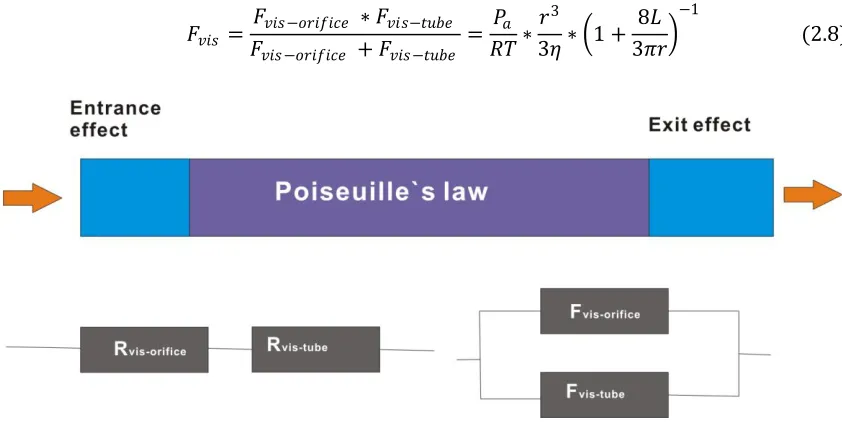
Now, we consider the gas flow through a tube with arbitrary length. In figure 2.2, there are actually two parts which contribute to the total flow transport, Poiseuille`s and Sampon`s flow. Therefore, the resistance from these two contributions is in series (conductance in parallel). The total flow conductance can be considered as addition of these two conductances. A general formula for conductance through tubes with arbitrary length in viscous regime is given [5]:
𝐹𝑣𝑖𝑠 =
𝐹𝑣𝑖𝑠−𝑜𝑟𝑖𝑓𝑖𝑐𝑒 ∗ 𝐹𝑣𝑖𝑠−𝑡𝑢𝑏𝑒
𝐹𝑣𝑖𝑠 −𝑜𝑟𝑖𝑓𝑖𝑐𝑒 + 𝐹𝑣𝑖𝑠−𝑡𝑢𝑏𝑒
= 𝑃𝑎 𝑅𝑇∗
𝑟3 3𝜂∗ 1 +
8𝐿 3𝜋𝑟
−1
(2.8)
When the single orifice or tube is replaced by a microsieve with a hexagonal array of orifices or tubes, the total transport can be simply add all contributions from the individual orifice or tube. However, the entrance and exit flow of a single orifice or tube will influence flow through its neighbouring ones. This influence is caused by the movement of molecules on the microsieve surface. This influence on the flow flux rate is corrected by Tio and Sadhal [6] with a correction factor(1 − 𝑓(𝑘))−1, and f(k)is given in eq. 2.9 with k the porosity of the microsive:
𝑓 𝑘 = 2𝐻3
3𝜋52(
3 2 𝑘)
3
2+ 6𝐻5
5𝜋72(
3 2 𝑘)
5
2+18𝐻7
7𝜋92(
3 2 𝑘)
7
2+ 56𝐻9
9𝜋11 2
3
2 𝑘
9 2……
(2.9)
The numerical values of the various Hiare: H3=11.0342, H5=6.76190, H7=6.19524, H9=6.05695.
Therefore, for a microsieve with hexagonal arrays of orifices, using the summation of individual orifice concept, the flow conductance can be given:
𝐹𝑣𝑖𝑠 −𝑜𝑟𝑖𝑓𝑖𝑐𝑒 −𝑠𝑖𝑒𝑣𝑒 = 𝐹𝑣𝑖𝑠−𝑜𝑟𝑖𝑓𝑖𝑐𝑒 ∗
𝐴𝑘
𝜋𝑟2∗ 1 − 𝑓 𝑘 −1
= 𝐴𝑟𝑘𝑃𝑎
3𝜂𝜋𝑅𝑇∗ 1 − 𝑓 𝑘
−1
(2.10)
Where A is the effective area of the microsieve and k is the porosity of the microsieve. Similarly, for for a microsieve with hexagonal arrays of tubes: the conductance is given:
Figure 2.2 Top: schematic of total flow consist of sampon`s effect and poiseuille`s law. Bottom: resistance series
[image:12.612.98.519.159.370.2]7 𝐹𝑣𝑖𝑠 −𝑡𝑢𝑣𝑒 −𝑠𝑖𝑒𝑣𝑒 =
𝐴𝑟𝑘𝑃𝑎
3𝜂𝜋𝑅𝑇∗ 1 − 𝑓(𝑘) + 8𝐿 3𝜋𝑟
−1
(2.11)
It is noticed that the viscous mass flow is direct proportional to the mean pressure and differential pressure. For the flow conductance in the molecular and transition regime, see appendix A&B.
2.3 Slip flow and Interaction between molecules and wall
The Hagen-poseuille`s law is based on the boundary condition of zero velocity (non-slip) at the wall surface. However, researches [7] show that there exists a non-zero velocity (slip) at the wall surface. The slip effect becomes very important for the micro/nano-scale flows as the characteristic length decreases.
In 1879, Maxwell studied the interaction at gas-solid interface and proposed a slip model for gases over a solid interface based on kinetic theory [8]. In 1909 Knudsen did the first experiment and confirmed the Maxwell slip model [1]. In the following decades the Maxwell model was demonstrated to be valid for gases over solid surfaces by the Boltzmann transport theory [9-11] and experimental measurements [12-15]. The Maxwell model has been widely used in rarefied gas dynamics and gas microfluidics.
In Maxwell`s theory of gas molecules interaction with solid surface, there are two models of gas molecule reflection: specular and diffuse (figure 2.3). The specular reflection model assumes that the incident molecules reflect on the body surface as the elastic spheres reflect on the entirely elastic surface, i.e., the normal to the surface component of the relative velocity reverses its direction while the parallel to the surface components remain unchanged. The diffusive reflection model assumes that the gas molecules strike the surface and are reflected in all directions with equal probability.
For a normal surface, Maxwell considered treating the surface as something intermediate between a perfectly specularly reflecting (specular) and perfectly diffusively reflecting surface. He assumed that in every unit of the surface, a portion of f diffusively reflects the incident molecules, while 1-f portion specularly reflects the incident molecules. It is clear that if all the molecules are
8
reflected diffusively, f=1, while if all the molecules are reflected specularly, f=0. It is frequently assumed in theoretical and numerical works that the gas is fully diffusively reflected at the wall (i.e., f=1).
In practice, the diffuse model (fully accommodation f=1) is applicable. The surfaces processed by usual industrial means at normal atmospheric temperature and with not too high incident energy of the oncoming flow, the diffuse reflection model can serve as fairly good approximation of the interaction of molecules with the body surface. Some people explain diffuse reflection as that the gas molecules are adsorbed near the wall for a certain time and totally forget the incident information. Thus, they will leave the wall and re-emitted to the free space above the wall in all angles [7]. However, this explanation is lack of evidence for how long the ―certain time” is and why would the gas molecules be absorbed. And if this is true, then specular reflection cannot exist. Because even for a perfectly flat surface, the incoming gas molecules into the surface will be adsorbed rather than directly reflected. In this report, we guess it is the roughness which probably causes the diffusive reflection (Figure 2.4). Five molecules strike the surface in a parallel direction. But they meet the surface in the different orientation with respect to the normal direction of the meeting point on the surface. As a result, when the molecules are reflected from
the surface, they will scatter in different directions. Therefore, we postulate that, if the surface roughness is largely reduced, fewer molecules will be reflected diffusively, and on the other hand, more gas molecules will be reflected specularly from the surface. This hypothesis will be tested in the following experiment of this report.
9 For a validation of our hypothesis, an experiment is designed in Chapter 4. Silicon is employed as the surface material, because it is convenient to make devices with silicon due to its high developed micromachining techniques. Before going to the experiment, an inside view of silicon surface made by different techniques is discussed in below.
In figure 2.5, it is shown a rough surface fabricated by using DRIE technique. Due to the larger scale roughness on the surface fabricated by DRIE, the surface will produce diffusive reflection. After a KOH treatment, the surface roughness can be largely reduced to the nano scale.
As discussed above, the surface roughness might play an important role in flow bahivor through tubes. To eliminate the influence from the surface roughness, one way is to make the tubes extremely thin, e.g., a thin orifice. Because the length of orifice is so short and even shorter than the mean free path of the gas molecules, gas molecules will directly go through the orifice without any collision with the walls. Experiment is done by Uniniksrishnan et al [16] in this group: an ultra-thin (45nm) nanosieve is used to examine the flow behavior at different pressures (thus different flow regime). Experiment results show that conductance in transition regime is the superimposition of viscous and molecular flow fluxes due to absence of gas-wall collisions. In this report, another method is proposed. Instead of making the tube extremely short, we try to make extremely smooth (ideally atomically smooth) channel surface for a microsieve. If most of the gas molecules are reflected specularly from this smooth surface as what we postulated, the channel wall has no contribution to total resistance or conductance, because there is no momentum loss along the motion direction during the gas molecule-wall collisions. Therefore, conductance for a tube or a microsieve is independent of its length, and is only related to the entrance and exit effect (just like an orifice). The formula for viscous flow conductance through a microsieve with atomically smooth surface is then reduced to:
𝐹𝑣𝑖𝑠 −𝑠𝑚𝑜𝑜𝑡 =
𝐴𝑟𝑘𝑃𝑎
3𝜂𝜋𝑅𝑇∗ 1 − 𝑓 𝐾
−1
(2.12)
10
The flow conductance is believed to be much larger than that for a microsieve with the same length but a relatively rough surface. The ratio of flow conductance for smooth and rough surface is written as:
𝐶 =𝐹𝑣𝑖𝑠−𝑠𝑚𝑜𝑜𝑡 𝐹𝑣𝑖𝑠 −𝑟𝑜𝑢𝑔
=
𝐴𝑟𝑘𝑃𝑎
3𝜂𝜋𝑅𝑇 ∗ 1 − 𝑓 𝐾
−1
𝐴𝑟𝑘𝑃𝑎
3𝜂𝜋𝑅𝑇 ∗ 1 − 𝑓(𝑘) + 8𝐿 3𝜋𝑟
−1=
1 − 𝑓(𝑘) +3𝜋𝑟8𝐿
1 − 𝑓 𝐾 = 1 +
8𝐿 3𝜋𝑟(1 − 𝑓 𝑘 )
(2.13)
Where f(k) is the correction factor. If we have a microsieve with aspect ratio (L/r) of 20, C is around 20 according to eq. 2.13(For the value of f(k), k is given at 43.67% in chapter 6 and f(k) is 0.885). Therefore, if our hypothesis is true, during the experiment, compared with that through microsieve with rough surface a much larger flow flux (or conductance) through the microsieve with smooth surface will be observed.
Later on, the experiment results will show this hypothesis is not correct due to lack of consideration on atomic roughness on the surface and gas molecule shape. More details will be given in Chapter 7.
Reference:
1. Kundsen M. 1909a Ann. Phys., Lpz. 28 75-130
2. Dushman, ―Scientific foundation of vacuum technique‖ 2nd John wiley&Sons Inc. 3. Eckhard M.S. Hitzer, ―Early works on the Hagen-Poiseuille flow‖, Mem. Fac. Eng. Fukui
Univ. 49(1), 45 (2001)
4. Sampson R A 1891, On Stokes's current function. Phil Trans R Soc A182, 449 5. Z. Dagan, S. Weinbaum and R. Pfeffer, Chem. Eng. Sci., 38 (1983) 583-596 6. Tio K and Sadhal 1994 Appl. Sci. Res. 52 1
7. Bing-Yang Cao, ―Molecular Momentum Transport at Fluid-Solid Interfaces in MEMS/NEMS: A Review‖, Int. J. Mol. Sci. 2009, 10, 4638-4706;
8. Maxwell, ―On Stresses in Rainfied Gases arising from Inequalities of Temperature‖, Philosophical Transactions of the Royal Society, Part I. 1879.
9. Schaaf, S.A.; Chambre, P.L. Flow of Rarefied Gases; Princeton University: New Jersey, NJ, USA, 1961.
10. Muntz, E.P. Rarefied-gas dynamics. Annu. Rev. Fluid Mech. 1989, 21, 287–417.
11. Cercignani, C. Rarefied Gas Dynamics: From Basic Concepts to Actual Calculations; Cambridge University Press: Cambridge, UK, 2000.
12. Millikan, R.A. Coefficients of slip in gases and the law of reflection of molecules from the surfaces of solids and liquids. Phys. Rev. 1923, 21, 217–238.
13. van Dyke, K.S. The coefficients of viscosity and of slip of air and of carbon dioxide by the rotating cylinder method. Phys. Rev. 1923, 21, 250–265.
14. Chiang, S.F. Drag Forces on Rotating Cylinders at Low Pressures, Ph.D. Thesis, University of California, US, 1952.Beams J.W.; Young III, J.L.; Moore. J.W. The production of high centrifugal fields. J. Appl. Phys.1946, 17, 886–890.
11
Chapter 3 Microfabrication techniques
In the micromachining techniques, etching is basically divided into two groups: wet chemical etching and dry (plasma) etching. Wet chemical etching was important technique for the integrate circuit manufacturing in 1960s. It can provide low cost and high selectivity between substrate and mask. Later on in the early 1970s, dry etching was widely adopted for anisotropic etching. It can offer the possibility of vertical etch rate which greatly exceeds the horizontal etch rate. From then on, more and more research came into dry or plasma etching. In this chapter, both of these two techniques will be discussed in detail. The first part is about wet chemical anisotropic etching. The principle of etching mechanism will be discussed here. Detailed discussion about KOH anisotropic etching is introduced as well. In the second part, a general introduction about dry plasma etching is given. Special discussion focuses on deep reactive ion etching, especially on Bosch process.
3.1 Wet chemical anisotropic etching
Wet chemical anisotropic etching is one of most important techniques for bulk silicon micromachining. The anisotropic feature of etching silicon allows us to precisely control the etching shape and dimensions of structures. This technique is commonly used for making pressure or acceleration sensors. Furthermore, some complicated 3D structures, such as ink-jet printing devices and other microfluidic systems, are also fabricated with this technique. The possibility of batch processing by using wet chemical etching could largely reduce the production cost, which makes devices more competitive on the market.
3.1.1 Silicon crystal structure
The anisotropy of silicon etching is dominated by the silicon planes. Therefore, before we discuss the etching mechanism, a general introduction of silicon crystal structure is given in the following [1].
A crystal structure is formed by placing a collection of atoms (also called basis) at each point of the lattice. The lattice is defined as the periodic arrangement of atoms, which can be described by three translational vectors, a, b, c, in 3-D structures. The arrangement of atoms in the crystal looks the same when viewed from the point r as when viewed from r` translated by an integral multiple of vector:
𝒓` = 𝒓 + 𝑢1𝒂 + 𝑢2𝒃 + 𝑢3𝒄 (3.1)
Here, the u1, u2, u3, are arbitrary integers. The lattice is called the primitive lattice if any two
12
There are three most common basic crystal structures: Simple Cubic, Body-centered cubic, and Face-centered cubic. They are shown in figure 3.1.
Silicon has a diamond crystal structure. The lattice of this structure is face-centered cubic, and the basis has two identical atoms at coordinates (000), (1/4,1/4,1/4) located at each point of the Face-Centered Cubic lattice, as shown in figure 3.2. From the figure, we can see that each atom has 4 nearest neighbors. The diamond structure is relatively empty: the volume filled by the hard spheres is only 34% of the total available volume.
Figure 3.1 three basic crystal structures
Figure 3.2 Left: atomic positions projected on the cube face in a cube of diamond structure. Fractions denote
13 Different planes or directions in the crystal are usually identified by a set of integers h, k, and l, which are also called Miller indices. For a specific crystal face, the Miller indices are given by (hkl) for the plane and [hkl] for the crystal orientation (vector perpendicular to the plane). Three fundamental planes are shown in silicon crystal structure in Figure 3.3.
The family of faces, like (100), (010), (001) are all equivalent and called {100} planes. Similarly, the direction [100], [010], [001] are marked as a set of <100> directions. Usually, in micromaching, <100> and <110> orientation wafers are the most two common used wafers.
3.1.2 KOH etching
KOH is the most commonly used etchant for wet chemical anisotropic etching. It is much less dangerous than other etchant, easy to prepare and etches fast. Although it is incompatible with IC industry due to the metal contamination, it is still can be used for industrial use in micromaching. The first detailed study of KOH etching was done by Price in 1973[3]. He used not only KOH solutions but also KOH+Isopropyl alcohol. He found the KOH solution at a concentration of 10%-15% (weight percent) had the fastest etch rate. When the isopropyl alcohol was added, the fastest etch rate occurred at a concentration of 30%. Roughly speaking, the addition of alcohol would decrease the etch rate. He also found that the etching was not diffusion limited because the solution stirring had no influence on the etch rate. On <100>silicon wafers, Price observed an etch ratio of 35:1 for {100}/ {111} crystal planes. Later on Kendall [4] reported that the etch rate of {110} crystal planes was at least 400 times faster than that on the {111} crystal planes using 44% concentration KOH solutions at 85oC. In his study, he also showed the relationship between the etch rate and the degree of crystal misalignment. His results were shown in Figure 3.4.
Figure 3.3 Top: fundamental planes in silicon crystal. Bottom: side view of silicon crystal structure of three
[image:19.612.92.513.150.377.2]14
The chemical reaction during the etching process was investigated by Palik[5,6,7]. He monitored the reaction process by Raman spectroscopy. It was pointed out in his study that both hydroxide (OH-) and wafer (H2O) were involved with the etching. He proposed a chemical reaction equation:
𝑆𝑖 + 2𝐻2𝑂 + 2𝑂𝐻−→ 𝑆𝑖(𝑂𝐻)2𝑂2−2+ 2𝐻2
In a later work, he took the energy level into consideration and said that the reaction transferred an electron form OH- into the silicon surface bond and then back to the etch products. However, Raley [8] et al assumed that there were four electrons which were transferred into the conduction band by an initial oxidation reaction and the electrons will be consumed in a following reduction step. His chemical reaction equations are:
𝑆𝑖 + 2𝑂𝐻−→ 𝑆𝑖(𝑂𝐻)
2+2+ 4𝑒−
𝑆𝑖(𝑂𝐻)2+2+ 4𝑒−+ 4𝐻2𝑂 → 𝑆𝑖(𝑂𝐻)6−2+ 2𝐻2
In order to find the etching rate of different crystal planes, Seidal [9] suggested a wagon wheel pattern mask (Shown in figure 3.5). When the {111} crystal planes meet at concave corners,
Figure 3.5 Left: wagon wheel pattern mask. Lateral underetch rates as a function of orientation when using a 50%
KOH solution at a temperature 78oC of <100> wafer (middle) and <110> wafer (right)[9].
Figure 3.4 Left: Disorientation θ between {110} and {111} planes. Right: The undercutting to depth ratio (etch rate
15 etching effectively stops. However, at the convex corners, the etch rate is quite fast and lateral undercut occurs. Corner compensation (adding mask materials to the convex corners) will slow down the etch rate at these corners.
16
3.1.3 {111} planes related orientation dependent etching
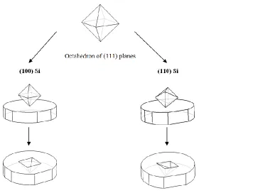
In the silicon crystal, eight {111} planes form an octahedron. The wafer orientation determines how the octahedron is located in the wafer with respect to the wafer flats. Different etching shapes can be achieved due to the restriction of very slow etch rate on {111} planes in KOH solutions. Figure 3.6 shows the octahedron of {111} planes and how it is located in the <100> and <110> wafers.
The most common applications are to fabricate V-groove and U-groove. To achieve this, a mask with a rectangular opening is used. For the V-groove on the <100> wafers (figure 3.7), the mask is aligned parallel to the prime flat of wafer. The etch proceeds downward until {111} planes are reached. In the V-groove, the {111} planes intersects with {100} planes at an angle of 54.7o.
[image:22.612.171.527.178.450.2]Figure 3.6 Position of the octahedron limited by {111} planes in differently oriented silicon wafers
17 However, the angle will slightly vary because the etch rate of {111} is not zero and the alignment of wafer surface and wafer flat is not perfect with crystal orientation. For a U-groove (Figure 3.8), the mask is aligned parallel to the prime flat. The etch process continues until the two {111} planes intersect with each other. The lateral etch is restricted by {111} planes.
One of the extensive applications of the octahedron feature of silicon crystal is to fabricate the rhombus shaped microchannel [10]. The cross-section of this octahedron with the (110) plane is a rhombus with interior angles of 70.53o and 109.47o. This rhombus is marked in Figure 3.9 in dotted lines. The octahedron is extended along the [110] direction, as shown in the Figure 3.9 in order to give a clear view.
However, a direct wet KOH etching of these channels is not possible because two {111} planes will lead to etch stop at the channel bottom. In order to etch through the limiting {111} planes, the crystal structure has to be damaged along the etch path. This usually can be done by laser beam or deep reactive ion etching. (Figure 3.10)
Figure 3.8 Left: mask alignment parallel to the prime flat. Right: U-groove with 90 {111} planes
18
With these techniques, various kinds of microchannels can be fabricated on wafers with different orientations (Figure3.11).
Figure 3.11 Schematic view of possible microchannels in silicon formed by intercepting the extended octahedron
with the surfaces of (a)<110> , (b) <110>, (c) <100>, and (d) <111> silicon wafers, respectively.[10]
Figure 3.10 channels through the wafer and <1 1 0> silicon (left). The right picture shows the final shape with
19
3.2 High aspect ratio DRIE with profile control
While wet chemical etching was successfully used in the early days of integrated circuit manufacturing, it has been largely replaced by plasma or dry etching due to two main reasons. The first reason is that very reactive chemical species are produced in plasma, which can often etch more vigorously than species in a nonplasma environment. The second reason is that vertical etching—to minimize underetching—is possible with plasma etch systems. So far, plasma etching can be divided into three groups: (1) chemical plasma etching (PE); in such an etching system, there are pure chemical plasma Etching is achieved by pure chemical reaction and few ion bombardments. (2) Physical plasma etching (or ion beam etching); In this case, patterning is fulfilled by sputtering a layer with high energetic flux. However due to no chemical etchant, the etch rate is quite low. (3) The reactive ion etching (RIE or more precisely reactively assisted ion beam etching). The RIE can provide directional etching due to the combination of chemical and physical plasma etching. Details about RIE will be discussed in the following [2,12,13,14].
3.2.1 The principle of plasma etching
The principle of plasma etching is simple[2]: use a gas glow discharge to dissociate and ionize relatively stable molecules forming chemically reactive and ionic species, and choose the chemistry such that these species react with the solid to be etched to form volatile or gaseous products. Electrical discharges have commonly been used to generate plasma in the laboratory using a glass tube in which two metal electrodes are installed (Figure 3.12a). The plasma is accomplished by evacuating the discharge tube to a pressure range between 10−5 to 10−3 atmosphere and applying a voltage between the two electrodes. As the voltage gradually increases, only a very small electrical current flows. However, when the voltage has reached a few hundred volts, electric current through the tube shows an abrupt increase, and the tube begins to emit visible orange–red light. This condition in the discharge tube is called plasma and is caused by
the relaxation of excited particles, which are created by electron impact. The gas becomes
(a) (b)
20
electrically conductive due to ionization; the process is also caused by electron impact in which an atom is fragmented into an ion while liberating an extra electron. Because the extra electrons formed by ionization will also convert electrical energy into kinetic energy—which will produce even more electrons—the electrical fields are quite effective in creating plasma.
In the modern lab, a more common configuration is to use a RF source (figure 3.12b) instead of a DC one. A basic system is the so-called Capacitive coupled plasma reactor (CCP). The RF power will generate electric field which will force the electrons to the positive electrodes. In their way, they will collide with the feed gas to generate gas phase etching environment which contains photons, neutrons, electrons, ions, and phonons. Electrons can track the RF electric field due to its larger mobility compared with ion`s. Therefore, after the ignition of the plasma electrodes acquire a negative charge whereas the plasma becomes positively charged. Only the electrons very nearby the electrodes will reach the electrodes during the RF cycle. A thin region depleted from electrons will be developed close to the electrodes, which is called the sheath region. Because there are no electrons in this region to generate photons, this region is dark and therefore has another name: dark space. The rest of plasma is called glow region. Both regions are separated by a boundary layer.
In such a CCP RIE system, a typical etching process can be roughly divided into following four steps.
1. Production of active gas species. The RF source can generate the plasma (reactive species). It is accomplished by electron dissociation and ionization process.
2. Transport of the active species from the bulk plasma to the wafer surface. This occurs mainly by diffusion, which sometimes limits the etch rate for a particular structure such as a deep trench.
3. Reaction steps. The reactive species, usually F radicals, are firstly adsorbed on the surface. This process could be strongly enhanced by the ion bombardment, because the ion bombardment will create the active etching spots through surface modification or chemical products removal on the surface. Then chemical reaction will happen between the adsorbed active species and the materials to be etched. In case of Fluorine-based etching of silicon, the chemical products would be either volatile species SiF4 or their precursors SiF1, SiF2, SiF3.
21 As discussed above, in the CCP reactor, the RF source is capacitively coupled with the plasma. In order to get high density plasma, the RF power needs to be high; however, this high power RF would lead to a high DC bias. Therefore, an alternative to use inductively coupled plasma reactor (ICP) is introduced to create high density plasma with low DC bias [15]. In an ICP reactor, the coil is wrapped around the discharge chamber in which the electrical fields are generated. The ICP reactor is working at a frequency of 13.56MHz with a power of several hundred watts to thousand watts. Figure 3.14 shows a dual-source RIE system.
3.2.2 Deep reactive ion etching (DRIE)
The etch depth distinguishes DRIE from RIE. Deep reactive-ion etching (DRIE) is a highly anisotropic etching process used to create deep, steep-sided holes and trenches in wafers, with aspect ratios of 20:1 or more. It was developed for microelectromechanical systems (MEMS), but is also used to produce trenches for high-density capacitors for DRAM. Two technologies, including Bosch process and cryogenic process, are mainly used for the protection of sidewall and to enable the fabrication of micro/nanostructures with vertical walls. The Bosch process alternately repeats the process between etch/deposit modules: removal of substrate and passivation of a chemically inert material. During the etch step, the directional ion will sputter the exposed surface in the bottom of the microstructures. Passivation layer is then coated and protects the side-wall from further etch. Each etch/deposition cycle lasts for several seconds and is repeated many times. In cryo-DRIE, the wafer is cooled down to -110°C. The low temperature slows down the chemical reaction that produces isotropic etching. Ions continue to bombard the surfaces and remove them away to yield vertical sidewalls.
22
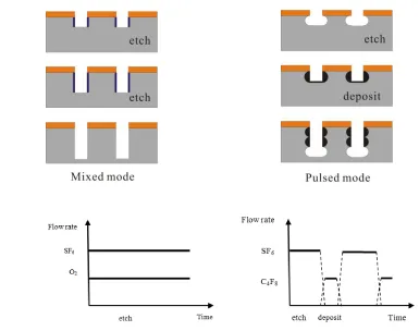
The difference between these two techniques lies in the way of adding inhibitor gases into plasma which will form the passivation layer during the etching process. In cryo-DRIE process, the inhibitor gas is added at the same time the etch gas enters ——thus also called mixed mode DRIE. In Bosch process, the inhibitor gas and etch gas are added in a sequence —— thus also called pulsed mode DRIE. The inhibitor gas in the former method is usually oxygen and the wafer is often cryogenically cooled to strengthen the inhibitor. In the latter method, the inhibitor is usually fluorocarbon gases which can perform strong polymer building [15]. See details in the figure 3.16.
In the pulsed mode, during the etch step a shallow trench is formed in the silicon substrate, with an isotropic profile characteristic of fluorine-rich glow discharges. During the passivation cycle, a protective fluorocarbon film is deposited on all surfaces. In the subsequent etch step, ion bombardment promotes the preferential removal of the film from all horizontal surfaces, allowing the profile to develop in a highly anisotropic fashion (Figure 3.16 top right). In a typical configuration SF6 is flowed during the etching cycle and C4F8 or CHF3 during the sidewall protection cycle. Compared to the mixed mode, the etch rate of pulsed mode is lower due to the paasivation layer deposition. In order for the directional etching to proceed, higher ionic impact should be applied to clean the bottom of the etching structures due to the thicker passivation layer. This also leads to a lower selectivity between mask and substrate. It is also shown one of the intrinsic features of pulsed mode DRIE in the figure——the scallops (figure 3.16 top right). This scalloping effect is caused by the etch/deposit cycle.
Figure 3.16 Top: Cross sectional view of trenches etched in both mix and pulsed mode. Bottom: flow rate versus
[image:28.612.93.478.187.491.2]23
3.2.3 High aspect ratio trench etching
High aspect ratio trench (HART) etching is one of the most important applications of DRIE. Profile control is extremely important during the HART etching. In the following parts, different effects in the profile control are discussed. These effects include RIE lag, bowing, bottling, and tilting [13,15,16].
There are two kinds of particles which are the main source for the etching in DRIE: ions and radicals. Ions are etching the passivating layer and controlling the profile by their direction. Radicals are necessary for etching the silicon. Normally, for an ion-inhibitor DRIE process, the high-density plasma has to wait for the incoming ion bombardment before it is able to remove silicon atoms. Therefore, the ion transportation from bulk plasma to the silicon surface is crucial to understand the etching process.
A molecule is hit by a fast moving electron and is ionized. This ion diffused with random thermal velocity to the plasma boundary (boundary between the bulk plasma and the sheath). The boundary distortion will influence the electric field and then influence the moving direction of ion which is entering the sheath region. When the ion passes the sheath region, it will collide with other particles. Therefore, due to the collision and thermal motion, the ion flux will disperse. This effect can be described by the ion angular or energy distribution function. After this the ion is entering the trench in which the ion deflection occurs because the electric field, from the conducting sample charging, will change the ion`s motion. The ion will end at the sidewall or the bottom of trench. Depending on the energy and collision angle it will reflect, etch, or just stay at the sidewall or trench bottom. A detailed discussion about different effects is as follows:
1. Tilting is caused by boundary distortion or local difference in radical density. Boundary distortion is found when sample geometry is greater than the thickness of sheath region. Lower the system pressure can increase the thickness of the sheath region and thus prevent this effect. Radical density difference will cause the radical flow from the high density area to the low density area, which will result in a non-vertical radical flux with respect to the silicon wafer surface. This can be minimized by making mask layout more uniform.
2. Bowing effect: This effect occurs in conducting samples. Ions in the trench will deflect due to the image force. Increasing the sidewall passivation or the energy of incoming ions before entering the trench would help to reduce this effect. This could be achieved in the cryogenic cooling condition or putting more passivation gas into the plasma.
24
the way of dc self-bias.
4. RIE lag: This effect can be explained in considering the amount of ions which exist during their travel in the trench. During the travel ions will deflect due to negative charged walls. Therefore, the ions will be captured by the walls. So the mount of ions reaching the bottom will be smaller. For smaller trenches, ion depletion is reached sooner than that of wider trenches because the flux/area ratio is smaller after certain etch depth. Another reason for this effect is the radical depletion. The radical flux is isotropic when entering the trench, but radical etching will cause decreasing of radicals to the bottom of trench. For smaller trenches, this is more pronounced after a certain depth.
3.2.4 Equipment
The DRIE system in the experiment is Adixen AMS 100SE DRIE system. This system can provide both the cryogenic and Bosch process with a temperature range between -180oC and +50oC. Feed gases include O2, SF6, CHF3, C4F8, Ar and will be converted into high density plasma by ICP on the top. To direct the ionic species toward the substrate, a CCP is connected to the system. Important qualification factors of such a DRIE system include ICP power, throttle position, SF6 flow, passivation gas flow, substrate holder distance, CCP power, temperature, and helium backside pressure. Etch rate and etch profile can be controlled by tuning the above parameters. In addition, the selectivity between the mask material and substrate is also influenced by these parameters. In the following, a general description [15,17]is given about the above parameters:
1. The ICP could influence the etch rate by creation of radical from feed gas in the plasma. At the same time, higher ICP power would create higher pressure in the chamber for the same amount of multi-atomic gas (SF6, CHF3, and C4F8). As the dark space width is direct proportional to the reciprocal of pressure, the lateral etching, caused by ion-gas collision during travel through dark space, could be influenced by ICP power.
2. Increasing etch gas flux can increase the etch speed due to more etch radicals in the plasma. However, for a certain ICP power the etch speed does not increase linearly with gas flux. It will increase till it reaches a maximum, then decreases.
3. Inhibitor gas is used to protect the sidewalls from etching. An increase in inhibitor gas flow decreases the etch-speed but results in better etch-profile anisotropy due to better side-wall passivation.
4. The throttle valve is related with the chamber pressure. The chamber pressure is increased by closing the exhaust throttle valve. An increased chamber pressure will have a bad effect on the etch-profile due to the increase in non-directional (lateral) etching. 5. CCP power is used to generate electric power, which accelerates the ions from the plasma
glow straight towards the substrate. The directional etch rate will increase due to more ion bombardment to remove the inhibitor layer. However, this results in low selectivity between the mask and substrate.
25 When it decreases, the etch rate increases due to high probability for the substrate to expose to the high density radical.
7. Wafer temperature has a big influence on the inhibitor`s passivation ability. The inhibitor layer formation is stronger in lower temperature, thus resulting in a better anisotropic etch-profile. However, in cryogenic condition, special attention has been paid to the crack of the mask material.
8. Wafer loading influences the etch rate because of depletion of radicals. Higher wafer loading consumes more radicals, which means lower the density of radicals, thus results in a decreasing of etch rate. Higher wafer loading also increases the wafer temperature.
In this experiment, it is designed to find the right DRIE recipe for wafer through etching (380um for (110) wafer) with a straight side wall and a good mask selectivity. The requested aspect ratio is 19:1. The tuning parameters in the recipe include the temperature, the CCP setting, and etching time, while other parameters are fixed. The etching mode is pulsed mode. Wafers are patterned with microsieve mask which has circular holes (Φ: 20-um) with a hexagonal pattern. Silicon loading is around 10% of a 100mm wafer (22.67% for the patterned area).
3.3 Surface roughness reduction
As discussed above, DRIE has become one of the most important processes in MEMS fabrication. The Bosch process is commonly used for vertical deep trench etching. Nevertheless, the Bosch process has its own drawbacks. One of them is the vertical sidewall roughness due to the periodical etching and deposition steps during process. A lot of efforts are made to reduce the surface roughness. Especially in the area of optical mirror techniques, because when the vertical is used as an optical mirror, the smooth sidewall is crucial to minimize the light scattering and maintain the collimated light beam. As reported in the literature [18-25], there are three main methods to reduce the sidewall roughness caused by Bosch process: 1. KOH wet anisotropic etching; 2. Hydrogen annealing; 3.thermal oxidation. In this report, the first two methods will be discussed.
26
3.3.1 KOH treatment
The scallops on the morphology of etched structures during DRIE can be removed by KOH wet anisotropic etching. Due to the high selectivity between {100}/{111} or {110}/{111} planes, etch will be very fast for {100}-and{110}-planes, while it is so slow for {111} planes as if it stops on this plane. As a result, etch will self-align with the restriction of {111} planes. Therefore, the sidewall smoothness of etched structures is mainly determined by the smoothness of the slowly etched {111} planes. A lot of studies have been done to investigate the surface morphology of different planes in etched structures in KOH solutions. Tellier [18] made a theoretical analysis about dependence of surface roughness on silicon crystal orientation. Later on, Sato [19] proposed an experimental proof for the relationship between surface roughness and crystal orientation. He performed his experiment by etching silicon spheres in the KOH solution. In his study the roughness of {111} planes is less than 100nm. He also showed that an increase in KOH concentration will improve the surface smoothness.
Vertical structures with smooth sidewalls can be fabricated on <110> silicon wafers with the mask align to the [111] crystal orientation. In the literature, a lot of studies on fabrication of
vertical optical mirror for MEMS devices [20-22] have been reported. In Yun`s study [20], the vertical mirror was made by using DRIE process and a successive KOH etching of a <110> SOI wafer. He also tried to improve the etching conditions for KOH solution. In his study, the optimal etching condition for KOH was found to be 45%wt concentration and 70oC temperature.
3.3.2 Hydrogen annealing
The hydrogen annealing has a great influence on the surface morphology of silicon substrate. Silicon atoms migration on the surface is enhanced by hydrogen at high temperature around 1000oC. Based on this feature, atomically smooth or regular arranged steps on <100> or <111> wafers can be achieved. This hydrogen-enhanced surface atom migration not only influences the surface morphology but also can change the global profile if the surface migration length is larger than or comparable to the structure dimensions. Previous experiment has reported to produce round corners and various voids by using hydrogen annealing in bulk silicon [23].
Figure 3.18 SEM pictures of the vertical sidewall measured in side view with respect to process time of KOH
27 The mechanism of atom migration in hydrogen annealing can be explained by surface diffusion theory. As the silicon is annealed in the hydrogen environment, the silicon surface will be terminated by H atoms. The global profile transformation is modeled as atom motion on an isotropic continuum (The transport of silicon atoms is actually determined by atomistic nature of crystals and is affected by the crystalline structure). The surface transport is dominated by surface diffusion and evaporation-condensation in the isotropic medium. However, for the annealing temperature less than 1100oC, surface diffusion has the main influence on the atom migration. Figure 1 shows a schematic of surface diffusion of silicon atoms. From figure 3.19, we can see that the atoms tend to leave the convex corners and accumulate at the concave corners.
In the literature, Mullins` theory of thermal grooving is used as the model to simulate the profile development.
𝑣 = 𝛾 ∗ 𝛺2∗ 𝑛 ∗ 𝐷 𝑘𝑇∗
𝜕2𝐾 𝜕𝑠2
Where the v is the profile developing speed, 𝜸 is the surface tension of the substrate, Ω is the molecular volume, n is the atom density, D is the diffusion coefficient, Tis the temperature, K is the surface curvature, and s is the arc length along the profile. The diffusion coefficient is determined by the temperature and pressure. Sato [23] explored this relationship with a trench evolution. He found the relationship as shown in figure 3.20. M. Lee [24] reported that the relationship between diffusion coefficient and temperature actually followed the Arrhenius equation. The pressure may only affect the activation energy of diffusion coefficient.
[image:33.612.131.522.229.437.2]28
Hydrogen-enhanced surface diffusion can effectively reduce the surface roughness. Therefore, it is possible to use this technique to reduce the scalloping effect in the Bosch process. M. Lee demonstrated sidewall scalloping was dramatically reduced by applying the hydrogen annealing [24].
Sacrificial thermal oxidation is another way to remove the surface roughness. The patterned structure is first oxidized then followed by an oxidation removal procedure. If necessary, these two steps can be repeated a few times to further reduce the surface roughness. However, it will not be used in this experiment because it will consume a lot of silicon and may also cause stress problems.
Figure 3.20 Time and pressure dependence of trench transformation. X and Y are defined as the long and short axis
of the trench
Figure 3.21 sidewall roughness caused by DRIE.(a) before and (b) after annealing[24]. The wafer was then annealed
29
Reference:
1. C. Kittel ―Introduction to solid state physics‖ 8th edition 2004. 2. H.V. Jansen ―MEMS based nanotechnology‖
3. Price, ―Semiconductor silicon‖ H.R. Huff and R.R. burgess, Editors, p.339, The electrochemical society softbound proceedings series Princeton NJ(1973)
4. Kendall, ―On etching very narrow grooves in silicon‖, Applied physics letters, Vol.26 No.4, 1975
5. E.D. Palik, H.F. Gray, and P.B. Klein,J. Electrochem. Soc. 130, 956 1983
6. E.D. Palik, V.M. Bermudez, and O. J. Glembocki, J. Electrochem. Soc. 132, 871 1985 7. E.D. Palik, V.M. Bermudez, and O. J. Glembocki, J. Electrochem. Soc. 132, 135 1985 8. N.F. Raley, y. Sugiyama, and T. van Duzer, J. Electrochem. Soc. 131, 161, 1984
9. H.Seidel, ―Anisotropic etching of crystalline silicon in Alkaline solutions‖, J. Electrochem. Soc. Vol.137, No.11 1990
10. M. Alavi, ‖ Fabrication of microchannels by laser machining and anisotropic etching of silicon‖, Sensors and Actuators A, 32 299 1992
11. Roland B. Gentemann, ―3D-fibre channels in silicon by electrical breakdown—New opportunities for optical fibre alignment and microfluidics‖, Int. J. Electron. Commun. (AEü) 61 (2007) 172 – 176
12. M.Sugawara, ―Plasma Etching: Fundamentals and Applications‖, Oxford university Press 1998
13. M.Elwenspoek, H.V. Jansen, ―Silicon Micromachining‖, Cambridge University Press 1998
14. Chapman B. N., ―Glow Discharge Processing‖ New York Wiley 1980
15. H.V. Jansen, ―Black silicon method X: a review on high speed and selective plasma etching of silicon with profile control: an in-depth comparison between Bosch and cryostat DRIE processes as a roadmap to next generation equipment‖, J. Micromech. Microeng. 19 (2009)
16. H.V. Jansen, ―A survey on the reactive ion etching of silicon in microtechnology‖, J. Micromech. Microeng. 6 (1996) 14–28
17. S. Unnikrishnan, ―MICROMACHINED DENSE PALLADIUM ELECTRODES FOR THIN-FILM SOLID ACID FUEL CELLS‖, PhD thesis, university of twente, 2009 18. Teller, ―Anisotropic etching of silicon crystal in KOH solutions‖, Journal of material
science 29,6354,1994
19. Kazuo Sato, ―Roughening of single-crystal silicon surface etched by KOH water solution‖, Sensors and Actuators 73 1999. 122–130
20. Sung-Sik Yun, ―Fabrication of vertical optical plane using DRIE and KOHcrystalline etching of (1 1 0) silicon wafer‖, Sensors and Actuators A 128 (2006) 387-394
21. Daesung Lee, ―Vertical Mirror Fabrication Combining KOH Etch and DRIE of (110) Silicon‖, JOURNAL OF MICROELECTROMECHANICAL SYSTEMS, VOL. 18, NO. 1, FEBRUARY 2009
22. R Agarwal, ―Fabrication of vertical mirrors using plasma etch and KOH: IPA polishing‖, J. Micromech. Microeng. 17 (2007) 26–35
30
hydrogen annealing,‖ Japan. J. Appl. Phys. Part 1-Regular Papers Short Notes Rev. Papers, vol. 39, pp. 5033–5038, 2000.
24. Ming-Chang M. Lee, ―Thermal Annealing in Hydrogen for 3-D Profile Transformation on Silicon-on-Insulator and Sidewall Roughness Reduction‖, Journal of microelectromechanical Systems, Vol. 15, No. 2, April 2006
31
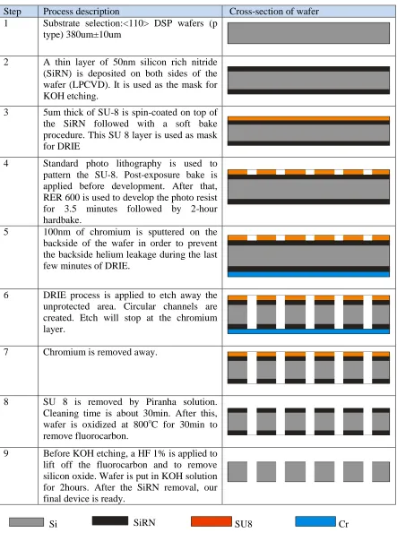
Chapter 4 Microsieve fabrication process
The fabrication of microsieve is done in the cleanroom of MESA+ institute of nanotechnology. Our aim is to make a rhombus shaped microsieve with smooth surface. The process starts with <110> wafers which are patterned with 20µm circular holes in a hexagonal pattern. After this, pulsed mode DRIE is applied to drill holes into the silicon. The aspect ratio after wafer-through etching for the 20µm holes is 19:1. After DRIE, there are periodical rough structures (so-called scallops) on the channel surface. This roughness is caused by the pulsed process and will be removed in a post-etch procedure using an anisotropic etch solution like KOH. During the KOH etch of the scalloped microsieve, most of the silicon planes are etching fast until the much more chemically stable {111} planes are reached. As a result, the originally circular channels become rhombus shaped channels with nano-scale smooth sidewalls.
4.1 Mask design
The mask is designed using the software CleWin3.0 from PhoeniX Software. The 5-inch mask has a design area of 10cm*10cm. Our pattern is located in a 8cm*8cm square centered at (0,0). Because the mask is designed for SU-8, a negative photoresist, the blue holes area is covered with chromium. For negative photoresist, photoresist from the non-exposed area will dissolve in the developer. The mask has a hexagonal pattern with hole`s diameter of 20um and the distance between the holes is 40um. The porosity of patterned area is 22.67% and the wafer loading is around 18.48%. The mask design is shown in figure 4.1.
4.2 Process Outline
The main process steps are shown in the following as well as a brief description of each step. Detailed discussion is made in the following paragraphs. For a detailed process, see the appendix C.
32
Table 4.1 process outline of microsieve fabrication
Step Process description Cross-section of wafer
1 Substrate selection:<110> DSP wafers (p type) 380um±10um
2 A thin layer of 50nm silicon rich nitride (SiRN) is deposited on both sides of the wafer (LPCVD). It is used as the mask for KOH etching.
3 5um thick of SU-8 is spin-coated on top of the SiRN followed with a soft bake procedure. This SU 8 layer is used as mask for DRIE
4 Standard photo lithography is used to pattern the SU-8. Post-exposure bake is applied before development. After that, RER 600 is used to develop the photo resist for 3.5 minutes followed by 2-hour hardbake.
5 100nm of chromium is sputtered on the backside of the wafer in order to prevent the backside helium leakage during the last few minutes of DRIE.
6 DRIE process is applied to etch away the unprotected area. Circular channels are created. Etch will stop at the chromium layer.
7 Chromium is removed away.
8 SU 8 is removed by Piranha solution. Cleaning time is about 30min. After this, wafer is oxidized at 800oC for 30min to remove fluorocarbon.
9 Before KOH etching, a HF 1% is applied to lift off the fluorocarbon and to remove silicon oxide. Wafer is put in KOH solution for 2hours. After the SiRN removal, our final device is ready.
SiRN
33 Equipment used in the experiment.
Name Usage
Tempress LPCVD G3 SiRN deposition
Plasmos Ellipsometer SiRN thickness measurement
SüssMicroTec Spinner Delta 20 SU 8 coating
Electronic Vision Group 620 Mask Aligner lithography
TCO Spray Developer SU 8 development
Nikon Microscope Optical microscopic inspection
Veeco Dektak 8 Surface profile measurement
Sputterke Cr spputering
Adixen 100SE DRIE process
Furnace B3 Dry oxidation
KOH wet bench KOH wet etching
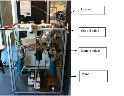
Another surface roughness reduction is performed by hydrogen annealing. The system used for hydrogen annealing is shown in figure 4.2
[image:39.612.98.516.349.672.2]
Figure 4.2 H2 annealing system
H2 inlet
Control valve
Sample holder
34
Chapter 5 Microsieve fabrication results and discussions
5.1 Lithography with SU 8 mask
SU-8 is a negative, epoxy type, near-UV photoresist that has been originally developed and patented by IBM. Due to its low optical absorption in UV range, this photoresist can form very thick film. The SU-8 resist contains a few percent of photoacid generator that will produce a strong acid when a photochemical transformation takes place upon absorption of a photon. This photoacid acts as a catalyst in the subsequent crosslinking reaction that takes place during post exposure bake (PEB), that is, crosslinking occurs only in regions that contain acid catalyst and mainly during PEB. This high-aspect-ratio resist, SU-8, leads itself well to MEMS applications. In this experiment there are two types of SU 8: SU 8-5 and SU 8-2005 from Microchem. We apply the same procedure for both of them. The procedure is as follows: (for detailed process flow, see the appendix C)
Table5.1 SU 8 process outline
Step Description Cross section
1 Substrate-(100) wafers 2 Standard cleaning
3 Dehydration bake @120oC for 10min 4 Spin coating with delta20 program 5
5 Softbake start @ 25oC; 1 min @ 50oC; 1 min @ 65oC 3 min @ 95oC; finish at 25oC.
6 Exposure using hard contact mode 10sec
7 Postbake start @ 25oC; 1 min @ 50oC; 1 min @ 65oC 2 min @ 80oC; finish at 25oC.
8 Development in RER 600 for 3:30min followed by RER 600 and IPA rinse
9 Optical microscope check cracks in SU 8 layer 10 Hardbake @120oC for 2 hours
11 Optical microscope check cracks in SU 8 layer 12 Veeco Dektak 8 check thickness of SU 8
SU 8-2005 is an upgraded version of SU 8-5 according to datasheet from the MicroChem Company. It is said that SU 8-2005 shows significantly improved wetting, faster drying and clean edge bead removal, which is also proved in our experiment. SU 8-5 is used as a substitute for SU 8-2005 due to SU 8-2005 supplement problem in the lab.
35 The first problem came across in the experiment is that part of SU 8 stuck on the mask when doing the exposure with the mask aligner. It happens almost on every wafer with SU 8-5 if the wafer is directly transferred from step 5 to step 6 in the above procedure (Table 5.1). However, after pre-exposure baking (softbake), if the wafers are kept in the room temperature for about 20 hours, the sticking problem occurs much less often. And if the wafers are kept for even longer time, i.e. more than 60 hours, the sticking problem will hardly happen. It turns out after a long time, the top surface layer of SU 8-5 transforms from liquid phase to solid phase and it is strong enough to withstand the force during the hard contact of exposure. For the wafers with SU 8-2005, sticking problem is not observed. To certain extent, this can prove that SU 8-2005 dries faster than the SU 8-5. Although the sticking problem ha
![Figure 2.1 flow regimes according to different Kn[2]](https://thumb-us.123doks.com/thumbv2/123dok_us/1205869.644126/10.612.96.516.268.378/figure-flow-regimes-according-different-kn.webp)
![Figure 3.3 Top: fundamental planes in silicon crystal. Bottom: side view of silicon crystal structure of three fundamental planes.[2]](https://thumb-us.123doks.com/thumbv2/123dok_us/1205869.644126/19.612.92.513.150.377/figure-fundamental-silicon-crystal-silicon-crystal-structure-fundamental.webp)
![Figure 3.19 Top: Schematic illustrating atom migration on surface. Bottom: cross section of a line and space pattern etched on bulk silicon; left:before annealing right:after annealing[24]](https://thumb-us.123doks.com/thumbv2/123dok_us/1205869.644126/33.612.131.522.229.437/figure-schematic-illustrating-migration-surface-silicon-annealing-annealing.webp)