Motorola reserves the right to make changes without further notice to any products herein. Motorola makes no warranty, representation or guarantee regarding the suitability of its products for any particular purpose, nor does Motorola assume any liability arising out of the application or use of any product or circuit, and specifically disclaims any and all liability, including without limitation consequential or incidental damages. “Typical” parameters which may be provided in Motorola data sheets and/or specifications can and do vary in different applications and actual performance may vary over time. All operating parameters, including “Typicals” must be validated for each customer application by customer’s technical experts. Motorola does not convey any license under its patent rights nor the rights of others. Motorola products are not designed, intended, or authorized for use as components in systems intended for surgical implant into the body, or other applications intended to support or sustain life, or for any other application in which the failure of the Motorola product could create a situation where personal injury or death may occur. Should Buyer purchase or use Motorola products for any such unintended or unauthorized application, Buyer shall indemnify and hold Motorola and its officers, employees, subsidiaries, affiliates, and distributors harmless against all claims, costs, damages, and expenses, and reasonable attorney fees arising out of, directly or indirectly, any claim of personal injury or death associated with such unintended or unauthorized use, even if such claim alleges that Motorola was negligent regarding the design or manufacture of the part. Motorola and are registered trademarks of Motorola, Inc. Motorola, Inc. is an Equal Opportunity/Affirmative Action Employer.
©Motorola, Inc., 2001
MSCAN
Block Guide
V02.14
Original Release Date: 19 MAY 1998 Revised: 18 SEP 2002
Revision History
Version Number
Revision Date
Effective
Date Author Description of Changes
0.0 5-19-98
Summary of changes: - First pass release.
- Started from Rev. 0.9 of the MSCAN12_2 spec. Changes include the following:
* MSCAN enable (CANE) bit added in CANCTL1 register. * RxCAN, TxCAN pins now available as GPIO on Port CANP0,1 respectively when MSCAN not enabled.
* Moved the Port CTL register after the PORT and DDR registers in order to place the PORT and DDR registers on an odd word boundary.
* Registers $__20 - $__3C are reserved and will read 0’s and writes will be unimplemented.
* Scan added per the HCS12 DFT document.
* Register and bit names updated per the HCS12 Module Requirements document.
* Converted spec to new TSCS Spec Template (Rev. 3.3) format, organization, and content. Spec was re-organized and some new sections added.
* Separated out customer information into Section 1 and moved all internal only information, i.e. conditional text, into Section 2 per the spec template.
* Cosmetic and clarification changes made.
* Changes to be less specific to the UDR12 world and more applicable to the CDR12 world.
* Eliminated “weasel” words, may and should.
* Rev. 0.9 spec tagging kept in tact with new functions tagged with temporary tags ({AT} - Additional Test, {T} - existing Test).
0.1 5-25-98 5-25-98 Summary of changes:
- Updates per individual spec reviews.
0.2 6-3-98
Summary of changes:
- Further clarification added in spec per Munich’s answers to various questions.
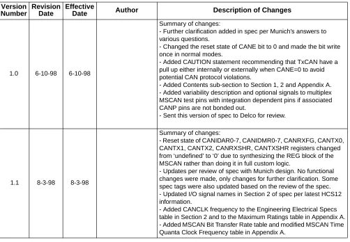
1.0 6-10-98 6-10-98
Summary of changes:
- Further clarification added in spec per Munich’s answers to various questions.
- Changed the reset state of CANE bit to 0 and made the bit write once in normal modes.
- Added CAUTION statement recommending that TxCAN have a pull up either internally or externally when CANE=0 to avoid potential CAN protocol violations.
- Added Contents sub-section to Section 1, 2 and Appendix A. - Added variability description and optional signals to multiplex MSCAN test pins with integration dependent pins if associated CANP pins are not bonded out.
- Sent this version of spec to Delco for review.
1.1 8-3-98 8-3-98
Summary of changes:
- Reset state of CANIDAR0-7, CANIDMR0-7, CANRXFG, CANTX0, CANTX1, CANTX2, CANRXSHR, CANTXSHR registers changed from ‘undefined’ to ‘0’ due to synthesizing the REG block of the MSCAN rather than doing it in full custom logic.
- Updates per review of spec with Munich design. No functional changes were made, only changes for further clarification. Some spec tags were also updated based on the review of the spec. - Updated I/O signal names in Section 2 of spec per latest HCS12 information.
[image:3.612.58.560.51.399.2]- Added CANCLK frequency to the Engineering Electrical Specs table in Section 2 and to the Maximum Ratings table in Appendix A. - Added MSCAN Bit Transfer Rate table and modified MSCAN Time Quanta Clock Frequency table in Appendix A.
Version Number
Revision Date
Effective
1.2 9-14-98 9-14-98
Summary of changes:
- Added RXACT flag in CANCTL0 register in bit 6 per the Project Change Request received from the Munich Design Center. This flag will provide an indication that the MSCAN is receiving a message.
- Added further clarification on low power options for Run, Wait, and Stop modes. Added description that the MSCAN clocks will shut down if MSCAN is disabled. Also added description regarding the disabling of input hysteresis in Wait & Stop modes.
- Clarified recovery from STOP or WAIT functionality. The MSCAN can wake the MCU up out of either STOP or WAIT via the wake-up interrupt if SLPAK=1.
- Added note regarding interrupt request clearing behavior--will be delayed one cycle once flag is cleared.
- Added further clarification on write conditions for CANIDAC and CANTEST registers.
- Added additional Warning for the receive & transmit error counter registers. May read an incorrect value if registers are read in any other mode other than sleep or soft reset and for MCUs with dual CPUs, may also cause a CPU fault condition to occur.
- Added additional Warning for reading the receive buffer registers. For MCUs with dual CPUs, may cause a CPU fault condition to occur if the receive buffers are read while the RXF flag is cleared. - Corrected the RDPCAN bit description. Reduced drive is not selectable for the TxCAN and RxCAN pins if the MSCAN is enabled.
- Added further clarification on CANPORT and CANDDR reads/writes of CANP1-0 when the MSCAN is enabled. - Enabled the pullups out of reset for the entire CAN port
(PUPCANE=1 out of reset). Removed cautions regarding the need to have an external pullup on TxCAN to avoid CAN protocol violations. Added further explanations regarding the protection mechanism against violating the CAN protocol (pullups enabled and CANE write once in normal modes).
- Removed scan information in DFT section in Section 2. Added that all clocks will be stopped when MCU is in scan mode. - Updated I/O signal list in Section 2.
- Updated module variability section in Section 2.
- Changed mscanclke signal in module variability section. Will not leave unconnected if MCU does not have an SCG module, but will use in the oscillator to enable the mscanclk.
- Added REGWRT bit to CANTEST register. Bit used to enable CPU write access to the test registers. Added bit and write descriptions. Modified RAMBO bit description.
- Updated test register read/write condition in Section 2. - Added Port CANP pin connections table in Section 2.
- Changed minimum bit transfer rate from dc to 10KBps in Appendix A, AC Electrical Characteristics section.
- Updated/added spec tags. Version
Number
Revision Date
Effective
1.3 10-05-98 10-05-98
Summary of Changes:
- Added bus activity flag for Volvo, RXFRM in CANCTL0 register in bit 7 per the Project Change Request received from the Munich Design Center. This flag will provide an indication that the MSCAN has received a valid message correctly.
- Added further clarification on how to program the CANIDMRx registers when receiving standard identifiers.
- Updated CANPORT and CANDDR read/write conditions per Architectural Definition review #3.
- Changed timer channel references from channel m to channel x to be consistent with signal name used in RTL.
- Spec tags updated per MSCAN requirements.
- Corrected write descriptions for CANCRCH/L, CANRXSHR, CANRXSHR registers in Section 2.
- Updated MSCAN clock enable module variations in Section 2. - Corrected spelling errors.
1.4 11-15-98 11-15-98
Summary of Changes:
- In register map, changed CANRXFG (foreground receive buffers) to indicate write is unimplemented.
- Changed REGWRT bit name to ECLOAD since bit is now used to load only the error counters with test data. Also changed the write conditions for this bit. It is no longer required for SFTRES to be set to write to ECLOAD.
- Changed the implementation for loading the error counters with a test value. Updated ECLOAD per the new implementation. Also added a description in CANRXERR and CANTXERR of how to load the error counters with a desired value in test mode.
- Updated max System and MSCAN clock frequency’s per decision to design all modules to 16MHz max.
- Changed vsc_smod_t4 to vsc_smod_t2 per smod timing change request.
- Added footnote for TWUP parameter in Appendix A. - Corrected Port CANP data out signal names in Table 2-4. - Update module I/O list in Section 2.
1.5 12-4-98 12-4-98
Summary of Changes:
- Added clarification for RXFRM and RXACT behaviour in loop back mode.
- Corrected format for CANRXERR and CANTXERR register write descriptions in Section 2.
1.6 1-10-99 1-10-99
Summary of Changes:
- Added CAUTION to CANDDR register description. Need to wait one cycle before reading the CANPORT register after writing to the CANDDR register when DDR changed to inputs.
1.7 3-9-99 3-9-99
Summary of Changes:
- Clarified Receive/Transmit buffer read/write capability.
- Updated Table 2-5 Engineering Electrical Specs min VDD from 2.7V to 3.0V.
Version Number
Revision Date
Effective
2.0 8-24-99 8-24-99
Summary of Changes:
- The required address space is reduced to 64 byte. The former MSCAN was a bit generous with the address map eating up 128byte per each module. By cutting it back it is possible to gain flexibility adding more CAN modules etc. In adition the transmit buffers are mapped to a transmit buffer window in address space. By having this window approach for the transmit buffer it is possible to seamless scale the number of transmit buffers up to 8 (although this is NOT planned yet). This requires also seperate registers for ABORT-Request and Abort-Acknowledge. In general this split eases the software and should not have an impact to those not using the abort feature. It is also possible to simplify and speed up the software addressing those buffers by using the TXWIN register. It is not neccessary to search for an empty buffer anymore. Also the destination address is logically the same which is very helpful when writing HC08 code (more than for HC12), since the HC08 has severe limitations with the one index register.
- The port interface is removed. The functionality will be provided by a separate external module. This will be generic to the HCS12 family , since for higher reuse efficiency want to sepearate the module functionality (e.g. CAN) from the chip dependant implementation (e.g. TXCAN signal tied to Port Module PCAN) - Full DFT compliant implementation (allows automatic scan chain insertion)
- 4 message buffers within the receiver FIFO ( instead of 2 in former designs). This was a strong request from the field and customers to improve the interupt latency, while keeping the programmers model.
- Enhanced clocking and reset strategy. The number of internal clocks was reduced to two clocks. The time quanta clock, the Rx-Bit clock and the pipelined clock pulses of the CAN clock domain are substituted by the internal CAN clock and a set of special clock enable signals which provide the same timing behavior for the MSCAN. All flip-flops in the design are asynchrounsly reset using the IPbus hard_rst_b signal.
- MSRS compliant IPbus interface substitutes the former HCS12 bus interface.
- The actual flags for warning and error are LEVEL sensitive, which is a bit tricky to handle in software. The actual change provides a interrupt-on-status-change for warning, and error level, as well as an indication of the actual status. The BUSOFF bit has not been changed.
-New Listen-Only Mode, which allows the MSCAN to monitor the CAN bus without generating acknowledges or error-frames by such a receive. In addition the error counters are not affected.
- Soft Reset Mode was changed to Initialization Mode. Due to a strict 2 clock -D-Flipflop strategy a minor change in the form known as SLPRQ was introduced. It is now a clear handshake
request-acknowledge. Impact is actually minor, since the handshke process is a matter of some clocks and is only of real importance if a very slow CAN clock in the range of 10kBits is used.
- Updated Table 2-2 Engineering Electrical Specs - Updated Table 2-1 MSCAN Module I/O Signals - Updated Register Map (check Figure 1-3) Version
Number
Revision Date
Effective
2.01 18-01-00 18-01-00
Summary of Changes:
- When Listen-Mode is active the TXEx flags in the CANTFLG register cannot be cleared and no CAN message is transmitted. - In special test mode the RxBuffers are read/writable from the IPbus side.
2.02 03-02-00 03-02-00
Summary of Changes: - Updated Spec.Tagging
- Reserved bits/bytes within Tx-/Rx-Buffer range are read as “x” instead of “0”
- Changed reset values for Tx-/Rx-Buffers
2.03 10-07-00 10-07-00
Summary of Changes:
- Updated Table 1-9 CPU vs. MSCAN Operating Modes - Corrected typo in INITAK handshake flag (1.7.1.2) - Updated wake-up note for WUPE flag (1.7.1.1)
2.04 21-08-00 21-08-00
Summary of Changes:
- Added information on the blocking mechanism for transmit buffers which are scheduled for transmission
(TXEx flag cleared) (see 1.7.1.7 & 1.7.1.11).
- Added information on the read value (’x’) for unused bits in the transmit/receive buffers (see 1.7.2).
2.05 08-11-00 08-11-00 Summary of Changes:
- Added 5th Rx Message Buffer to MSCAN.
2.06 20-11-00 20-11-00 - Reformated MSCAN spec form MMD-format to SRS2.0
V02.07 13 MAR 2001
13 MAR
2001 - Updated according to requirements of SRSv2 supplement.
V02.08 17 JUL 2001
17 JUL
2001 - 1st offical version by Technical Publishing
V02.09 10 JUL 2001
10 JUL 2001
- Updated according to requirements of SRSv3 - Corrected footnote 1 in INITRQ description.
V02.10 10 OCT 2001
10 OCT
2001 - Replaced all references w.r.t. new family name HCS12.
V02.11 22 OCT 2001
22 OCT 2001
- Corrected figure title and note of CANTIER.
- Corrected local enable register names in table 4-4 ’CRG Interrupt Vectors’.
- Updated block diagram.
- Corrected section ’Description of Interrupt Operation’.
V02.12 04 MAR 2002
04 MAR
2002 - Document format updates.
V02.13 22 JUL 2002
22 JUL 2002
- Corrected TBPR register offset.
- Corrected Table ’Message Buffer Organization’. - Corrected SLPRQ bit description.
- Corrected MSCAN Sleep Mode description. - Updated WUPE bit description.
- Updated Simplified State Transitions figure.
- Updated Recovery from STOP or WAIT description and CPU vs. MSCAN Modes table.
V02.14 18 SEP 2002
18 SEP 2002
- Added Initialization/Application information. - Replaced ’MCU’ with ’CPU’ in several places. - Cleaned up Mode descriptions.
- General cleanup. Version
Number
Revision Date
Effective
Table of Contents
Section 1 Introduction
1.1 Overview. . . 17
1.2 Features . . . 18
Section 2 External Signal Description
2.1 Overview. . . 192.2 Detailed Signal Description . . . 19
2.2.1 RXCAN — CAN Receiver Input Pin . . . 19
2.2.2 TXCAN — CAN Transmitter Output Pin. . . 19
2.3 CAN System . . . 19
Section 3 Memory Map/Register Definition
3.1 Overview. . . 213.2 Module Memory Map . . . 21
3.3 Register Descriptions . . . 22
3.3.1 Programmer’s Model of Control Registers . . . 23
3.3.2 Programmer’s Model of Message Storage. . . 44
Section 4 Functional Description
4.1 General. . . 504.2 Message Storage . . . 51
4.2.1 Message Transmit Background . . . 51
4.2.2 Transmit Structures . . . 52
4.2.3 Receive Structures. . . 53
4.3 Identifier Acceptance Filter . . . 54
4.3.1 Protocol Violation Protection . . . 58
4.3.2 Clock System . . . 58
4.4 Timer Link. . . 61
4.5 Modes of Operation . . . 61
4.5.1 Normal Modes . . . 61
4.5.2 Special Modes . . . 61
4.5.3 Emulation Modes . . . 61
4.5.5 Security Modes . . . 62
4.6 Low Power Options . . . 62
4.6.1 CPU Run Mode . . . 62
4.6.2 CPU Wait Mode . . . 63
4.6.3 CPU Stop Mode . . . 63
4.6.4 MSCAN Sleep Mode . . . 63
4.6.5 MSCAN Initialization Mode . . . 65
4.6.6 MSCAN Power Down Mode. . . 66
4.6.7 Programmable Wake-Up Function. . . 67
4.7 Reset Initialization . . . 67
4.8 General. . . 67
4.9 Description of Interrupt Operation . . . 68
4.9.1 Transmit Interrupt. . . 68
4.9.2 Receive Interrupt . . . 68
4.9.3 Wake-Up Interrupt . . . 68
4.9.4 Error Interrupt. . . 68
4.10 Interrupt Acknowledge . . . 68
4.11 Recovery from STOP or WAIT . . . 69
List of Figures
Figure 1-1 MSCAN Block Diagram . . . 17
Figure 2-1 The CAN System . . . 20
Figure 3-1 MSCAN Control 0 Register (CANCTL0) . . . 23
Figure 3-2 MSCAN Control 1 Register (CANCTL1) . . . 26
Figure 3-3 MSCAN Bus Timing Register 0 (CANBTR0) . . . 27
Figure 3-4 MSCAN Bus Timing Register 1 (CANBTR1) . . . 28
Figure 3-5 MSCAN Receiver Flag Register (CANRFLG) . . . 30
Figure 3-6 MSCAN Receiver Interrupt Enable Register (CANRIER) . . . 32
Figure 3-7 MSCAN Transmitter Flag Register (CANTFLG) . . . 34
Figure 3-8 MSCAN Transmitter Interrupt Enable Register (CANTIER) . . . 35
Figure 3-9 MSCAN Transmitter Message Abort Request (CANTARQ) . . . 35
Figure 3-10 MSCAN Transmitter Message Abort Control (CANTAAK) . . . 36
Figure 3-11 MSCAN Transmitter Flag Register (CANTBSEL) . . . 37
Figure 3-12 MSCAN Identifier Acceptance Control Register (CANIDAC). . . 38
Figure 3-13 Reserved Registers . . . 39
Figure 3-14 MSCAN Receive Error Counter Register (CANRXERR) . . . 40
Figure 3-15 MSCAN Transmit Error Counter Register (CANTXERR) . . . 40
Figure 3-16 MSCAN Identifier Acceptance Registers (1st Bank) . . . 41
Figure 3-17 MSCAN Identifier Acceptance Registers (2nd Bank) . . . 42
Figure 3-18 MSCAN Identifier Mask Registers (1st Bank) . . . 43
Figure 3-19 MSCAN Identifier Mask Registers (2nd Bank). . . 43
Figure 3-20 Receive / Transmit Message Buffer Extended Identifier . . . 45
Figure 3-21 Standard Identifier Mapping. . . 46
Figure 3-22 Transmit Buffer Priority Register (TBPR). . . 49
Figure 3-23 Time Stamp Register (TSRH - High Byte) . . . 49
Figure 3-24 Time Stamp Register (TSRL - Low Byte) . . . 49
Figure 4-1 User Model for Message Buffer Organization . . . 51
Figure 4-2 32-bit Maskable Identifier Acceptance Filter . . . 56
Figure 4-3 16-bit Maskable Identifier Acceptance Filters . . . 56
Figure 4-4 8-bit Maskable Identifier Acceptance Filters . . . 57
Figure 4-5 MSCAN Clocking Scheme. . . 58
Figure 4-6 Segments within the Bit Time . . . 60
List of Tables
Table 3-1 MSCAN Register Organization . . . 21
Table 3-2 Module Memory Map . . . 21
Table 3-3 Synchronization Jump Width . . . 28
Table 3-4 Baud Rate Prescaler . . . 28
Table 3-5 Time Segment 2 Values. . . 29
Table 3-6 Time Segment 1 Values. . . 30
Table 3-7 Identifier Acceptance Mode Settings . . . 38
Table 3-8 Identifier Acceptance Hit Indication . . . 39
Table 3-9 Message Buffer Organization . . . 45
Table 3-10 Data length codes . . . 48
Table 4-1 Time Segment Syntax . . . 60
Table 4-2 CAN Standard Compliant Bit Time Segment Settings . . . 61
Table 4-3 CPU vs. MSCAN Operating Modes . . . 62
Preface
Terminology
Acronyms and Abbreviations
ACK Acknowledge
CAN Controller Area Network
CRC Cyclic Redundancy Code
EOF End of Frame
FIFO First-In-First-Out Memory
IFS Inter-Frame Sequence
MSCAN Motorola Scalable CAN Module
Section 1 Introduction
1.1 Overview
The Motorola Scalable Controller Area Network (MSCAN) definition is based on the MSCAN12 definition which is the specific implementation of the Motorola Scalable CAN concept targeted for the Motorola MC68HC12 Microcontroller Family.
The module is a communication controller implementing the CAN 2.0 A/B protocol as defined in the BOSCH specification dated September 1991. For users to fully understand the MSCAN specification, it is recommended that the Bosch specification be read first to familiarize the reader with the terms and concepts contained within this document.
The CAN protocol was primarily, but not only, designed to be used as a vehicle serial data bus, meeting the specific requirements of this field: real-time processing, reliable operation in the EMI environment of a vehicle, cost-effectiveness and required bandwidth.
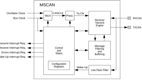
[image:17.612.71.548.348.623.2]MSCAN utilizes an advanced buffer arrangement resulting in a predictable real-time behavior and simplifies the application software.
Figure 1-1 MSCAN Block Diagram
RXCAN
TXCAN Receive/
Transmit Engine
Message Filtering
and Buffering Control
and Status Wake-Up Interrupt Req.
Errors Interrupt Req. Receive Interrupt Req. Transmit Interrupt Req.
CANCLK
Bus Clock
Configuration Oscillator Clock
MUX Presc. Tq Clk
MSCAN
Low Pass Filter Wake-Up
1.2 Features
The basic features of the MSCAN are as follows:
• Implementation of the CAN protocol - Version 2.0A/B
– Standard and extended data frames
– 0 - 8 bytes data length
– Programmable bit rate up to 1 Mbps1
– Support for remote frames
– 5 receive buffers with FIFO storage scheme
• 3 transmit buffers with internal prioritization using a “local priority” concept
• Flexible maskable identifier filter supports two full size extended identifier filters (two 32-bit) or four 16-bit filters or eight 8-bit filters
• Programmable wake-up functionality with integrated low-pass filter
• Programmable loop back mode supports self-test operation
• Programmable listen-only mode for monitoring of CAN bus
• Separate signalling and interrupt capabilities for all CAN receiver and transmitter error states (Warning, Error Passive, Bus-Off)
• Programmable MSCAN clock source either Bus Clock or Oscillator Clock
• Internal timer for time-stamping of received and transmitted messages
• Three low power modes: Sleep, Power Down and MSCAN Enable
• Global initialization of configuration registers
NOTES:
Section 2 External Signal Description
2.1 Overview
This section lists and describes the signals that connect off chip.
2.2 Detailed Signal Description
The MSCAN uses two external pins.
2.2.1 RXCAN — CAN Receiver Input Pin
RXCAN is the MSCAN receiver input pin.
2.2.2 TXCAN — CAN Transmitter Output Pin
TXCAN is the MSCAN transmitter output pin. The TXCAN output pin represents the logic level on the CAN bus:
0 = Dominant state 1 = Recessive state
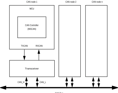
2.3 CAN System
Figure 2-1 The CAN System
CAN Bus CAN Controller
(MSCAN)
Transceiver
CAN node 1 CAN node 2 CAN node n
CAN_L CAN_H
MCU
Section 3 Memory Map/Register Definition
3.1 Overview
This section provides a detailed description of all registers accessible in the MSCAN.
3.2 Module Memory Map
Table 3-1 andTable 3-2 give an overview on all registers and their individual bits in the MSCAN memory map. The register address results from the addition of base address and address offset. The base
address is determined at the MCU level. The address offset is defined at the module level.
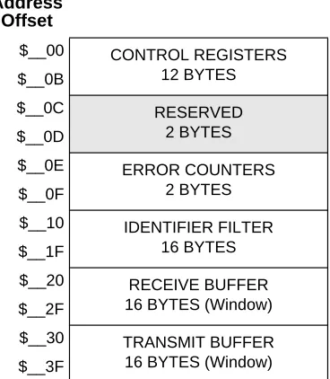
[image:21.612.219.403.312.523.2]The MSCAN occupies 64 bytes in the memory space. The base address of the MSCAN module is determined at the MCU level when the MCU is defined. The register decode map is fixed and begins at the first address of the module address offset.
Table 3-1 MSCAN Register Organization
Table 3-1 shows the individual registers associated with the MSCAN and their relative offset from the base address. The detailed register descriptions follow in the order they appear in the register map (see Table 3-2).
Table 3-2 Module Memory Map
Address Offset
$__00 CONTROL REGISTERS
12 BYTES $__0B
$__0C RESERVED
2 BYTES $__0D
$__0E ERROR COUNTERS
2 BYTES $__0F
$__10 IDENTIFIER FILTER
16 BYTES $__1F
$__20 RECEIVE BUFFER
16 BYTES (Window) $__2F
$__30 TRANSMIT BUFFER
16 BYTES (Window) $__3F
Address Use Access
$__00 MSCAN Control Register 0 (CANCTL0) R/W1
$__01 MSCAN Control Register 1 (CANCTL1) R/W1
$__02 MSCAN Bus Timing Register 0 (CANBTR0) R/W
3.3 Register Descriptions
This section describes in detail all the registers and register bits in the MSCAN module. Each description includes a standard register diagram with an associated figure number. Details of register bit and field function follow the register diagrams, in bit order. All bits of all registers in this module are completely synchronous to internal clocks during a register read.
$__04 MSCAN Receiver Flag Register (CANRFLG) R/W1
$__05 MSCAN Receiver Interrupt Enable Register (CANRIER) R/W
$__06 MSCAN Transmitter Flag Register (CANTFLG) R/W1
$__07 MSCAN Transmitter Interrupt Enable Register (CANTIER) R/W1
$__08 MSCAN Transmitter Message Abort Control (CANTARQ) R/W1
$__09 MSCAN Transmitter Message Abort Control (CANTAAK) R
$__0A MSCAN Transmit Buffer Selection (CANTBSEL) R/W1
$__0B MSCAN Identifier Acceptance Control Register (CANIDAC) R/W1
$__0C
-$__0D RESERVED
$__0E MSCAN Receive Error Counter Register (CANRXERR) R
$__0F MSCAN Transmit Error Counter Register (CANTXERR) R
$__10 MSCAN Identifier Acceptance Register 0 (CANIDAR0) R/W
$__11 MSCAN Identifier Acceptance Register 1 (CANIDAR1) R/W
$__12 MSCAN Identifier Acceptance Register 2 (CANIDAR2) R/W
$__13 MSCAN Identifier Acceptance Register 3 (CANIDAR3) R/W
$__14 MSCAN Identifier Mask Register 0 (CANIDMR0) R/W
$__15 MSCAN Identifier Mask Register 1 (CANIDMR1) R/W
$__16 MSCAN Identifier Mask Register 2 (CANIDMR2) R/W
$__17 MSCAN Identifier Mask Register 3 (CANIDMR3) R/W
$__18 MSCAN Identifier Acceptance Register 4 (CANIDAR4) R/W
$__19 MSCAN Identifier Acceptance Register 5 (CANIDAR5) R/W
$__1A MSCAN Identifier Acceptance Register 6 (CANIDAR6) R/W
$__1B MSCAN Identifier Acceptance Register 7 (CANIDAR7) R/W
$__1C MSCAN Identifier Mask Register 4 (CANIDMR4) R/W
$__1D MSCAN Identifier Mask Register 5 (CANIDMR5) R/W
$__1E MSCAN Identifier 6 Mask Register 6 (CANIDMR6) R/W
$__1F MSCAN Identifier Mask Register 7 (CANIDMR7) R/W
$__20
-$__2F Foreground Receive Buffer (CANRXFG) R2
$__30
-$__3F Foreground Transmit Buffer (CANTXFG) R2/W
NOTES:
1. Refer to detailed register description for write access restrictions on per bit basis. 2. Reserved bits and unused bits within the TX- and RX-Buffers (CANTXFG,
3.3.1 Programmer’s Model of Control Registers
The programmer’s model is laid out for maximum simplicity and efficiency.Table 3-2 provides an overview of the control registers for the MSCAN.
3.3.1.1 MSCAN Control 0 Register (CANCTL0)
The CANCTL0 register provides for various control of the MSCAN module as described below.
NOTE: The CANCTL0 register, except the WUPE, INITRQ and SLPRQ bits, is held in the reset state when the Initialization Mode is active (INITRQ=1 and INITAK=1). This register is writable again as soon as the Initialization Mode is left (INITRQ=0 and INITAK=0).
Read: Anytime
Write: Anytime when out of Initialization Mode; exceptions are read-only bits RXACT and SYNCH, bit RXFRM which is set by the module only and bit INITRQ which is also writable in Initialization Mode.
RXFRM — Received Frame Flag
This bit is read and clear only. It is set when a receiver has received a valid message correctly, independently of the filter configuration. Once set, it remains set until cleared by software or reset. Clearing is done by writing a ‘1’ to the bit. A write ‘0’ is ignored. This bit is not valid in loop back mode.
1 = A valid message was received since last clearing of this flag 0 = No valid message was received since last clearing this flag.
NOTE: The MSCAN must be in Normal Mode for this bit to become set.
RXACT — Receiver Active Status
This read-only flag indicates the MSCAN is receiving a message. The flag is controlled by the receiver front end. This bit is not valid in loop back mode.
1 = MSCAN is receiving a message (including when arbitration is lost)1 0 = MSCAN is transmitting or idle1.
Address Offset: $__00
Bit 7 6 5 4 3 2 1 Bit 0
Read:
RXFRM
RXACT
CSWAI
SYNCH
TIME WUPE SLPRQ INITRQ
Write:
Reset: 0 0 0 0 0 0 0 1
= Unimplemented
CSWAI — CAN Stops in Wait Mode
Enabling this bit allows for lower power consumption in Wait Mode by disabling all the clocks at the bus interface to the MSCAN module.
1 = The module ceases to be clocked during Wait Mode. 0 = The module is not affected during Wait Mode.
NOTE: In order to protect from accidentally violating the CAN protocol the TXCAN pin is immediately forced to a recessive state when the CPU enters Wait (CSWAI=1) or Stop Mode (see4.6.2 CPU Wait Mode and4.6.3 CPU Stop Mode)
SYNCH — Synchronized Status
This read-only flag indicates whether the MSCAN is synchronized to the CAN bus and, as such, can participate in the communication process. It is set and cleared by the MSCAN.
1 = MSCAN is synchronized to the CAN bus. 0 = MSCAN is not synchronized to the CAN bus.
TIME - Timer Enable
This bit activates an internal 16-bit wide free running timer which is clocked by the bit clock. If the timer is enabled, a 16-bit time stamp will be assigned to each transmitted/received message within the active TX/RX buffer. As soon as a message is acknowledged on the CAN bus, the time stamp will be written to the highest bytes ($_E, $_F) in the appropriate buffer3.3.2 Programmer’s Model of Message Storage. The internal timer is reset (all bits set to “0”) when Initialization Mode is active.
1 = Enable internal MSCAN timer. 0 = Disable internal MSCAN timer.
WUPE — Wake-Up Enable
This configuration bit allows the MSCAN to restart from Sleep Mode when traffic on CAN is detected (see4.6.4 MSCAN Sleep Mode).
1 = Wake-Up enabled– The MSCAN is able to restart.
0 = Wake-Up disabled– The MSCAN ignores traffic on CAN.
NOTE: The CPU has to make sure that the WUPE register and the WUPIE Wake-Up interrupt enable register3.3.1.6 MSCAN Receiver Interrupt Enable
Register (CANRIER)is enabled, if the recovery mechanism from STOP or WAIT is required.
SLPRQ — Sleep Mode Request
This bit requests the MSCAN to enter Sleep Mode, which is an internal power saving mode (see4.6.4 MSCAN Sleep Mode). The Sleep Mode request is serviced when the CAN bus is idle, i.e. the module is not receiving a message and all transmit buffers are empty. The module indicates entry to Sleep Mode by setting SLPAK=1 (3.3.1.2 MSCAN Control 1 Register (CANCTL1)). Sleep Mode will be active until SLPRQ is cleared by the CPU or, depending on the setting of WUPE bit, the MSCAN detects bus activity on CAN and clears the SLPRQ itself.
NOTES:
1 = Sleep Mode Request – The MSCAN enters Sleep Mode when CAN bus idle. 0 = Running – The MSCAN functions normally.
NOTE: The CPU cannot clear the SLPRQ bit before the MSCAN has entered Sleep Mode (SLPRQ=1 and SLPAK=1)
INITRQ — Initialization Mode Request
When this bit is set by the CPU, the MSCAN skips to Initialization Mode (see4.6.5 MSCAN Initialization Mode). Any ongoing transmission or reception is aborted and synchronization to the bus is lost. The module indicates entry to Initialization Mode by setting INITAK=1 (3.3.1.2 MSCAN Control 1 Register (CANCTL1)).
The following registers enter their hard reset state and restore their default values: CANCTL01, CANRFLG2, CANRIER3, CANTFLG, CANTIER, CANTARQ, CANTAAK, CANTBSEL. The registers CANCTL1, CANBTR0, CANBTR1, CANIDAC, CANIDAR0-7, CANIDMR0-7 can only be written by the CPU when the MSCAN is in Initialization Mode (INITRQ=1 and INITAK=1). The values of the error counters are not affected by Initialization Mode.
When this bit is cleared by the CPU, the MSCAN restarts and then tries to synchronize to the CAN bus. If the MSCAN is not in Bus-Off state, it synchronizes after 11 consecutive recessive bits on the bus; if the MSCAN is in Bus-Off state it continues to wait for 128 occurrences of 11 consecutive recessive bits.
Writing to other bits in CANCTL0, CANRFLG, CANRIER, CANTFLG or CANTIER must only be done after Initialization Mode is left, which is INITRQ=0 and INITAK=0.
1 = MSCAN in Initialization Mode. 0 = Normal operation.
NOTE: The CPU cannot clear the INITRQ bit before the MSCAN has entered Initialization Mode (INITRQ=1 and INITAK=1)
NOTE: In order to protect from accidentally violating the CAN protocol the TXCAN pin is immediately forced to a recessive state when the Initialization Mode is requested by the CPU. Thus the recommended procedure is to bring the MSCAN into Sleep Mode (SLPRQ=1 and SLPAK=1) before.
3.3.1.2 MSCAN Control 1 Register (CANCTL1)
The CANCTL1 register provides for various control and handshake status information of the MSCAN module as described below.
NOTES:
1. Except the WUPE, INITRQ and SLPRQ bits
2. The TSTAT1, TSTAT0 bits are not affected by Initialization Mode 3. The RSTAT1, RSTAT0 bits are not affected by Initialization Mode
Read: Anytime
Write: Anytime when INITRQ=1 and INITAK=1, except CANE which is write once in normal and anytime in special system operation modes when the MSCAN is in Initialization Mode (INITRQ=1 and INITAK=1).
CANE — MSCAN Enable
1 = The MSCAN module is enabled. 0 = The MSCAN module is disabled.
CLKSRC — MSCAN Clock Source
This bit defines the clock source for the MSCAN module (only for systems with a clock generation module;4.3.2 Clock System andFigure 4-5).
1 = The MSCAN clock source is the Bus Clock. 0 = The MSCAN clock source is the Oscillator Clock.
LOOPB — Loop Back Self Test Mode
When this bit is set, the MSCAN performs an internal loop back which can be used for self test operation. The bit stream output of the transmitter is fed back to the receiver internally. The RXCAN input pin is ignored and the TXCAN output goes to the recessive state (logic ‘1’). The MSCAN behaves as it does normally when transmitting and treats its own transmitted message as a message received from a remote node. In this state, the MSCAN ignores the bit sent during the ACK slot in the CAN frame Acknowledge field to ensure proper reception of its own message. Both transmit and receive interrupts are generated.
1 = Loop Back Self Test enabled 0 = Loop Back Self Test disabled
LISTEN — Listen Only Mode
This bit configures the MSCAN as a bus monitor. When the bit is set, all valid CAN messages with matching ID are received, but no acknowledgement or error frames are sent out4.5.4 Listen-Only Mode. In addition the error counters are frozen.
Listen Only Mode supports applications which require “hot plugging” or throughput analysis. The MSCAN is unable to transmit any messages, when Listen Only Mode is active.
1 = Listen Only Mode activated 0 = Normal operation
WUPM — Wake-Up Mode
Bit 7 6 5 4 3 2 1 Bit 0
Read:
CANE CLKSRC LOOPB LISTEN
0
WUPM
SLPAK INITAK
Write:
Reset: 0 0 0 1 0 0 0 1
= Unimplemented
This bit defines whether the integrated low-pass filter is applied to protect the MSCAN from spurious wake-up4.6.4 MSCAN Sleep Mode.
1 = MSCAN wakes-up the CPU only in case of a dominant pulse on the bus which has a length of Twupand WUPE=1 in CANCTL0 (see3.3.1.1 MSCAN Control 0 Register (CANCTL0)). 0 = MSCAN wakes-up the CPU after any recessive to dominant edge on the CAN bus and WUPE=1
in CANCTL0.
SLPAK — Sleep Mode Acknowledge
This flag indicates whether the MSCAN module has entered Sleep Mode4.6.4 MSCAN Sleep Mode. It is used as a handshake flag for the SLPRQ Sleep Mode request. Sleep Mode is active when SLPRQ=1 and SLPAK=1. Depending on the setting of the WUPE bit the MSCAN will clear the flag if it detects bus activity on CAN while in Sleep Mode.
1 = Sleep Mode Active – The MSCAN has entered Sleep Mode. 0 = Running – The MSCAN operates normally.
INITAK — Initialization Mode Acknowledge
This flag indicates whether the MSCAN module is in Initialization Mode4.6.5 MSCAN
Initialization Mode. It is used as a handshake flag for the INITRQ Initialization Mode request. Initialization Mode is active when INITRQ=1 and INITAK=1.
The registers CANCTL1, CANBTR0, CANBTR1, CANIDAC, CANIDAR0-7, CANIDMR0-7 can only be written by the CPU when the MSCAN is in Initialization Mode.
1 = Initialization Mode Active – The MSCAN has entered Initialization Mode. 0 = Running – The MSCAN operates normally.
3.3.1.3 MSCAN Bus Timing Register 0 (CANBTR0)
The CANBTR0 register provides for various bus timing control of the MSCAN module as described below.
Read: Anytime
Write: Anytime in Initialization Mode (INITRQ=1 and INITAK=1)
SJW1, SJW0 — Synchronization Jump Width
Address Offset: $__02
Bit 7 6 5 4 3 2 1 Bit 0
Read:
SJW1 SJW0 BRP5 BRP4 BRP3 BRP2 BRP1 BRP0
Write:
Reset: 0 0 0 0 0 0 0 0
The synchronization jump width defines the maximum number of time quanta (Tq) clock cycles a bit can be shortened or lengthened to achieve resynchronization to data transitions on the bus (seeTable 3-3).
BRP[5-0] — Baud Rate Prescaler
These bits determine the time quanta (Tq) clock which is used to build up the individual bit timing, as shown inTable 3-4.
3.3.1.4 MSCAN Bus Timing Register 1 (CANBTR1)
The CANBTR1 register provides for various bus timing control of the MSCAN module as described below.
Table 3-3 Synchronization Jump Width
SJW1 SJW0 Synchronization jump width
0 0 1 Tq clock cycle
0 1 2 Tq clock cycles
1 0 3 Tq clock cycles
1 1 4 Tq clock cycles
Table 3-4 Baud Rate Prescaler
BRP5 BRP4 BRP3 BRP2 BRP1 BRP0 Prescalervalue (P)
0 0 0 0 0 0 1
0 0 0 0 0 1 2
0 0 0 0 1 0 3
0 0 0 0 1 1 4
: : : : : : :
1 1 1 1 1 0 63
1 1 1 1 1 1 64
Address Offset: $__03
Bit 7 6 5 4 3 2 1 Bit 0
Read:
SAMP TSEG22 TSEG21 TSEG20 TSEG13 TSEG12 TSEG11 TSEG10 Write:
Read: Anytime
Write: Anytime in Initialization Mode (INITRQ=1 and INITAK=1)
SAMP — Sampling
This bit determines the number of samples of the serial bus to be taken per bit time. If set, three samples per bit are taken; the regular one (sample point) and two preceding samples using a majority rule. For higher bit rates, it is recommended that SAMP be cleared which means that only one sample is taken per bit.
1 = Three samples per bit1. 0 = One sample per bit.
TSEG22 – TSEG20 — Time Segment 2
Time segments within the bit time fix the number of clock cycles per bit time and the location of the sample point (seeFigure 4-6 Segments within the Bit Time).
Time segment 2 (TSEG2) values are programmable as shown inTable 3-5.
TSEG13 – TSEG10 — Time Segment 1
Time segments within the bit time fix the number of clock cycles per bit time and the location of the sample point (seeFigure 4-6 Segments within the Bit Time).
Time segment 1 (TSEG1) values are programmable as shown inTable 3-6.
Reset: 0 0 0 0 0 0 0 0
NOTES:
1. In this case, PHASE_SEG1 must be at least 2 Time Quanta.
Table 3-5 Time Segment 2 Values
TSEG22 TSEG21 TSEG20 Time segment 2
0 0 0 1 Tq clock cycle1
NOTES:
1. This setting is not valid. Please refer to Table 4-2 CAN Standard Compliant Bit
Time Segment Settings for valid settings.
0 0 1 2 Tq clock cycles
. . . .
1 1 0 7 Tq clock cycles
1 1 1 8 Tq clock cycles
The bit time is determined by the oscillator frequency, the baud rate prescaler, and the number of time quanta (Tq) clock cycles per bit (as shown inTable 3-5 andTable 3-6 above).
3.3.1.5 MSCAN Receiver Flag Register (CANRFLG)
A flag can only be cleared when the condition which caused the setting is no longer valid and can only be cleared by software (writing a ‘1’ to the corresponding bit position). Every flag has an associated interrupt enable bit in the CANRIER register.
Table 3-6 Time Segment 1 Values
TSEG13 TSEG12 TSEG11 TSEG10 Time segment 1
0 0 0 0 1 Tq clock cycle1
NOTES:
1. This setting is not valid. Please refer to Table 4-2 CAN Standard Compliant Bit Time
Segment Settings for valid settings.
0 0 0 1 2 Tq clock cycles1
0 0 1 0 3 Tq clock cycles1
0 0 1 1 4 Tq clock cycles
. . . . .
1 1 1 0 15 Tq clock cycles
1 1 1 1 16 Tq clock cycles
Address Offset: $__04
Bit 7 6 5 4 3 2 1 Bit 0
Read:
WUPIF CSCIF
RSTAT1 RSTAT0 TSTAT1 TSTAT0
OVRIF RXF
Write:
Reset: 0 0 0 0 0 0 0 0
Figure 3-5 MSCAN Receiver Flag Register(CANRFLG)
Bit Time (Prescaler value) fCANCLK
NOTE: The CANRFLG register is held in the reset state1 when the Initialization Mode is active (INITRQ=1 and INITAK=1). This register is writable again as soon as the Initialization Mode is left (INITRQ=0 and INITAK=0).
Read: Anytime
Write: Anytime when out of Initialization Mode, except RSTAT[1:0] and TSTAT[1:0] flags which are read-only; write of ‘1’ clears flag; write of ‘0’ ignored
WUPIF — Wake-Up Interrupt Flag
If the MSCAN detects bus activity while in Sleep Mode4.6.4 MSCAN Sleep Mode and the WUPE=1 in CANTCTL0 (see3.3.1.1 MSCAN Control 0 Register (CANCTL0)), it will set the WUPIF flag. If not masked, a Wake-Up interrupt is pending while this flag is set.
1 = MSCAN detected activity on the bus and requested wake-up. 0 = No wake-up activity observed while in Sleep Mode.
CSCIF — CAN Status Change Interrupt Flag
This flag is set when the MSCAN changes its current bus status due to the actual value of the Transmit Error Counter (TEC) and the Receive Error Counter (REC). An additional 4-bit (RSTAT[1:0], TSTAT[1:0]) status register, which is split into separate sections for TEC/REC, informs the system on the actual bus status3.3.1.6 MSCAN Receiver Interrupt Enable Register (CANRIER). If not masked, an Error interrupt is pending while this flag is set. CSCIF provides a blocking interrupt. That guarantees that the Receiver / Transmitter status bits (RSTAT/TSTAT) are only updated when no CAN Status Change interrupt is pending. If the TECs/RECs change their current value after the CSCIF is asserted and therefore would cause an additional state change in the RSTAT/TSTAT bits, these bits keep their old state bits until the current CSCIF interrupt is cleared again.
1 = MSCAN changed current bus status.
0 = No change in bus status occurred since last interrupt.
RSTAT1, RSTAT0 — Receiver Status Bits
The values of the error counters control the actual bus status of the MSCAN. As soon as the Status Change Interrupt Flag (CSCIF) is set these bits indicate the appropriate receiver related bus status of the MSCAN. The coding for the bits RSTAT1, RSTAT0 is:
00 = RxOK: 0≤ Receive Error Counter≤ 96 01 = RxWRN: 96 < Receive Error Counter≤ 127 10 = RxERR: 127 < Receive Error Counter
11 = Bus-Off2: Transmit Error Counter > 255
TSTAT1, TSTAT0 — Transmitter Status Bits
The values of the Error Counters control the actual bus status of the MSCAN. As soon as the Status Change Interrupt Flag (CSCIF) is set these bits indicate the appropriate transmitter related bus status of the MSCAN. The coding for the bits TSTAT1, TSTAT0 is:
NOTES:
1. The RSTAT[1:0], TSTAT[1:0] bits are not affected by Initialization Mode
00 = TxOK: 0≤Transmit Error Counter≤ 96 01 = TxWRN: 96 < Transmit Error Counter≤ 127 10 = TxERR: 127 < Transmit Error Counter≤ 255 11 = Bus-Off: Transmit Error Counter > 255
OVRIF — Overrun Interrupt Flag
This flag is set when a data overrun condition occurs. If not masked, an Error interrupt is pending while this flag is set.
1 = A data overrun detected. 0 = No data overrun condition.
RXF — Receive Buffer Full Flag
The RXF flag is set by the MSCAN when a new message is shifted in the receiver FIFO. This flag indicates whether the shifted buffer is loaded with a correctly received message (matching identifier, matching Cyclic Redundancy Code (CRC) and no other errors detected). After the CPU has read that message from the RxFG buffer in the receiver FIFO, the RXF flag must be cleared to release the buffer. A set RXF flag prohibits the shifting of the next FIFO entry into the foreground buffer (RxFG). If not masked, a Receive interrupt is pending while this flag is set.
1 = The receiver FIFO is not empty. A new message is available in the RxFG. 0 = No new message available within the RxFG.
NOTE: To ensure data integrity, do not read the receive buffer registers while the RXF flag is cleared.
For MCUs with dual CPUs, reading the receive buffer registers while the RXF flag is cleared may result in a CPU fault condition.
3.3.1.6 MSCAN Receiver Interrupt Enable Register (CANRIER)
This register contains the interrupt enable bits for the interrupt flags described above.
NOTE: The CANRIER register is held in the reset state1 when the Initialization Mode is active (INITRQ=1 and INITAK=1). This register is writable again as soon as the Initialization Mode is left (INITRQ=0 and INITAK=0).
Address Offset: $__05
Bit 7 6 5 4 3 2 1 Bit 0
Read:
WUPIE CSCIE RSTATE1 RSTATE0 TSTATE1 TSTATE0 OVRIE RXFIE Write:
Reset: 0 0 0 0 0 0 0 0
Figure 3-6 MSCAN Receiver Interrupt Enable Register(CANRIER)
NOTES:
Read: Anytime
Write: Anytime when out of Initialization Mode
WUPIE — Wake-Up Interrupt Enable
1 = A wake-up event causes a Wake-Up interrupt request. 0 = No interrupt request is generated from this event.
NOTE: The CPU has to make sure that the Wake-Up interrupt register and the WUPE register3.3.1.1 MSCAN Control 0 Register (CANCTL0) is enabled, if the recovery mechanism from STOP or WAIT is required.
CSCIE — CAN Status Change Interrupt Enable
1 = A CAN Status Change event causes an error interrupt request. 0 = No interrupt request is generated from this event.
RSTATE1, RSTATE0— Receiver Status Change Enable
These RSTAT enable bits control the sensitivity level in which receiver state changes are causing CSCIF interrupts. Independent of the chosen sensitivity level the RSTAT flags still indicate the actual receiver state and are only updated if no CSCIF interrupt is pending.
11 = generate CSCIF interrupt on all state changes
10 = generate CSCIF interrupt only if the receiver enters or leaves “RxErr” or “Bus-Off”1 state. Discard other receiver state changes for generating CSCIF interrupt.
01 = generate CSCIF interrupt only if the receiver enters or leaves “Bus-Off” state. Discard other receiver state changes for generating CSCIF interrupt.
00 = do not generate any CSCIF interrupt caused by receiver state changes.
TSTATE1, TSTATE0— Transmitter Status Change Enable
These TSTAT enable bits control the sensitivity level in which transmitter state changes are causing CSCIF interrupts. Independent of the chosen sensitivity level the TSTAT flags still indicate the actual transmitter state and are only updated if no CSCIF interrupt is pending.
11 = generate CSCIF interrupt on all state changes
10 = generate CSCIF interrupt only if the transmitter enters or leaves “TxErr” or “Bus-Off” state. Discard other transmitter state changes for generating CSCIF interrupt.
01 = generate CSCIF interrupt only if the transmitter enters or leaves “Bus-Off” state. Discard other transmitter state changes for generating CSCIF interrupt.
00 = do not generate any CSCIF interrupt caused by transmitter state changes.
OVRIE — Overrun Interrupt Enable
1 = An overrun event causes an error interrupt request. 0 = No interrupt request is generated from this event.
RXFIE — Receiver Full Interrupt Enable
NOTES:
1 = A receive buffer full (successful message reception) event causes a receiver interrupt request. 0 = No interrupt request is generated from this event.
3.3.1.7 MSCAN Transmitter Flag Register (CANTFLG)
The Transmit Buffer Empty flags each have an associated interrupt enable bit in the CANTIER register.
NOTE: The CANTFLG register is held in the reset state when the Initialization Mode is active (INITRQ=1 and INITAK=1). This register is writable again as soon as the Initialization Mode is left (INITRQ=0 and INITAK=0).
Read: Anytime
Write: Anytime for TXEx flags when not in Initialization Mode; write of ‘1’ clears flag, write of ‘0’ ignored
TXE2 - TXE0 —Transmitter Buffer Empty
This flag indicates that the associated transmit message buffer is empty, and thus not scheduled for transmission. The CPU must clear the flag after a message is set up in the transmit buffer and is due for transmission. The MSCAN sets the flag after the message is sent successfully. The flag is also set by the MSCAN when the transmission request is successfully aborted due to a pending abort request (see3.3.1.9 MSCAN Transmitter Message Abort Control (CANTARQ)). If not masked, a Transmit interrupt is pending while this flag is set.
Clearing a TXEx flag also clears the corresponding ABTAKx (see3.3.1.10 MSCAN Transmitter Message Abort Control (CANTAAK)). When a TXEx flag is set, the corresponding ABTRQx bit is cleared (see3.3.1.9 MSCAN Transmitter Message Abort Control (CANTARQ)).
When Listen-Mode is active (see3.3.1.2 MSCAN Control 1 Register (CANCTL1)) the TXEx flags cannot be cleared and no transmission is started.
Read and write accesses to the transmit buffer will be blocked, if the corresponding TXEx bit is cleared (TXEx=’0’) and the buffer is scheduled for transmission.
1 = The associated message buffer is empty (not scheduled).
0 = The associated message buffer is full (loaded with a message due for transmission).
Address Offset: $__06
Bit 7 6 5 4 3 2 1 Bit 0
Read: 0 0 0 0 0
TXE2 TXE1 TXE0
Write:
Reset: 0 0 0 0 0 1 1 1
= Unimplemented
3.3.1.8 MSCAN Transmitter Interrupt Enable Register (CANTIER)
This register contains the interrupt enable bits for the Transmit Buffer Empty interrupt flags.
NOTE: The CANTIER register is held in the reset state when the Initialization Mode is active (INITRQ=1 and INITAK=1). This register is writable again as soon as the Initialization Mode is left (INITRQ=0 and INITAK=0).
Read: Anytime
Write: Anytime when not in Initialization Mode
TXEIE2 - TXEIE0 — Transmitter Empty Interrupt Enable
1 = A transmitter empty (transmit buffer available for transmission) event causes a transmitter empty interrupt request.
0 = No interrupt request is generated from this event.
3.3.1.9 MSCAN Transmitter Message Abort Control (CANTARQ)
The CANTARQ register provides for abort request of queued messages as described below.
NOTE: The CANTARQ register is held in the reset state when the Initialization Mode is active (INITRQ=1 and INITAK=1). This register is writable again as soon as the Initialization Mode is left (INITRQ=0 and INITAK=0).
Address Offset: $__07
Bit 7 6 5 4 3 2 1 Bit 0
Read: 0 0 0 0 0
TXEIE2 TXEIE1 TXEIE0 Write:
Reset: 0 0 0 0 0 0 0 0
= Unimplemented
Figure 3-8 MSCAN TransmitterInterrupt Enable Register(CANTIER)
Address Offset: $__08
Bit 7 6 5 4 3 2 1 Bit 0
Read: 0 0 0 0 0
ABTRQ2 ABTRQ1 ABTRQ0 Write:
Reset: 0 0 0 0 0 0 0 0
= Unimplemented
Read: Anytime
Write: Anytime when not in Initialization Mode
ABTRQ2 - ABTRQ0 — Abort Request
The CPU sets the ABTRQx bit to request that a scheduled message buffer (TXEx=0) be aborted. The MSCAN grants the request if the message has not already started transmission, or if the transmission is not successful (lost arbitration or error). When a message is aborted, the associated TXE (see3.3.1.7 MSCAN Transmitter Flag Register (CANTFLG)) and Abort Acknowledge flags (ABTAK, see 3.3.1.10 MSCAN Transmitter Message Abort Control (CANTAAK)) are set and a transmit interrupt occurs if enabled. The CPU cannot reset ABTRQx. ABTRQx is reset whenever the associated TXE flag is set.
1 = Abort request pending. 0 = No abort request.
3.3.1.10 MSCAN Transmitter Message Abort Control (CANTAAK)
The CANTAAK register indicates the successful abort of a queued message, if requested by the appropriate bits in the CANTARQ register
NOTE: The CANTAAK register is held in the reset state when the Initialization Mode is active (INITRQ=1 and INITAK=1).
Read: Anytime
Write: Unimplemented for ABTAKx flags;
ABTAK2 - ABTAK0 — Abort Acknowledge
This flag acknowledges that a message was aborted due to a pending abort request from the CPU. After a particular message buffer is flagged empty, this flag can be used by the application software to identify whether the message was aborted successfully or was sent anyway. The ABTAKx flag is cleared whenever the corresponding TXE flag is cleared.
1 = The message was aborted. 0 = The message was not aborted.
Address Offset: $__09
Bit 7 6 5 4 3 2 1 Bit 0
Read: 0 0 0 0 0 ABTAK2 ABTAK1 ABTAK0
Write:
Reset: 0 0 0 0 0 0 0 0
= Unimplemented
3.3.1.11 MSCAN Transmit Buffer Selection (CANTBSEL)
The CANTBSEL register allows the selection of the actual transmit message buffer, which will be then accessible in the CANTXFG register space (3.3.1 Programmer’s Model of Control Registers).
NOTE: The CANTBSEL register is held in the reset state when the Initialization Mode is active (INITRQ=1 and INITAK=1). This register is writable again as soon as the Initialization Mode is left (INITRQ=0 and INITAK=0).
Read: find the lowest ordered bit set to “1”, all other bits will be read as “0”
Write: Anytime when not in Initialization Mode
TX2 - TX0 — Transmit Buffer Select
The lowest numbered bit places the respective transmit buffer in the CANTXFG register space (e.g. TX1=1 and TX0=1 selects transmit buffer TX0, TX1=1 and TX0=0 selects transmit buffer TX1)
Read and write accesses to the selected transmit buffer will be blocked, if the corresponding TXEx bit is cleared and the buffer is scheduled for transmission3.3.1.7 MSCAN Transmitter Flag Register (CANTFLG).
1 = The associated message Buffer is selected, if lowest numbered bit. 0 = The associated message buffer is deselected
NOTE: The following gives a short programming example of the usage of the CANTBSEL register:
The application software wants to get the next available transmit buffer. It reads the CANTFLG register and writes this value back into the CANTBSEL register. In this example Tx buffers TX1 and TX2 are available. The value read from CANTFLG is therefore 0b0000_0110. When writing this value back to CANTBSEL the Tx buffer TX1 is selected in the CANTXFG because the lowest numbered bit set to “1” is at bit position 1. Reading back this value out of CANTBSEL results in 0b0000_0010, because only the lowest numbered bit position set to “1” is presented. This mechanism eases the application software the selection of the next available Tx buffer.
LDD CANTFLG; value read is 0b0000_0110 Address Offset: $__0A
Bit 7 6 5 4 3 2 1 Bit 0
Read: 0 0 0 0 0
TX2 TX1 TX0
Write:
Reset: 0 0 0 0 0 0 0 0
= Unimplemented
STD CANTBSEL; value written is 0b0000_0110
LDD CANTBSEL; value read is 0b0000_0010
If all transmit message buffers are deselected no accesses are allowed to the CANTXFG registers.
3.3.1.12 MSCAN Identifier Acceptance Control Register (CANIDAC)
The CANIDAC register provides for identifier acceptance control as described below.
Read: Anytime
Write: Anytime in Initialization Mode (INITRQ=1 and INITAK=1), except bits IDHITx which are read-only
IDAM1 - IDAM0 — Identifier Acceptance Mode
The CPU sets these flags to define the identifier acceptance filter organization4.3 Identifier
Acceptance Filter.Table 3-7summarizes the different settings. In Filter Closed mode, no message is accepted such that the foreground buffer is never reloaded.
IDHIT2 - IDHIT0 — Identifier Acceptance Hit Indicator
The MSCAN sets these flags to indicate an identifier acceptance hit4.3 Identifier Acceptance Filter.Table 3-8 summarizes the different settings.
Address Offset: $__0B
Bit 7 6 5 4 3 2 1 Bit 0
Read: 0 0
IDAM1 IDAM0
0 IDHIT2 IDHIT1 IDHIT0
Write:
Reset: 0 0 0 0 0 0 0 0
= Unimplemented
Figure 3-12 MSCAN Identifier Acceptance Control Register(CANIDAC)
Table 3-7 Identifier Acceptance Mode Settings
IDAM1 IDAM0 Identifier Acceptance Mode
0 0 Two 32 bit Acceptance Filters
0 1 Four 16 bit Acceptance Filters
1 0 Eight 8 bit Acceptance Filters
The IDHITx indicators are always related to the message in the foreground buffer (RxFG). When a message gets shifted into the foreground buffer of the receiver FIFO the indicators are updated as well.
3.3.1.13 Reserved Registers
These registers are reserved for factory testing of the MSCAN module and are not available in normal system operation modes.
Read: always read $00 in normal system operation modes
Write: Unimplemented in normal system operation modes
NOTE: Writing to these registers when in special modes can alter the MSCAN functionality.
Table 3-8 Identifier Acceptance Hit Indication
IDHIT2 IDHIT1 IDHIT0 Identifier Acceptance Hit
0 0 0 Filter 0 Hit
0 0 1 Filter 1 Hit
0 1 0 Filter 2 Hit
0 1 1 Filter 3 Hit
1 0 0 Filter 4 Hit
1 0 1 Filter 5 Hit
1 1 0 Filter 6 Hit
1 1 1 Filter 7 Hit
Address Offset: $__0C - $__0D
Bit 7 6 5 4 3 2 1 Bit 0
Read: 0 0 0 0 0 0 0 0
Write:
Reset: 0 0 0 0 0 0 0 0
= Unimplemented
3.3.1.14 MSCAN Receive Error Counter Register (CANRXERR)
This register reflects the status of the MSCAN receive error counter.
Read: only when in Sleep Mode (SLPRQ=1 and SLPAK=1) or Initialization Mode (INITRQ=1 and INITAK=1)
Write: Unimplemented
NOTE: Reading this register when in any other mode other than Sleep or Initialization Mode, may return an incorrect value. For MCUs with dual CPUs, this may result in a CPU fault condition.
NOTE: Writing to this register when in special modes can alter the MSCAN functionality.
3.3.1.15 MSCAN Transmit Error Counter Register (CANTXERR)
This register reflects the status of the MSCAN transmit error counter.
Read: only when in Sleep Mode (SLPRQ=1 and SLPAK=1) or Initialization Mode (INITRQ=1 and INITAK=1)
Write: Unimplemented
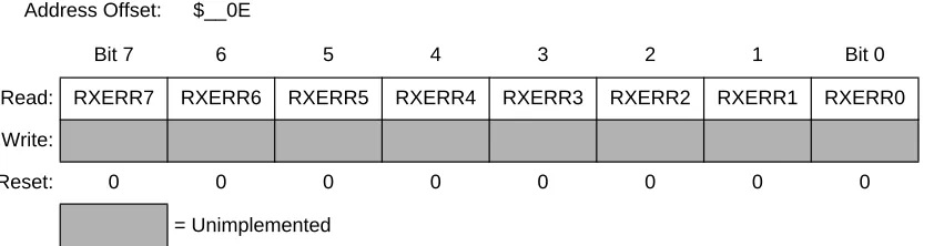
Address Offset: $__0E
Bit 7 6 5 4 3 2 1 Bit 0
Read: RXERR7 RXERR6 RXERR5 RXERR4 RXERR3 RXERR2 RXERR1 RXERR0
Write:
Reset: 0 0 0 0 0 0 0 0
[image:40.612.144.565.118.229.2]= Unimplemented
Figure 3-14 MSCAN Receive Error Counter Register (CANRXERR)
Address Offset: $__0F
Bit 7 6 5 4 3 2 1 Bit 0
Read: TXERR7 TXERR6 TXERR5 TXERR4 TXERR3 TXERR2 TXERR1 TXERR0
Write:
Reset: 0 0 0 0 0 0 0 0
= Unimplemented
[image:40.612.146.562.478.596.2]NOTE: Reading this register when in any other mode other than Sleep or Initialization Mode, may return an incorrect value. For MCUs with dual CPUs, this may result in a CPU fault condition.
NOTE: Writing to this register when in special modes can alter the MSCAN functionality.
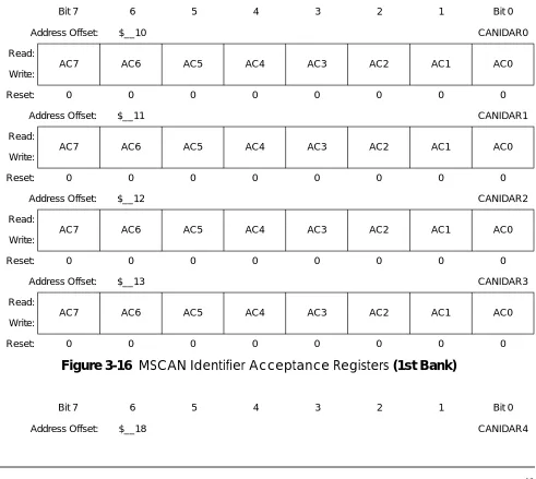
3.3.1.16 MSCAN Identifier Acceptance Registers (CANIDAR0-7)
On reception, each message is written into the background receive buffer. The CPU is only signalled to read the message if it passes the criteria in the identifier acceptance and identifier mask registers
(accepted); otherwise, the message is overwritten by the next message (dropped).
The acceptance registers of the MSCAN are applied on the IDR0 to IDR3 registers3.3.2.1 Identifier Registers (IDR0-3) of incoming messages in a bit by bit manner4.3 Identifier Acceptance Filter. For extended identifiers, all four acceptance and mask registers are applied. For standard identifiers, only the first two (CANIDAR0/1, CANIDMR0/1) are applied.
Bit 7 6 5 4 3 2 1 Bit 0
Address Offset: $__10 CANIDAR0
Read:
AC7 AC6 AC5 AC4 AC3 AC2 AC1 AC0
Write:
Reset: 0 0 0 0 0 0 0 0
Address Offset: $__11 CANIDAR1
Read:
AC7 AC6 AC5 AC4 AC3 AC2 AC1 AC0
Write:
Reset: 0 0 0 0 0 0 0 0
Address Offset: $__12 CANIDAR2
Read:
AC7 AC6 AC5 AC4 AC3 AC2 AC1 AC0
Write:
Reset: 0 0 0 0 0 0 0 0
Address Offset: $__13 CANIDAR3
Read:
AC7 AC6 AC5 AC4 AC3 AC2 AC1 AC0
Write:
[image:41.612.69.560.292.731.2]Reset: 0 0 0 0 0 0 0 0
Figure 3-16 MSCAN Identifier Acceptance Registers(1st Bank)
Bit 7 6 5 4 3 2 1 Bit 0
Read: Anytime
Write: Anytime in Initialization Mode (INITRQ=1 and INITAK=1)
AC7 – AC0 — Acceptance Code Bits
AC7 – AC0 comprise a user defined sequence of bits with which the corresponding bits of the related identifier register (IDRn) of the receive message buffer are compared. The result of this comparison is then masked with the corresponding identifier mask register.
3.3.1.17 MSCAN Identifier Mask Registers (CANIDMR0-7)
The identifier mask register specifies which of the corresponding bits in the identifier acceptance register are relevant for acceptance filtering. To receive standard identifiers in 32 bit filter mode, it is required to program the last three bits (AM2 - AM0) in the mask registers CANIDMR1 and CANIDMR5 to “don’t care”. To receive standard identifiers in 16 bit filter mode, it is required to program the last three bits (AM2 - AM0) in the mask registers CANIDMR1, CANIDMR3, CANIDMR5 and CANIDMR7 to “don’t care”.
Read:
AC7 AC6 AC5 AC4 AC3 AC2 AC1 AC0
Write:
Reset: 0 0 0 0 0 0 0 0
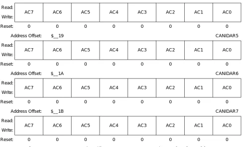
Address Offset: $__19 CANIDAR5
Read:
AC7 AC6 AC5 AC4 AC3 AC2 AC1 AC0
Write:
Reset: 0 0 0 0 0 0 0 0
Address Offset: $__1A CANIDAR6
Read:
AC7 AC6 AC5 AC4 AC3 AC2 AC1 AC0
Write:
Reset: 0 0 0 0 0 0 0 0
Address Offset: $__1B CANIDAR7
Read:
AC7 AC6 AC5 AC4 AC3 AC2 AC1 AC0
Write:
[image:42.612.74.562.48.344.2]Reset: 0 0 0 0 0 0 0 0
Figure 3-17MSCAN Identifier Acceptance Registers(2nd Bank)
Bit 7 6 5 4 3 2 1 Bit 0
Read:
AM7 AM6 AM5 AM4 AM3 AM2 AM1 AM0
Write:
Reset: 0 0 0 0 0 0 0 0
Address Offset: $__15 CANIDMR1
Read:
AM7 AM6 AM5 AM4 AM3 AM2 AM1 AM0
Write:
Reset: 0 0 0 0 0 0 0 0
Address Offset: $__16 CANIDMR2
Read:
AM7 AM6 AM5 AM4 AM3 AM2 AM1 AM0
Write:
Reset: 0 0 0 0 0 0 0 0
Address Offset: $__17 CANIDMR3
Read:
AM7 AM6 AM5 AM4 AM3 AM2 AM1 AM0
Write:
[image:43.612.77.559.51.353.2]Reset: 0 0 0 0 0 0 0 0
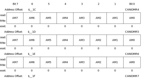
Figure 3-18 MSCAN Identifier Mask Registers(1st Bank)
Bit 7 6 5 4 3 2 1 Bit 0
Address Offset: $__1C CANIDMR4
Read:
AM7 AM6 AM5 AM4 AM3 AM2 AM1 AM0
Write:
Reset: 0 0 0 0 0 0 0 0
Address Offset: $__1D CANIDMR5
Read:
AM7 AM6 AM5 AM4 AM3 AM2 AM1 AM0
Write:
Reset: 0 0 0 0 0 0 0 0
Address Offset: $__1E CANIDMR6
Read:
AM7 AM6 AM5 AM4 AM3 AM2 AM1 AM0
Write:
Reset: 0 0 0 0 0 0 0 0
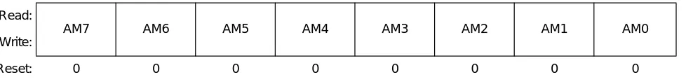
[image:43.612.79.563.406.677.2]Address Offset: $__1F CANIDMR7
Read: Anytime
Write: Anytime in Initialization Mode (INITRQ=1 and INITAK=1)
AM7 – AM0 — Acceptance Mask Bits
If a particular bit in this register is cleared, this indicates that the corresponding bit in the identifier acceptance register must be the same as its identifier bit before a match is detected. The message is accepted if all such bits match. If a bit is set, it indicates that the state of the corresponding bit in the identifier acceptance register does not affect whether or not the message is accepted.
1 = Ignore corresponding acceptance code register bit.
0 = Match corresponding acceptance code register and identifier bits.
3.3.2 Programmer’s Model of Message Storage
The following section details the organization of the receive and transmit message buffers and the associated control registers.
For reasons of programmer interface simplification, the receive and transmit message buffers have the same outline. Each message buffer allocates 16 bytes in the memory map containing a 13 byte data structure.
An additional Transmit Buffer Priority Register (TBPR) is defined for the transmit buffers. Within the last two bytes of this memory map the MSCAN stores a special 16-bit time stamp, which is sampled from an internal timer after successful transmission or reception of a message. This feature is only available for transmit and receiver buffers, if the TIME bit is set (3.3.1.1 MSCAN Control 0 Register
(CANCTL0)).
The Time Stamp register is written by the MSCAN. The CPU can only read these registers.
Read:
AM7 AM6 AM5 AM4 AM3 AM2 AM1 AM0
Write:
[image:44.612.76.565.52.112.2]Reset: 0 0 0 0 0 0 0 0
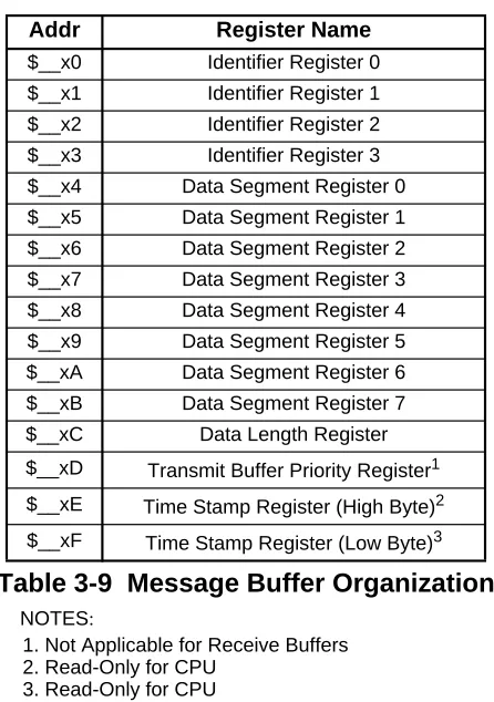
Figure 3-20 shows the common 13 byte data structure of receive and transmit buffers for extended identifiers. The mapping of standard identifiers into the IDR registers is shown inFigure 3-21.
All bits of the receive and transmit buffers are ‘x’ out of reset because of RAM based implementation1. All reserved or unused bits of the receive and transmit buffers are always read ‘x’.
Addr Register Name
$__x0 Identifier Register 0
$__x1 Identifier Register 1
$__x2 Identifier Register 2
$__x3 Identifier Register 3
$__x4 Data Segment Register 0
$__x5 Data Segment Register 1
$__x6 Data Segment Register 2
$__x7 Data Segment Register 3
$__x8 Data Segment Register 4
$__x9 Data Segment Register 5
$__xA Data Segment Register 6
$__xB Data Segment Register 7
$__xC Data Length Register
$__xD Transmit Buffer Priority Register1
NOTES:
1. Not Applicable for Receive Buffers
$__xE Time Stamp Register (High Byte)2
2. Read-Only for CPU
$__xF Time Stamp Register (Low Byte)3
3. Read-Only for CPU
Table 3-9 Message Buffer Organization
NOTES:
1. Exception: The Transmit Priority Registers are “0” out of reset
Register name Bit 7 6 5 4 3 2 1 Bit 0 ADDR
IDR0 Read: ID28 ID27 ID26 ID25 ID24 ID23 ID22 ID21 $__x0
Write:
IDR1 Read: ID20 ID19 ID18 SRR (=1) IDE (=1) ID17 ID16 ID15 $__x1 Write:
IDR2 Read: ID14 ID13 ID12 ID11 ID10 ID9 ID8 ID7 $__x2
Write:
IDR3 Read: ID6 ID5 ID4 ID3 ID2 ID1 ID0 RTR $__x3
Write:
[image:45.612.71.558.489.630.2]= Unused1
Read: Anytime for transmit buffers; only when RXF flag is set for receive buffers (see3.3.1.5 MSCAN Receiver Flag Register (CANRFLG)).
Write: Anytime for transmit buffers when TXEx flag is set (see3.3.1.7 MSCAN Transmitter Flag Register (CANTFLG)) and the corresponding transmit buffer is selected in CANTBSEL (see3.3.1.11 MSCAN Transmit Buffer Selection (CANTBSEL)); unimplemented for receive buffers
Reset: $xx because of RAM based implementation
DSR0 Read: DB7 DB6 DB5 DB4 DB3 DB2 DB1 DB0 $__x4
Write:
DSR1 Read: DB7 DB6 DB5 DB4 DB3 DB2 DB1 DB0 $__x5
Write:
DSR2 Read: DB7 DB6 DB5 DB4 DB3 DB2 DB1 DB0 $__x6
Write:
DSR3 Read: DB7 DB6 DB5 DB4 DB3 DB2 DB1 DB0 $__x7
Write:
DSR4 Read: DB7 DB6 DB5 DB4 DB3 DB2 DB1 DB0 $__x8
Write:
DSR5 Read: DB7 DB6 DB5 DB4 DB3 DB2 DB1 DB0 $__x9
Write:
DSR6 Read: DB7 DB6 DB5 DB4 DB3 DB2 DB1 DB0 $__xA
Write:
DSR7 Read: DB7 DB6 DB5 DB4 DB3 DB2 DB1 DB0 $__xB
Write:
DLR Read: DLC3 DLC2 DLC1 DLC0 $__xC
Write:
NOTES:
1. Unused bits are always read ‘x’
Register name Bit 7 6 5 4 3 2 1 Bit 0 ADDR
IDR0 Read: ID10 ID9 ID8 ID7 ID6 ID5 ID4 ID3 $__x0
Write:
IDR1 Read: ID2 ID1 ID0 RTR IDE (=0) $__x1
Write:
IDR2 Read