Fiona Mair Bain
A Thesis Submitted for the Degree of PhD at the
University of St. Andrews
2010
Full metadata for this item is available in Research@StAndrews:FullText
at:
https://research-repository.st-andrews.ac.uk/
Please use this identifier to cite or link to this item:
http://hdl.handle.net/10023/1698
This item is protected by original copyright
Thesis presented for the degree of
Doctor of Philosophy
to the University of St Andrews
by
Fiona Mair Bain
May 2010
The J. F. Allen Physics Research Laboratories School of Physics and Astronomy
University of St Andrews North Haugh
I, Fiona Mair Bain, hereby certify that this thesis, which is approximately thirty-five
thousand words in length, has been written by me, that it is the record of work carried
out by me and that it has not been submitted in any previous application for a higher
degree.
I was admitted as a research student in October 2006 and as a candidate for the degree
of Doctor of Philosophy in October 2006; the higher study for which this is a record
was carried out in the University of St Andrews between 2006 and 2010.
Date: Signature of candidate:
I hereby certify that the candidate has fulfilled the conditions of the Resolution and
Regulations appropriate for the degree of Doctor of Philosophy in the University of St
Andrews and that the candidate is qualified to submit this thesis in application for that
degree.
In submitting this thesis to the University of St Andrews I understand that I am giving
permission for it to be made available for use in accordance with the regulations of
the University Library for the time being in force, subject to any copyright vested in
the work not being affected thereby. I also understand that the title and the abstract
will be published, and that a copy of the work may be made and supplied to any bona
fide library or research worker, that my thesis will be electronically accessible for
personal or research use unless exempt by award of an embargo as requested below,
and that the library has the right to migrate my thesis into new electronic forms as
required to ensure continued access to the thesis. I have obtained any third-party
copyright permissions that may be required in order to allow such access and
migration, or have requested the appropriate embargo below.
The following is an agreed request by candidate and supervisor regarding the
electronic publication of this thesis:
Access to Printed copy and electronic publication of thesis through the University of
St Andrews.
Date: Signature of candidate:
Lasers find a wide range of applications in many areas including photo-biology,
photo-chemistry, materials processing, imaging and telecommunications. However,
the practical use of such sources is often limited by the bulky nature of existing
systems. By fabricating channel waveguides in solid-state laser-gain materials more
compact laser systems can be designed and fabricated, providing user-friendly
sources. Other advantages inherent in the use of waveguide gain media include the
maintenance of high intensities over extended interaction lengths, reducing laser
thresholds.
This thesis presents the development of Yb:tungstate lasers operating around 1µm in
waveguide geometries. An Yb:KY(WO4)2 planar waveguide laser grown by liquid
phase epitaxy is demonstrated with output powers up to 190 mW and 76 % slope
efficiency. This is similar to the performance from bulk lasers but in a very compact
design. Excellent thresholds of only 40 mW absorbed pump power are realised. The
propagation loss is found to be less than 0.1 dBcm-1 and Q-switched operation is also
demonstrated.
Channel waveguides are fabricated in Yb:KGd(WO4)2 and Yb:KY(WO4)2 using
ultrafast laser inscription. Several of these waveguides lase in compact monolithic
cavities. A maximum output power of 18.6 mW is observed, with a propagation loss
of ~2 dBcm-1. By using a variety of writing conditions the optimum writing pulse
energy is identified. Micro-spectroscopy experiments are performed to enable a fuller
understanding of the induced crystal modification. Observations include frequency
shifts of Raman lines which are attributed to densification of WO2W bonds in the
crystal.
Yb:tungstate lasers can generate ultrashort pulses and some preliminary work is done
to investigate the use of quantum dot devices as saturable absorbers. These are shown
to have reduced saturation fluence compared to quantum well devices, making them
particularly suitable for future integration with Yb:tungstate waveguides for the
During this PhD I have been privileged to receive great support from many
colleagues, family and friends, and so there are various people I’d like to thank.
Special thanks must go Tom Brown who’s been an excellent supervisor, supporting
me at every stage; giving me opportunities to present my work; encouraging me
through the writing process; and being the only person (so far) to have read through
my entire thesis! His feedback in this has been extremely helpful. Particular thanks
must also go to Alexander Lagatsky. His help and advice in the lab have been
invaluable, and the work presented here would not have been accomplished without
him.
I would also like to thank all other group members past and present: Ben, Chris,
Christine, Craig, Douglas, Eddie, Flavio, Gajendra, Klaus, Mario, Ronan and Wilson,
for their advice on various pieces of equipment, listening to and giving feedback on
my talks, and for useful discussions on various topics. Thanks go to all my
collaborators in Minsk, Heriot Watt and Madrid, and especially Robert, Dani and
Wagner with whom I’ve had personal contact. Thanks are due to all the guys from the
workshop for various mounts that they’ve made for me, thanks to Scott for dealing
with all the deliveries, thanks to the secretaries for all their administration work, and
thanks to Mike and Cameron for keeping me safe in the building!
Thanks to my many friends in the department, besides those mentioned previously,
who have been a support throughout my studies here: Jill, Janelle, Lani, Maria, Claire,
Areti, Anna Chiara and Sarah. Also thanks to Svetlana, from the Physics department
in Dundee, who has been an excellent conference roommate, has helped me prepare
and practice for most of my talks, and has provided useful quantum dot discussions.
Thanks also to my MSc friends, particularly Kamol, Klearchos, Shailen and Wei, who
have been an incredibly useful resource by reminding me of basic photonics! Thanks
to my hall and housemates over the years who have been fantastic to live with: Jill
department, but the best fiancé who has read almost as much of my thesis as Tom has!
Du bist der Beste!
Finally I’d like to thank my family, who have supported me from the beginning in
everything I’ve ever done. Duncan, Jenny and Alistair are a great set of siblings, and
Alistair deserves special mention for working through a derivation of the waveguide
equation. Mum and Dad have always been a great influence and encouragement, and
without them none of this would have been possible. I’d like to thank them both for
listening to me practice various conference talks again and again. Thanks also to Mum
for reading and commenting on my abstract, conclusion and other sections of my
thesis, and to Dad for reading and correcting my first year report, and I know he
In loving memory of Dad
Dr Robert Bruce Vorlich Bain
Time Passes
Just sitting here in contemplation Aging slowly, measured and unseen, While mind and time both race ahead Far from those places I have been
Our fleeting life goes by so fast Like an arrow’s murderous flight
Straight and true, unerringly Toward the target in its sight
Or like a comet in the night Streaking through the starrysky,
Furiously, at breakneck speed Before its fading light must die
Neither turning nor yet slowing It seeks always to find its mark
Ever on, by fire consumed, Towards a future stark and dark
And like that comet, so are we However much we speed our span
However fast to those near by It’s as a flash, since time began
We cannot slow it, cannot turn it All we can is seize the day Cherish, hold, squeeze every moment
Before it too must fly away
For however fast we run Or however high we climb We can never long outpace Those slowly flowing sands of time
Contents
Declarations ii
Abstract iv
Acknowledgements v
Contents viii
Glossary of Symbols xii
Glossary of Acronyms xvi
Publications xviii
Chapter 1 – Introduction and Background 1
1.1 Half a Century of the Laser 1
1.2 The Ytterbium Ion 2
1.3 Double Tungstates as Laser Hosts 3
1.3.1 Double Tungstate Crystal Structure 4
1.3.2 Thermal Properties 7
1.3.3 Optical Properties 7
1.3.4 Absorption and Emission Properties 9
1.3.5 Summary of Previous Lasing Performance 10
1.4 The Quasi-Three-Level Laser 11
1.5 Continuous and Pulsed Lasing 12
1.5.1 Q-switching 13
1.5.2 Mode Locking 14
1.6 Waveguide Theory 17
1.7 Waveguide Fabrication 23
1.8 Conclusion and Thesis Synopsis 26
1.9 References 27
Chapter 2 – Experimental Techniques 38
2.1 Introduction 38
2.2 Ultrafast Laser Inscription 38
2.3 Laser Design and Performance 39
2.3.2 Asymmetric Z-fold Cavities 40
2.3.3 Waveguide Cavities 41
2.3.4 Absorbed Pump Power 42
2.3.5 Laser Performance 44
2.3.6 Caird Plots 46
2.4 Waveguide Loss Measurements 46
2.4.1 Transmission Method 48
2.4.2 Luminescence Decay Method 49
2.5 Conclusions 50
2.6 References 51
Chapter 3 – Quantum Dot Saturable Absorbers 52
3.1 Introduction 52
3.2 Quantum Confinement 53
3.3 Quantum Dots versus Quantum Wells 54
3.4 Yb:KYW Laser Mode Locked with a QD-SESAM 56
3.4.1 Description of the QD-SESAM 56
3.4.2 Laser Cavity and Mode-locked Performance 57
3.5 SESAM Characterisation 58
3.5.1 Modelling of Fluence-Dependent SESAM Reflectivity 58
3.5.2 Experimental Set-up for Measuring Non-linear Reflectivity 61
3.5.3 Characterisation of QD-SESAM, s-571-80QD 63
3.5.4 Characterisation of QD-SESAM, QD-5-233 64
3.6 Channel Waveguide in a Quantum Dot Doped Glass 65
3.6.1 Quantum Dot Sample 65
3.6.2 Waveguide Writing Conditions 66
3.6.3 Waveguide Loss Measurements 66
3.7 Conclusions and Future Outlook 68
3.8 References 69
Chapter 4 – Yb:KYW LPE-grown Planar Waveguide Laser 71
4.1 Introduction 71
4.3 Lasing from Yb:KYW 100 µm Yb:KYW Layer 73
4.4 Lasing from 14 µm Yb:KYW Planar Waveguide 77
4.5 Q-switching from 14 µm Yb:KYW Planar Waveguide 82
4.6 Partially Unstable 14 µm Yb:KYW Planar Waveguide Laser 85
4.7 Conclusions and Future Work 89
4.8 References 91
Chapter 5 – Yb:tungstate Channel Waveguide Lasers 93
5.1 Introduction 93
5.2 Sample Description and Writing Conditions 93
5.3 Experimental Procedures 95
5.3.1 Identifying Crystal Modification and Guiding Regions 95
5.3.2 Laser Cavity 96
5.3.3 Loss Measurements 97
5.4 Channel Waveguide Results 98
5.4.1 Yb:KGdW 98
5.4.1.1 Guiding, Lasing and Losses in Yb:KGdW with E||a 99
5.4.1.2 Guiding, Lasing and Losses in Yb:KGdW with E||b 105
5.4.2 Yb:KYW 108
5.4.2.1 Guiding, Lasing and Losses in Yb:KYW with E||a 108
5.4.2.2 Guiding, Lasing and Losses in Yb:KYW with E||b 109
5.5 Conclusions and Future Work 116
5.6 References 117
Chapter 6 – Micro-spectroscopy of Channel Waveguides 119
6.1 Introduction 119
6.2 Experimental Set-up 120
6.3 Double Tungstate Raman Spectroscopy 121
6.4 Yb:KGdW Micro-spectroscopy 123
6.4.1 Analysed Structures 123
6.4.2 Micro-luminescence Results 124
6.4.3 Micro-Raman Results 126
6.5.1 Analysed Structures 130
6.5.2 Micro-luminescence Results 131
6.5.3 Micro-Raman Results 133
6.6 Conclusions and Future Outlook 136
6.7 References 138
Chapter 7 – Conclusions 140
7.1 Thesis Summary 140
7.2 Future Work 145
7.3 References 147
Appendix A – Tables of Inscribed Waveguides 148
Yb:KGdW Writing Conditions 148
Glossary of Symbols
|| Parallel
α Gain/loss co-efficient
αdB Gain/loss co efficient in dB
β Angle between a and c crystallographic axes
δ Round trip cavity loss
δcoupl Coupling loss
δdB Loss in dB
δins Insertion loss
δlaunch Launch efficiency
δns Non-saturable losses
δprop Propagation loss
η Slope efficiency
η0 Intrinsic slope efficiency
ηp Pump quantum efficiency
θ Angle, where subscripts i, r and t represent incidence, reflection
and transmission
θc Critical angle
λ Wavelength, subscripts of p and l represent pump and lasing
wavelengths respectively
π Pi, 3.1416
σ Cross section, where subscripts a and e represent absorption
and emission
σx2 Second moment of a beam along x
∆τ Pulse duration
τrec Recovery time
τrt Round trip cavity time
τupp Upper state life-time
υp Phase velocity of light
φ Goos-Hänchen phase shift
φam Angle between a and Nm
χ(i) ith order susceptibility
∆ω Full spectral range of cavity
a, b, c Crystallographic axes
a Waveguide asymmetry parameter
aij Thermal expansion co-efficient
A Single pass absorption
b Normalised guide index
c Speed of light, 2.998×10⁻⁸ ms-1
dguide Waveguide thickness
e Euler’s number, 2.718
E Energy, where subscript p denotes pulse energy
E Electric field
∆E Energy difference
f Fractional population of level
f1(0) Fractional population of upper lasing level
frep Repetition rate
F Represents L = 3
F Fluence, where subscripts sat, p, pGauss and 0 represent
saturation, pulse, Gaussian pulse and peak saturation
respectively
g Degeneracy
h Planck’s constant, 6.626×10⁻³⁴ Js
I Intensity
J Total angular momentum
k Wavenumber, equal to 2π/λ
kB Boltzmann’s constant
L Orbital angular momentum
L Length
m Mode number
me Effective mass of electron
M 2 Measure of beam quality
neff Effective refractive index of a waveguide
n2 Nonlinear refractive index
Nm, Ng, Np Principal optical axes
N Population of given state
N0(3) Population of lower lasing level
p Constant which depends on pulse shape
Pabs Absorbed pump power
Pabs,th Threshold absorbed pump power
Pi Incident power
Pout Output power
Pt_bulk Power transmitted through bulk material
Pt_guide Power transmitted through waveguide
Q Quality of a cavity
r Radius of waveguide core
rl Normalised laser mode
rp Normalised pump mode
R Reflectivity, subscripts s and pi denote sigma and pi
polarisations
∆R Modulation depth
RF Fresnel reflection
Rlin Reflectivity under low light intensity
Rns Saturated reflectivity
Rp Pumping rate
Rp,th Threshold pumping rate
s, p, d, f Angular momentum quantum numbers 0, 1, 2 and 3
S Spin angular momentum
S Saturation parameter
T Temperature
TF Transmission of end facets
Tobj Transmission of objective
TOC Transmission of output coupler
t Time
v Molecular vibration, subscripts are described in text
V Normalised frequency Parameter
w Beam waist (radius at e-2), where subscripts l and p denote
lasing and pump modes and 0 denotes beam waist at focus
x, y, z Spatial co-ordinates
X1′, X2′, X3′ Thermal expansion co-efficients in the principal system
Glossary of Acronyms
2D Two dimensional
3D Three dimensional
at. Atomic
A Monovalent alkali-metal cation
ABCD Matrix elements for optical ray matrix
Al Aluminium
AL Achromatic lens
AFM Atomic Force Microscopy
ASE Amplified spontaneous emission
CCD Charge coupled device
CW Continuous wave
DBR Distributed Bragg reflector
DM Dichroic mirror
GaAs Gallium Arsenide
Gd Gadolinium
HT High transmission
HR High reflector
HWP Half-waveplate
IR Infrared
K Potassium
KLM Kerr-lens mode locking
LiF Lithium fluoride
Ln Lanthanide
LPE Liquid phase epitaxy/epitaxially
Lu Lutetium
M Mirror
MBE Molecular beam epitaxy
N.A. Numerical aperture
Nd Neodymium
O Oxygen
OC Output coupler
OSA Optical spectrum analyser
PbS Lead sulfide
PBS Polarising beam-splitter
PLD Pulsed laser deposition
R Trivalent metal or rare-earth cation
RF Radio frequency
SBR Saturable Bragg reflector
SESAM Semiconductor saturable absorber mirror
SF10 Fused silica prism
SIMS Secondary ion mass spectroscopy
Sm Samarium
TE Transverse electric field
TEM Transmission electron microscopy
TEM00 Fundamental mode Gaussian beam
Ti Titanium
TM Transverse magnetic field
TSSG Top-seeded solution growth
QD Quantum dot
QW Quantum well
QWP Quarter waveplate
ULI Ultrafast laser inscription/inscribed
W Tungsten
(WO4)2 Double tungstate
Y Yttrium
YAG Yttrium aluminium garnet
Yb Ytterbium
Publications
Journal Publications
1. “Ultrafast laser inscribed Yb:KGd(WO4)2 and Yb:KY(WO4)2 channel
waveguide lasers," F. M. Bain, A. A. Lagatsky, R. R. Thomson, N. D.
Psaila, N. V. Kuleshov, A. K. Kar, W. Sibbett, C. T. A. Brown, Opt. Exp.
17, 22417-22422 (2009)
2. “Continuous-wave and Q-switched operation of a compact,
diode-pumped Yb3+:KY(WO4)2 planar waveguide laser”, F. M. Bain, A. A.
Lagatsky, S. V. Kurilchick, V. E. Kisel, S. A. Guretsky, A. M. Luginets,
N. A. Kalanda, I. M. Kolesova, N. V. Kuleshov, W. Sibbett and C. T. A.
Brown, Opt. Exp. 17, 1666-1670 (2009)
3. “Low-loss quantum-dot-based saturable absorber for efficient
femtosecond pulse generation” A. A. Lagatsky, F. M. Bain, C. T. A.
Brown, W. Sibbett, D. A. Livshits, G. Erbert and E. U. Rafailov, Appl.
Phys. Lett. 91, 231111-231113, (2007)
4. “Micro-spectroscopy of ultrafast laser inscribed channel waveguides in
Yb:tungstate crystals,” F. M. Bain, W. F. Silva, A. A. Lagatsky, R. R.
Thomson, N. D. Psaila, A. K. Kar, W. Sibbett, D. Jaque, C. T. A. Brown,
submitted for publication in Appl. Phys. Lett., June 2010
5. “Lasing action at around 1.9 µm from an ultrafast laser inscribed
Tm-doped glass waveguide,” F. Fusari, R. R. Thomson, G. Jose, F. M.
Bain, A. A Lagatsky, N. D. Psaila, A. K. Kar, A. Jha, W. Sibbett, C. T. A.
Conference Proceedings
1. “Optical Waveguides in Glasses doped with Lead Sulfide Quantum Dots”,
A. M. Malyarevich, K. V. Yumashev, A. A. Lagatsky, F. M. Bain, C. T.
A. Brown, W. Sibbett, R. R. Thomson, A. K. Kar, A. A. Anushchenko, A.
A. Zhilin, A. A. Lipovskii, Physics, Chemistry and Application of
Nanostructures, 140-143 (2009)
2. “Diode-pumped femtosecond Yb:KYW laser incorporating a quantum-dot
saturable absorber”, A. A. Lagatsky, F. Bain, C. T. A. Brown, W. Sibbett,
D. A. Livshits, G. Erbert, E. U. Rafailov, 2007 Conference of Laser and
Electro-Optics/Quantum Electronics and Laser Science Conference
(CLEO/QELS 2007), 1-5, 472-473 (2007)
3. “High-power Kerr-lens mode-locked ytterbium lasers” F. M. Bain, A. A.
Lagatsky, C. T. A. Brown and W. Sibbett, Solid State Lasers XV11:
Technology and Devices, Proc. of SPIE, 6871, L68712, 2008
Presented Talks
1. “Micro-Luminescence and Micro-Raman Mapping of Ultrafast Laser
Inscribed Yb:KGd(WO4)2 and Yb:KY(WO4)2 Channel Waveguides,” F.
M. Bain, A. A. Lagatsky, W. F. Silva, D. Jaque, R. R. Thomson, N. D.
Psaila, A. K. Kar, W. Sibbett, C. T. A. Brown, presented by F. M. Bain,
presentation number CMQ7 at CLEO, San Jose, California, May 2010
2. “Diode-pumped ytterbium-doped double tungstate waveguide lasers,” F.
M. Bain, A. A. Lagatsky, W. Sibbett, C. T. A. Brown, presented by F. M.
Bain at SU2P symposium, Glasgow, March 2010
3. “Diode-pumped double-tungstate waveguide lasers”, F. M. Bain, A. A.
Bain at the University of Twente, Enschede, The Netherlands, October
2009
4. “Diode-pumped double-tungstate waveguide lasers”, F. M. Bain, A. A.
Lagatsky, C. T. A. Brown and W. Sibbett, invited talk presented by C. T.
A. Brown at the 18th International Laser Physics Workshop (LPHYS ’09)
at ICFO, Barcelona, Spain, July 2009
5. “Yb:KGd(WO4)2 channel waveguide laser fabricated by ultrafast laser
writing”, F. M. Bain, A. A. Lagatsky, W. Sibbett, C. T. A. Brown, R. R.
Thomson, N. D. Psaila, A. K. Kar and N. V. Kuleshov, presented by F. M.
Bain, presentation number CJ7.3 at CLEO Europe, Munich, Germany,
June 2009
6. “Diode-pumped Yb:KYW waveguide lasers” F. M. Bain, A. A. Lagatsky,
S. V. Kurilchik, V. E. Kisel, S. A. Guretsky, A. M. Luginets, I. M.
Kolesova, C. T. A. Brown, W. Sibbett and N. V. Kuleshov, presented by
F. M. Bain at 3rd EPS-QEOD Europhoton Conference, Paris, France,
September 2008
7. “1 micron and 1.3 micron femtosecond lasers mode-locked using
quantum-dot-based saturable absorbers”, F. M. Bain, A. A. Lagatsky, C.
T. A. Brown, W. Sibbett, D. A. Livshits, A. E. Zhukov, V. M. Ustinoc, E.
U. Rafailov, presented by F. M. Bain at CLEO Europe, Munich, Germany,
So what you like, let you decide And don’t let fashions fetter
It matters not if it is new It matters if it’s better
And disregard the taunts and barbs Of ‘It’s been done before’ For so have life and sex and love
Yet still we do them more
Chapter 1
Introduction and Background
1.1 Half a Century of the Laser
Fifty years have passed since the first demonstration of the laser by Maiman in 1960
[1], and during this time the world has been transformed by the advances that this
light source, which was once described as a “solution waiting for a problem” [2], has
brought. As a coherent light source it has wide-ranging relevance to various
applications; for example in the fields of holography [3] and interferometry [4], where
lasers have been used in CD players [5, 6], lithography [7], optical sensing [8] and
LIDAR [9]. A further property of interference is that, given a large enough
bandwidth, ultrashort pulses can be generated and pulses as short as 6.5 fs
(6.5×10⁻¹⁵ s) have now been produced directly from a laser [10]. The creation of
broadband, ultrashort pulses has revolutionised many disciplines, from photo-biology,
photo-chemistry [11-15] and medicine [16-18] to materials processing [19, 20] and
telecommunications [21]. However, few of these applications have made use of the
ruby laser, which was the laser initially built by Maiman. All of these various exciting
techniques have relied on the steady but intensive efforts of researchers over the past
five decades to vary the properties of available lasers; both in terms of fundamental
physical aspects, such as available wavelength [22-28], efficiency [29, 30], output
power [31-33], threshold [34, 35], pulse duration [10, 36-39], pulse energy [40] and
repetition rate [41]; and also with regard to design, as more compact laser sources are
inherently lighter, more practical and user-friendly [42, 43].
The aim of the research described in this thesis has been the development of compact
and efficient lasers at wavelengths around 1 µm. Ytterbium-doped crystalline
materials have been chosen as gain media due to their excellent material and
spectroscopic properties, which have previously been shown to lase in a bulk
geometry with excellent efficiencies and to be capable of producing ultrashort pulses
[44]. Their high absorption and emission cross sections also make them suitable for
goal of this work was the fabrication and lasing of waveguides based on these
materials which enable ultracompact monolithic cavities with relatively low
thresholds to be constructed.
The topics investigated in this thesis are all now introduced, beginning with a
discussion of the ytterbium ion and its suitability as a dopant for producing ultrashort
pulses with a wavelength around 1 µm. Of equal importance to the chosen dopant is
the host crystal, and details of the hosts explored during these experiments are also
presented. This topic leads on to a description of the quasi-three-level laser, which is
followed by a brief review of continuous wave (CW), Q-switched and mode-locked
regimes. Finally the theory of optical waveguides and their applications to laser
design are discussed briefly together with some fabrication techniques, and a synopsis
of the remaining thesis is presented.
1.2 The Ytterbium Ion
Ytterbium is a rare-earth lanthanide element, generally found as the trivalent cation
Yb3+. It was discovered in 1878 [45] and first used as an ion for a laser transition in
1965 [25]. However, its potential as a laser ion was largely ignored until a suitable
diode pump became available in 1990 [46]. Ytterbium’s electron configuration is
described by [Xe] 6s2 4f14, with two valence electrons in the 6s orbital and one in the
4f orbital, while its cation has an ionic radius of 87 pm and the electron configuration
[Xe] 4f13. This means it lacks one electron to complete its valence shell. The 4f
sub-shell is shielded by the complete 5s and 5p sub-sub-shells.
The 13 electrons in the outer sub-shell, 4f, of Yb3+ consist of six pairs of electrons in
six of the orbitals, plus one final unpaired electron in the seventh orbital. Thus the
total spin angular momentum, S, is a half. Multiplicity is given by 2S+1 [47] and
consequently the multiplicity of Yb3+ is 2, giving rise to a doublet term. The total
orbital angular momentum, L, is 3. The total angular momentum, J, combines the
electrons’ orbital and spin angular momenta by considering their relative orientations.
The values of J are given by the series J = L + S, L + S - 1, …|L - S| [48], and thus for
levels of the ytterbium ion are given by the terms 2F7/2 and 2F5/2, where terms are
written in the standard form 2S+1LJ, and L = 3 is represented by the symbol F.
According to Hund’s third selection rule, if the outer shell is over half-full then the
lowest energy level has the highest total angular momentum [49]. Therefore 2F7/2 is
the ground state of Yb3+ whilst 2F5/2 is the excited state, and these are separated by
approximately 10000 cm-1 [50] (the precise value will depend upon the ion’s host). A
material containing Yb ions will thus absorb and emit around 1 micron.
The ytterbium ion is therefore described by a simple two-level system, and the
absence of other energy levels is advantageous for lasing as losses due to excited state
absorption, upconversion and concentration quenching are removed even at higher
doping levels [51, 52]. Other advantages of ytterbium when used as the active laser
ion include: strong absorption and emission cross sections particularly in the double
tungstate hosts; strong absorption around 980 nm making it highly suitable for diode
pumping with readily available InGaAs laser diodes; a small Stokes shift which leads
to high slope efficiencies; and inhomogeneous broadening in many hosts which
provides a broad emission bandwidth suitable for femtosecond pulse generation.
These points outline the attractiveness of Yb3+ as an active laser ion, and particularly
the suitability of this ion for creating compact and efficient lasers. There are numerous
examples of lasing from various Yb-doped materials in the literature, with many
reporting excellent efficiencies and ultrashort pulses [53-67]. Additional benefits can
include using ytterbium as a sensitizer for many other rare-earth ions [57, 68, 69].
1.3 Double Tungstates as Laser Hosts
Equally important to the choice of ion when developing a good laser material is the
choice of a suitable host. In this thesis crystalline hosts have been chosen. Although
more expensive to fabricate than glasses, the advantages of crystals in terms of
strength, homogeneity, thermal conductivity and large cross sections – leading to
lower thresholds – can more than outweigh the greater cost. Furthermore, with the
correct choice of host, it is possible to obtain broad and smooth emission bandwidths
Double tungstates were chosen as hosts in this experimental work. These are a group
of crystals with the formula AIRIII(WO4)2, where A is a monovalent alkali-metal
cation, and R is a trivalent metal or rare-earth cation. They are biaxial crystals, with
strong χ(2) and χ(3) nonlinearies, making them suitable for second harmonic generation
and stimulated Raman scattering applications [70]. They also provide broad emission
bandwidths making them suitable hosts for the generation of ultrashort pulses.
KGd(WO4)2 (KGdW), KY(WO4)2 (KYW) and KLu(WO4)2 (KLuW) are the double
tungstates which have attracted most attention as crystalline laser host materials [56,
57, 65, 67, 71] .
Two of these double tungstates are used as host materials in this thesis – KGdW and
KYW – and these have all been grown by our collaborators in Minsk, Belarus1 using a
modified Czochralski method [72]. This technique (also known as the top-seeded
solution growth (TSSG)) consists of melting the constituents of the crystal into a
crucible at a high temperature, above the saturation temperature. The melt can be left
for several hours or days to ensure homogeneity and good optical quality of the
crystal. The melt is then gradually cooled to the saturation temperature. A seed crystal
is then introduced and crystal growth begins, with an orientation matching that of the
seed. As growth continues the crystal is slowly rotated and pulled from the melt.
Meanwhile the melt is gradually cooled to ensure the solution remains supersaturated.
For growth of Yb:KGdW and Yb:KYW the K2W2O7 solvent is generally chosen [73]
or K2WO4 [70] can alternatively be used.
1.3.1 Double Tungstate Crystal Structure
Both KGdW and KYW are monoclinic crystals which can be described either by the
C2/c space group, or the I2/c space group. In crystallography C2/c notation is
generally preferred, however the parameters associated with I2/c space group are
those used throughout this thesis. This is due to these parameters comparing well with
the morphology of the crystals. Most of the data presented, such as absorption and
emission spectra and pump and lasing polarisations correspond to the crystallographic
1
axes as defined for the I2/c space group. However, it is possible to convert between
the two using the transformations:
= = − = −
a* a + c
b* b
c* c
where * represents the C2/c notation. A diagram illustrating this is shown in fig. 1.1.
The unit cell parameters are quoted many times in the literature, and typical values are
shown in table 1.1 where good agreement can be seen between the various sources.
a
b = -b*
c
c*
a*
[image:27.595.199.395.296.428.2]*
Fig. 1.1. Relative orientations of crystallographic a, b and c axes in different space group notations.
Unit cell parameters Reference
a (nm) b (nm) c (nm) β (°)
0.8095 1.043 0.7588 94 [57]
0.8098 1.0417 0.7583 94.43 [74] as quoted in [75]
0.8084 1.0374 0.7582 94.41 [75]
0.8122 1.0426 0.7587 94.06 [76]
a* (nm) b* (nm) c* (nm) β* (°)
K
G
d
W
1.0652 1.0374 0.7582 130.80 [75]
a (nm) b (nm) c (nm) β (°)
0.805 1.035 0.754 94 [57, 77]
a* (nm) b* (nm) c* (nm) β* (°)
K
Y
W
1.064 1.035 0.754 130.5 [77, 78]
Table 1.1. Unit cell parameters for KGdW and KYW single crystals, as quoted in literature.
[image:27.595.91.505.483.730.2]The potassium, gadolinium and yttrium atoms occupy 4e Wyckoff positions, whilst
tungsten and oxygen occupy 8f Wyckoff positions. More data regarding the atomic
co-ordinates of the specific atoms can be found in [75]. The crystallographic structure
of KGdW is shown in fig. 1.2. KYW’s structure is identical except that yttrium
replaces the gadolinium. When doping with a lanthanide, the trivalent metal is
replaced with the active doping ion, and so for ytterbium doping the ytterbium ion
replaces the gadolinium or yttrium. The ionic radii of these cations are [79]:
Gd3+: 93.8 pm
Y3+: 90.0 pm
Yb3+: 86.8 pm
As the ionic radii of these lanthanides are all similar, good quality crystals can be
[image:28.595.95.501.378.718.2]grown [75].
1.3.2 Thermal Properties
The thermal expansion co-efficients in the principal system, X1′, X2′, X3′, for KGdW
[75] and KYW [80], together with the orientation of these vectors are shown below:
KGdW KYW
( )
610.64 0 0
0 2.83 0 10
0 0 23.44
ij
a −
= ×
K-1
( )
611.0 0 0
0 1.9 0 10
0 0 17.8
ij
a −
= ×
K-1
a
X
2'
c
168
°
X
1'
X
3'
8
°
a
X
2'
c
171.43
°
X
1'
X
3'
12.32°
Fig. 1.3. Axes of thermal expansion co-efficients relative to crystallographic axes for (a) KGdW and
(b) KYW.
Clearly the largest expansion is close to the crystallographic a axis, whilst the b axis
experiences considerably less thermal expansion. The thermal conductivity of these
crystals is relatively low, at only around 3 Wm-1K-1 [81]. However, the low quantum
defect in these crystals when doped with Yb3+ helps to circumvent this problem.
1.3.3 Optical Properties
The double tungstates are characterised by relatively high refractive indices of
around 2. They are also highly anisotropic due to their large crystal anisotropy with
three principal optical axes, Nm, Ng and Np, which have refractive indices of nm, ng
and np respectively. A range of values for these important parameters exist in the
literature and a summary of these results are given in table 1.2 where the orientation
[image:29.595.88.500.177.413.2]isostructural the refractive index increase of KYW and KGdW is linear with Yb3+
doping concentration [82].
KGdW
[83]
KGdW [84] KGdW [85] KYW
[77]
KYbW
[86]
λ (nm) 1060 532 1546 532 1060 1546 1064 632.8
ng 2.033 2.1091 2.0385 2.1187 2.0610 2.0514 2.0507 2.12
nm 1.986 2.0686 2.0028 2.0627 2.0103 1.9819 2.0065 2.06
np 1.937 2.0352 1.9741 2.0307 1.9819 1.9718 1.9688 2.03
φcg 20° 19.3° 21.5° 17.5° 19°
[image:30.595.224.374.335.464.2]φam 24° 15.3° 17.1° 13.5° 16°
Table 1.2. Principal optical axes refractive indices and axes orientation of double tungstates.
a
c
N
mN
gN
pFig. 1.4. Orientation of principal optical axes of double tungstates.
The nonlinear refractive index, n2, is very important in a laser crystal. It can
sometimes be detrimental to lasing performance, by causing optical breakdown and
limiting the available output power, but it can also be advantageous as it is necessary
for ultrashort pulse generation using Kerr-lens mode locking (KLM). Values for n2
are notoriously difficult to determine and contain large errors in their stated value.
Nonetheless it is agreed that the double tungstates are characterised by relatively large
values of n2 where Yb:KGdW has been quoted to have an n2 of between
~20x10-16 cm2W-1 to 25x10-16 cm2W-1 along Nm, and ~15x10-16 cm2W-1 along Np [87,
88]. In Yb(5 %):KYW values of 19x10-16 cm2W-1 along Nm and 15x10-16 cm2W-1
along Np have been reported [88]. These values are all significantly higher than n2 of
Ti:sapphire at 3.1x10⁻¹⁶ m2W-1 [89].
φam
1.3.4 Absorption and Emission Properties
Some of the most important characteristics of a laser material are its absorption and
emission properties. As mentioned in section 1.2, the ytterbium ion has a simple
electronic structure with only two sublevels, but the values of the Stark levels within
these sublevels are determined by the crystal field of the host and are illustrated in
fig. 1.5.
0 cm-1
163 cm-1
385 cm-1
535 cm-1
10188 cm-1
10471 cm-1
10682 cm-1
2 F5/2 2 F7/2 1 2 3 4 5 6 7
Yb:KGdW
0 cm-1
169 cm-1
407 cm-1
568 cm-1
10187 cm-1
10476 cm-1
10695 cm-1
2 F5/2 2 F7/2 1 2 3 4 5 6 7
Yb:KYW
Fig. 1.5. Stark energy levels for Yb:KGdW and Yb:KYW [90]. These values correspond to a
temperature of 77 K.
880 920 960 1000 1040 1080 0 1 2 3 4 5 Ellc C ro ss s ec ti o n ( 1 0 -2
0 c
m 2 ) Wavelength (nm) 0 2 4 Ellb 0 5 10 15 20 25 30 Abs. Ella Em.
880 920 960 1000 1040 1080 0 1 2 3 Ellc C ro ss s ec ti o n ( 1 0 -2
0 c
m 2 ) Wavelength (nm) 0 2 4 Ellb 0 5 10 15 Abs. Em. Ella
Fig. 1.6. Absorption and emission cross sections for (a) Yb:KGdW and (b) Yb:KYW. Measurements
performed by our collaborators in Minsk.
E||a E||a
E||b E||b
E||c E||c
[image:31.595.99.491.468.720.2]In fig. 1.6 the absorption and emission cross sections as a function of wavelength are
illustrated. These measurements were made by our collaborators in Minsk. As can be
expected from the crystal structure, the absorption and emission spectra are highly
anisotropic, where E||a has the strongest absorption and emission cross sections,
although all axes are characterised by high cross sections when compared to many
other laser materials. The absorption peak for E||a is found at 981.2 nm, which
overlaps well with the emission from commercially available InGaAs laser diodes
[46]. This is an inherent advantage of ytterbium lasers, enabling compact and efficient
laser pumping. The high emission cross sections and broad emission bandwidths are
suitable for supporting ultrashort pulses. The quantum efficiency of such a laser is
very high at ~0.96, which substantially reduces the heat deposited in the crystal. This
helps circumvent the problems associated with the poorer thermal properties of
KGdW and KYW when compared to some other hosts. Some key properties of these
materials are shown in table 1.3.
Property Yb:KGdW Yb:KYW
Absorption peak
wavelength 981.2 nm 981.2 nm
Absorption
linewidth 3.7 nm 3.5 nm
Peak absorption
cross section 1.2×10
-19
cm2 1.33×10⁻¹⁹ cm2
Emission peak
wavelength 1023 nm 1025 nm
Emission linewidth 20 nm 16 nm
Peak emission cross
section 2.9×10
-20
cm2 3×10-20 cm2
Fluorescence
[image:32.595.144.439.387.626.2]lifetime 275 µs [84] 230 µs [52]
Table 1.3. Key properties of Yb:KGdW and Yb:KYW.
1.3.5 Summary of Previous Lasing Performance
The outstanding optical properties of Yb:KGdW and Yb:KYW have now been
past 13 years. Lasing was first demonstrated in 1997 [57], using Ti:sapphire pumping
where a 72 % slope efficiency was achieved in Yb:KGdW and 78 % in Yb:KYW.
Diode pumping was also reported, but with poorer efficiency due to the emission
wavelength of the diode, which was 965 nm. Higher slope efficiencies have now been
achieved, with an 86.9 % slope efficiency reported under gain-switched Ti:sapphire
pumping [90]. Slope efficiencies achieved with diode pumping have dramatically
improved and slope efficiencies exceeding 80 % have been reported [71]. Excellent
Q-switched and Raman results have been achieved [64], and ultrashort pulses have
also been demonstrated. Pulses as short as 100 fs have been observed in Yb:KGdW,
where a SESAM was used as the mode-locking element [91], and even shorter pulses
of 66 fs have been demonstrated in an Yb:KYW laser [92]. High output powers from
mode-locked Yb:KGdW lasers have been generated, with 5 W demonstrated for
134 fs pulses, and 10 W for 433 fs pulses [93]. Steps have also been taken towards
creating waveguide lasers based on these materials [94], and low thresholds and
excellent slope efficiencies from planar waveguides have now been reported [95-97].
1.4 The Quasi-Three-Level Laser
Lasers are typically described by a four-level system, however ytterbium lasers fall
into the category of a quasi-three-level laser. This is partly because they use only three
energy levels but additionally, and most significantly, because the lower lasing level
is thermally populated at room temperature. This means that greater pumping is
required for population inversion to be achieved in a quasi-three-level laser than for a
typical four-level laser, to overcome the lower lasing level’s population. The laser will
also suffer from reabsorption losses, as the emitted lasing wavelength can be absorbed
as it propagates through the crystal. The theory of the quasi-three-level lasers are
described in greater detail by Fan and Byer [98]. The important end-result is that the
absorbed pump power required to reach lasing threshold, Pabs,th, for a TEM00 beam is
described by the equation:
(
2 2)
, 0(3)
1(0)
3
8 2 ( )
abs th l p
upp p p a l
hc
P N L w w
f
π
δ
τ λ η
σ λ
= + +
where h is Planck’s constant, c is the speed of light, f1(0) is the fractional population of
the upper lasing level, τupp is the upper state laser lifetime, δ is the cavity roundtrip
loss, σa(λl) is the absorption cross section at the lasing wavelength, N0(3) is the
population of the lower lasing level, L is the crystal length, wl is the average laser
mode’s radius in the cavity and wp is the average pump mode’s cavity waist. The
additional factor of ¾ arises from the degeneracy of the upper and lower laser levels,
which are 3 and 4 respectively.
Thus it is clear that a low lasing threshold requires relatively high upper state lifetime
and f1(0), but low losses, small population in the lower laser level, and small pump and
cavity mode radii. For beam profiles which are not TEM00 the pump and laser mode
volume will be modified, yet small waists will still produce the lowest thresholds.
This equation applies to both bulk and waveguide geometries, but of course in a
waveguide the pump and laser mode radii maintain a small size over the entire crystal
length, and so the values of wl and wp are typically smaller in a waveguide laser than a
bulk laser. The advantages of using a waveguide geometry in quasi-three-level lasers
is therefore apparent. Even although the round-trip losses, δ, typically increase in a
waveguide, with good waveguide fabrication the propagation losses can be negligible
compared to the reabsorption losses which arise from the upper lasing level
population, N0(3). Thus the N0(3)L term dominates over δ/2σa(λl) and so the increased
loss in δ results in negligible detrimental performance compared to the bulk, but there
is the added advantage of a small waist throughout the laser volume resulting in lower
thresholds for the waveguide design.
1.5 Continuous and Pulsed Lasing
Lasers can be designed to run continuously or in pulse trains, where the pulses can
have durations ranging from milliseconds down to femtoseconds. Pulses in the
millisecond to nanosecond regime are often created by Q-switching [99] whilst the
ultrashort pulses of pico- or femtosecond duration are generated using mode locking
[100]. Both of these techniques rely on the losses in the cavity being modulated in
some manner, but the mechanism responsible for the pulse formation is different in
1.5.1 Q-switching
In Q-switching, the quality, or Q, of the cavity is switched from high to low values.
For a relatively large portion of the time the Q-value is low, thus losses are high and
lasing threshold cannot be reached. As a result of increased losses the feedback into
the cavity is reduced and so population inversion can build up to a value beyond that
which would normally be reached under CW operation. The energy stored in the gain
medium is limited by the spontaneous emission of the material. For a short duration,
the quality of the cavity is then increased. This allows lasing to occur, as the gain in
the cavity now far exceeds the losses, and so consequently all the energy is released
from the cavity in a short space of time. This is illustrated in fig. 1.7. Thus
Q-switching is a technique employed for creating very energetic and short pulses of
radiation.
M
a
g
n
it
u
d
e
,
a
.u
.
Time
Gain
Loss
Power
Fig. 1.7. Illustration of loss and gain modulation in a Q-switched cavity leading to short, energetic
pulses.
Various active and passive methods are available for modulating the losses in a
cavity. Typical techniques include acousto-optic modulation for active Q-switching or
saturable absorbers for passive Q-switching [101]. A more in-depth overview of
1.5.2 Mode Locking
Mode locking is the name given to the technique used to generate ultrashort pulses,
where an ultrashort pulse is defined as pulses with durations shorter than a
nanosecond. In a CW cavity there are normally many longitudinal modes, or
frequencies, present which oscillate within the cavity with no fixed phase relationship,
as illustrated in fig. 1.8 (a). This results in an irradiance which varies insignificantly
over time, giving a continuous and constant output. However, if by some means the
modes are all positioned such that there is a fixed phase relationship between them,
then at one point the waves will constructively interfere leading to high irradiance
whilst elsewhere there is a minimal background signal. This results in very short
bursts of light, as illustrated in fig. 1.8 (b). The duration of the pulse created using this
technique depends upon the number of modes which have been locked together, and
thus a broader bandwidth can lead to shorter pulses, in accordance with the bandwidth
theorem:
p
ω τ
∆ ∆ ≥ Eq. 1.2
where ∆ω is the full spectral range of the laser cavity; ∆τ is the pulse duration and p is
a constant which depends on the pulse shape. In a passively mode-locked cavity this is
normally 0.315 corresponding to a sech2 pulse shape.
E le c tr ic f ie ld Time (a) I rr a d ia n c e (b) E le c tr ic f ie ld Time I rr a d ia n c e
Fig. 1.8. (a) the different frequencies oscillate with no fixed relationship, leading to a CW irradiance
The two sides of Eq. 1.2 are only equal for a transform limited pulse. In other cases
the pulse is said to be chirped. This means that different spectral components arrive at
slightly different times as a result of dispersion within the cavity. The dispersion of
the cavity is therefore usually modified using prisms [102] in the cavity such that the
overall dispersion of the cavity is zero, leading to the shortest and most intense pulses.
A more detailed overview of mode locking is available from many sources [103, 104].
Two techniques are generally employed for passive mode locking: Kerr-lens mode
locking (KLM) [38] or saturable absorber mode locking, where semiconductor
saturable absorber mirrors (SESAMs) are frequently used [105]. Advantages of
SESAM mode locking over KLM include that it is generally self-starting and that
restraints on cavity design are somewhat relaxed. This is especially important for the
construction of waveguide lasers and consequently SESAMs are the devices used in
this thesis.
Fig. 1.9. Typical structure of a QD-SESAM, with saturable absorbers which are often made of quantum
wells or quantum dots embedded within a Bragg mirror.
The principle of mode locking is that the low intensity CW radiation within a cavity
experiences high losses, whilst the short duration but high intensity spikes experience
low losses and thus lase preferentially. A SESAM consists of an absorbing region,
which is able to be saturated at high intensities, embedded within a Bragg mirror. The
reflectivity of the device is therefore dependent on the incident fluence and so
provides high levels of loss to low intensity light, but under spikes of high intensity
light then high reflectivity is provided by the Bragg mirror. These spikes then build up
GaAs
~λ/4
AlGaAs
~λ/4
2λ cavity
~λ/2
into a train of mode-locked pulses which are emitted from the cavity. Thus mode
locking can be achieved by simply and compactly replacing an end mirror with a
[image:38.595.118.475.178.411.2]SESAM in an otherwise CW cavity. A typical SESAM structure is illustrated in
fig. 1.9.
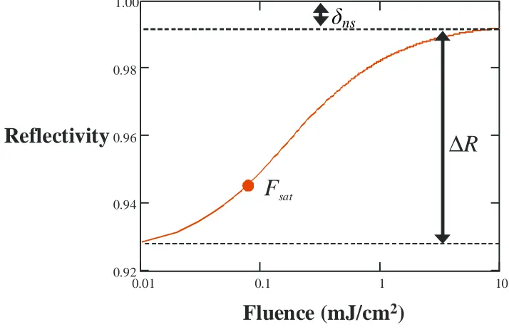
0.01 0.1 1 10
0.92 0.94 0.96 0.98
RGaussTPA402
( )
FpFp
Fluence (mJ/cm
2)
1.00
L
ns? R
F
satReflectivity
∆
∆
R
F
satFig. 1.10. Typical fluence-dependent reflectivity curve illustrating saturation fluence, modulation depth
and non-saturable losses of the device.
SESAMs can be designed to provide various amounts of absorption and to be
saturated at different levels of incident fluence. SESAMs are therefore generally
described by some key parameters which are now defined. The modulation depth, ∆R,
is the amount of saturable absorption present, or the change in reflectivity of the
device experienced as a result of saturation. The linear reflectivity, Rlin, describes the
reflectivity provided at low light levels under no saturation of the absorber layers.
Ideally Rlin and ∆R would add up to 1 as the SESAM would provide 100 % reflectivity
under saturation. However, due to scattering and some non-saturable absorption in the
device, there are always some unwanted losses and these are known as the
non-saturable losses, δns. The saturation fluence, Fsat, is defined by the fluence required to
change the reflectivity by 1/e of its modulation depth. Other characteristics of the
device are the recovery time, τrec, which is the time taken for the absorption to recover
fluence dependant reflectivity curve is shown. Although the SESAM is here described
within the context of mode locking, a SESAM is also often employed as the saturable
absorber in Q-switching where greater modulation depths are typically used.
1.6 Waveguide Theory
A waveguide is a dielectric structure which confines light, allowing light to travel
long distances without diverging, as might otherwise be expected due to diffraction.
Guiding is achieved by using a structure consisting of a high refractive index core
region surrounded by a region or regions of lower refractive index/indices which is
known as the cladding. Light propagates along the core region. The refractive index
profile can gradually change throughout the media, or can be a step-like function. In
the following explanation a step-like function is considered for simplicity. For a
refractive index profile which varies in only one dimension, x, a planar waveguide is
formed, which confines the light in x while allowing the light to diffract along y as the
beam propagates along z. A channel waveguide is formed when the refractive index
varies in two dimensions, x and y, confining the light in these two dimensions with
propagation occurring along the third dimension, z. These two possibilities are
illustrated in fig. 1.11.
Fig. 1.11. Planar and channel waveguides, where light is confined in 1 or 2 dimensions.
In the following explanation the planar waveguide, being the simplest case, is
considered using ray optics. The channel waveguide is an extension of this to include
a further dimension. In-depth considerations of waveguide theory can be found in a
variety of textbooks [106, 107] where explanations using both ray optics and
Maxwell’s equations can be found.
n
1n
1n
2n
3n
2> n
1,3It is necessary to start by recalling that the refractive index, n, of a material is the ratio
of the phase velocity, c, of light in a vacuum to the phase velocity of the light in the
material, υp:
p
c n
υ
= Eq. 1.3
Also recall that for a ray incident on a boundary at angle θi, part of this ray is reflected
at θr (where θr = θi) and part of this ray is refracted at angle θt, where this angle can be
determined from Snell’s law:
sin sin
i i t t
n
θ
=nθ
Eq. 1.4where i and t denote the incidence and transmission sides of a boundary respectively
as illustrated in fig. 1.12.
θ
iθ
rθt
n
in
tFig. 1.12. Ray diagram illustrating the reflection and transmission which occur when light is incident
on a boundary between two media of different refractive indices, where ni > nt.
From Snell’s law, Eq. 1.4, it is apparent that at certain values of θi, defined as those
greater than the critical angle, θc, no solution for θt can be found, provided ni > nt.
Instead, all the light is reflected in a condition known as total internal reflection. In the
case of a second boundary, as illustrated in fig. 1.13, reflection occurs at both
boundaries. This is the basic principle of optical guiding, and explains, using ray
optics, how light is able to propagate over large distances through a core of relatively
high refractive index. A more involved derivation can be found by considering
same result but with an additional feature: this is that the field of the propagating
beam extends slightly beyond the boundary in what is known as the evanescent field.
This evanescent field decays exponentially as it permeates the boundary. As a result
of this, the reflected wave experiences a small phase shift upon reflection, known as
the Goos-Hänchen shift [108].
n
2n
1 [image:41.595.151.446.419.636.2]n
3Fig. 1.13. If θ2 is greater than the critical angle, and n2 is greater than n1,3, then total internal reflection
occurs at both boundaries allowing optical guiding.
From this simple treatment it may seem that guiding can occur for a continuum of
angles, θ, so long as θ> θc and ni > nt. However, there is a third condition which must
be met and this is known as the standing wave condition.
n
2
n
1
n
3
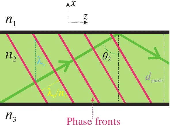
Phase fronts
λ
xλ
0/n
2x
z
d
guideFig. 1.14. Illustration of wavelength of the x component of the electric field, which is used to derive the
waveguide standing wave condition.
The ray illustrated in fig. 1.14 has an electric field which has a component in the x and
z directions. If we consider the component along the x direction we see that this
electric field component travels both along +x and –x, due to the reflection at the
θ
2boundary. This electric field component has a wavelength, λx, which from basic
trigonometry is given by:
0
cos x
i i
n
λ
λ
θ
= Eq. 1.5
In order for the propagating ray to be contained in the x direction it therefore follows
that the wavelength, λx, of the +x and –x electric field components must interfere to
form a standing wave. If this were not the case a travelling wave would be formed
which would propagate in the x direction, and thus the power would be lost from
within the core region. Thus, upon a round trip of the field about the x-direction,
2dguide, there must be an integral number, m, of 2π phase shifts. The round-trip phase
shift caused by the number of wavelengths of the x-component of the electric field
minus the Goos-Hänchen phase shift, φ1 and φ2, for each reflection must therefore
equal an integral number of 2π:
1 2
2
2 2
guide
x
d
m
π ϕ ϕ
π
λ
− − = Eq. 1.6Combining this with Eq. 1.5 we find
2 2
1 2
0
4 cos
2 guide
d n
m
π
θ
ϕ ϕ
π
λ
− − = Eq. 1.7or
1 2
0 2cos 2
2 2
guide
k d n
θ
−ϕ ϕ
− =mπ
Eq. 1.8This is the standing wave condition where m is the mode number. Three conditions
which must be met in order to attain guiding have now been presented, and it is found
that, provided n2 > n1,3 and θc > θ2, certain discrete propagation angles, or modes, can
Eq. 1.9 for a transverse electric (TE) mode or Eq. 1.10 for a transverse magnetic (TM)
mode.
2 2 2
1 2 2 1
2 2
sin tan
2 cos
TE n n
n
ϕ
θ
θ
−= Eq. 1.9
2 2 2
1 2 2 2 1
2
1 2
sin tan
2 cos
TM n n n
n
ϕ
θ
θ
−= Eq. 1.10
When characterising optical waveguides some normalised parameters are often used,
and so these will now be defined.
The normalised frequency parameter, V, is given by:
2 2
0 guide 2 1
V =k d n −n Eq. 1.11
An effective index of the guide, neff, is defined as the ratio of the z component of k, kz,
to k, thus:
2 2 0 sin z eff k n n k
θ
= = Eq. 1.12
We can then define a normalised guide index, b:
(
)
(
)
2 2 1 2 2 2 1 eff n n b n n − =− Eq. 1.13
Finally an asymmetry parameter, a, for the general case where n1 ≠ n3 is introduced:
2 2 3 1 2 2 2 3 TE n n a n n − =
2 2
2 1
TM TE
n
a a
n
=
Eq. 1.15
where TE and TM represent Transverse Electric and Transverse Magnetic modes
respectively.
These can be substituted into Eq. 1.8 to provide a generalised standing wave condition
[109]:
1 1
1 tan tan
1 1
b b a
V b m
b b
π
− − + − = + +
− −
Eq. 1.16
A numerical simulation of Eq. 1.16 gives rise to b versus V plots, which allows neff to
be calculated for a given normalised frequency, V, and mode, m. When neff tends to n3
then b tends to zero, and in practical terms this means the mode is very weakly
confined to the core and thus experiences large exponential decay into the cladding.
For b < 0 no real solution is found, and guiding does not occur. By setting b = 0 in
Eq. 1.16 we can determine the normalised cut-off frequency, Vm, which can support
the m-th order mode. From this we can find the minimum thickness, dguide, able to
support a given wavelength, λ, or the maximum wavelength, λ, which can be
supported for a given core thickness. As b tends to 1, neff tends to n2, and so tight
confinement is achieved with a very small evanescent field.
An interesting point to note is that for the special case when n1 = n3 then the
fundamental mode (m = 0) is not cut-off, and all wavelengths can be guided along
such a symmetric waveguide, no matter how thin the core.
The above derivation is for the simple case of a planar waveguide. Channel
waveguides are similar, although slightly more complex, and so the mode cut-off
conditions for channel waveguides will only briefly be presented here. As before, in
Eq. 1.11:
2 2
2


![Fig. 1.5. Stark energy levels for Yb:KGdW and Yb:KYW [90]. These values correspond to a temperature of 77 K](https://thumb-us.123doks.com/thumbv2/123dok_us/8697450.380912/31.595.99.491.468.720/fig-stark-energy-levels-kgdw-values-correspond-temperature.webp)