Simulation & Analysis of Power Convertors
using Software Tools – A Review
M. Mahendran1, A.S.Viswanathan2
1, 2
Department of Electrical & Electronics Engineering Sri Chandrasekharendra Saraswathi Viswa Mahavidhyalaya, Tamil Nadu, India
Globally the teaching process has changed because of the incomparable growth in the computing technologies and tools. The Design and development Industry requires the students with the enhanced knowledge of software tools. Hence it is mandatory for the educational institutions to equip students with additional software knowledge. Also the use of software’s in teaching learning process helps the students with better understanding of complex concepts easily, learn the design concepts and using multimedia concepts along with technical software’s helps the students to visualise the operation of electrical and electronics circuits. Some of the software’s we use are Matlab, Simulink, Pspice, Psim, MiPower, Magnet, VI tools etc... One such tool we use to teach complex power electronics circuits is PSIM. This article explains the operation of Fully controlled rectifier a simple power converter circuits using PSIM.
Key words: Software, PSIM, Controlled converter, R Load, L Load, Back emf Loads.
I. INTRODUCTION
Power Electronics is a subject which is primarily interdisciplinary in nature, comprising of Power, Electronics and Control, which are three major technological areas and finds its vast applications in Industrial drives control from process industries to automotives, computers to home appliances. Hence forth the importance of power electronics and control has matured vastly. Before the development of Power electronic components, its design is of primary importance relating to the applications. Software based computer simulation can help the design engineers to create a error free design before it goes to the development stage. Hence forth the teaching the simulation concepts to the students in the Universities are of vital for them to find employment in those fields. We use simulation software such as Matlab, Simulink, Pspice, Psim, MiPower, Magnet and Labview as software tools to teach various concepts in electrical engineering to our students. Most important tool we use to teach Power electronics Concepts is PSIM from PowerSim Tech Corporation, which the students finds as a flexible tool to learn. The advantage of this tool is the ease with which we can change the variables to learn the behavior of the system. In this article we have simulated the Full bridge rectifier circuit under various load conditions to estimate its performance parameters.
II. POWER CONVERTORS
Power converters are a type of semiconductor based conversion devices which is used to convert the power from of AC to DC , AC to AC, DC to AC , DC to DC. These topologies are used to modify the characteristics of electrical power supply to load components meeting the requirements of a particular application. In these convertor circuits devices, SCR, MOSFET, IGBT or BJT can be used as semiconductor devices. In our experimentation we used SCR as the power device. The SCR is triggered at a particular firing angle α in both the positive and negative half cycle to control the output voltage.
III. AC – DC FULL BRIDGE RECTIFIER CIRCUIT
The single phase fully controlled rectifier consists of 4 SCRS connected in the bridge form. The experimentation is carried out with R, RL and RLE (Motor) Load. Here for the purpose of explanation, rectifier with resistive load is given. The simulation is carried out for all the three types of load.
Fig. 1 : Single Phase Full Bridge Rectifier with R – Load
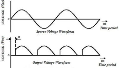
Fig. 2 : Single Phase Full Bridge Rectifier – R Load– Supply and Output Voltage Waveform
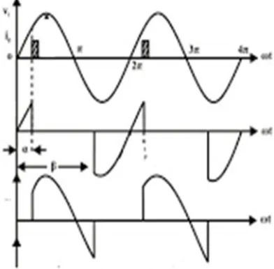
A. During Positive half Cycle
The supply is in positive half cycle of sinusoidal input;
At a time instant of t = 0. Thyristors T1 & T4 are in ON period due to forward biasing and T2 and T3 are in off mode due to reverse bias. T1 and T4 won’t conduct.
At a time period t = α, firing or gate signal is given to the Gate terminal of the SCR. At this time junction breakdown happens and
the thyristors T1 and T4 conducts
Vo = Vac
=
=
At a time period t = π, the supply reaches natural zero and hence T1 and T4 turns reverse biased and hence don’t conduct
B. During Negative Half Cycle
The Supply is in the negative half cycle of sinusoidal input;
At a time period t = π. Thyristors T2 & T3 are ON due to forward biasing and T1 and T4 are in off mode due to reverse bias. T2
and T3 won’t conduct.
At a time period t = π+α, firing or gate signal is given to the Gate terminal of the SCRs T2 and T3. At this time junction breakdown happens and the thyristors T2 and T3 conducts
Vo = Vac
At a time period t = 2π, the supply reaches natural zero and hence T3 and T2 turns reverse biased and in off mode and the cycle
[image:2.612.216.407.253.363.2]Fig. 3 : Single Phase Full Bridge Rectifier with RL – Load
Fig. 4: Single Phase Full Bridge Rectifier – RL Load– Supply and Output Voltage Waveform
[image:3.612.182.418.546.690.2]Fig. 6: Single Phase Full Bridge Rectifier – RLE Load– Supply and Output Voltage Waveform
IV. SIMULATION
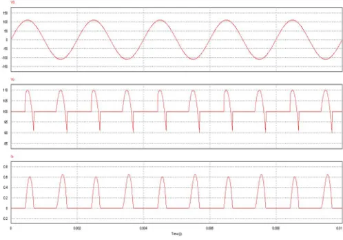
[image:4.612.238.386.81.240.2]The simulation is carried out in PSIM software. PSIM is a electronic simulation software exclusively designed for power electronics, motor drives and its control strategies in both open loop and closed loop. With high speed simulation and user friendly GUI, PSIM provides a powerful simulation package for power electronics studies. Fig. 7 - 12 shows SCR based full bridge convertor circuit diagram for all the three loads in PSIM and its output waveforms. The design Parameters taken are supply voltage Vs as 100V, For R Load circuit, Resistance is 1kohm, for RL Load Inductance L is taken as 1m Henry and for RLE Load the Emf is taken as 100 V. The SCR switching frequency is 1kHz. Single phase Full controlled R load:
Fig. 7: Circuit Diagram of R -Load Fig. 8. Waveforms for R - Load
Single phase Full controlled RL load:
[image:4.612.75.252.390.503.2] [image:4.612.335.512.395.508.2]Fig. 10: Waveforms for R - Load
[image:5.612.36.537.498.685.2]Single phase Full controlled RLE load:
Fig. 11: Circuit Diagram of RL –Load Fig. 11: Circuit Diagram of RL -Load
After simulation, the parameters are measured and noted. The parameters calculated are given below in the table with their values. Performance
Parameter R load RL load RLE load
Avg. load voltage 193.21 V 179.33 V 179.33 V
Avg. load current 0.19 A .18 A 0.079 A
RMS. load voltage 226.79 V 229.5 V 230.2 V
RMS .load current 0.23 A .22 A 0.13 A
Input P.F .98 .954 0.999
Efficiency 70.37 63.93 47.38
Form Factor 1.174 1.279 1.283
Ripple Factor 0.61 0.797 0.804
Pdc 36.71 W 32.28 W 14.167 W