STUDY OF OXIDATION BEHAVIOR OF LEAD THIN FILMS BY THERMAL EVAPORATION METHOD
Alfind Paul Frit Arulraj, Deepalakshmi Kanagar
Department of Physics, V.H.N.S.N College, Virudhunagar, Tamilnadu,
ARTICLE INFO ABSTRACT
The lead thin films were deposited onto amorphous glass substrate using
deposition technique by varying annealing time to study its oxidation behaviour. The XRD pattern clearly exhibited the phase changes in accordance with the annealing time and reaches the menopause of PbO at a maximum annealing time
films were ascribed from SEM micrograms. The change in surface morphology or topography with the function of oxidation time was observed from amplitude and functional parameters. The optical UV-Vis
the rise of annealing time. The functional groups were analysed by using FT
Copyright © 2014 Alfind Paul Frit Arulraj et al. This is an open access ar
permitsunrestricted use, distribution, and reproduction in any medium, provided the original work is properly cited.
INTRODUCTION
Over the last few decades, research interest in the study of nanomaterials and their applications has been increasing, since these materials often demonstrate very different properties at the nanoscale level as compared to those at the macro level, such as new optical, magnetic, and electronic characteristics
(Rosenqvist et al., 2003; Cha et al., 2008;
2009; Baker et al., 2002). Furthermore, nanomaterials with
high aspect-ratio structures and large surface areas offer exciting research possibilities because of such novel physical or chemical properties. As a result, the synthesis and characterization of one and two-dimensional metal oxide nanostructures have attracted considerable attention among the researchers. The different phases (α, β) and mixture of lead
oxide films such as PbO, Pb2O, PbO2, Pb2
(IV-VI group) semiconductor materials narrow band gap
(1.28eV–2.80eV) (Droessler et al., 2012)
useful in photovoltaic materials. A number of theoretical and experimental studies have shown an interesting optical and electronic property of lead oxide and suggesting it to be a very useful photovoltaic material with strong absorption c sections, high carrier mobility and conductivity
1966). The nature of the band gap is suitable for photovoltaic materials design, however information on lead
somewhat limited and at times contradictory requiring further
study (Sharon et al., 1998; Thangaraju, 2000
Minoura, 1994). However, few studies have been conducted on the fabrication of lead oxide by vacuum thermal evaporation
*Corresponding author: Jeyakumaran Natarajan,
Department of Physics, V.H.N.S.N College, Virudhunagar, Tamilnadu, India
ISSN: 0975-833X
Vol. 6, Issue, 11, pp.101
Article History:
Received 25th August, 2014
Received in revised form 23rd September, 2014
Accepted 17th October, 2014
Published online 30th November,2014
Key words:
Lead oxide thin films, X-ray diffraction, SEM, AFM, UV-Vis-NIR spectroscopy.
RESEARCH ARTICLE
STUDY OF OXIDATION BEHAVIOR OF LEAD THIN FILMS BY THERMAL EVAPORATION METHOD
Alfind Paul Frit Arulraj, Deepalakshmi Kanagarajan, Prithivikumaran Natarajan and
*Jeyakumaran Natarajan
Department of Physics, V.H.N.S.N College, Virudhunagar, Tamilnadu,
ABSTRACT
The lead thin films were deposited onto amorphous glass substrate using
deposition technique by varying annealing time to study its oxidation behaviour. The XRD pattern clearly exhibited the phase changes in accordance with the annealing time and reaches the menopause of PbO at a maximum annealing time. The surface morphology, particle size and uniformity of the films were ascribed from SEM micrograms. The change in surface morphology or topography with the function of oxidation time was observed from amplitude and functional parameters. The optical Vis spectra showed that the directly allowed transitions band gap values were decreased due to the rise of annealing time. The functional groups were analysed by using FT
is an open access article distributed under the Creative Commons Att unrestricted use, distribution, and reproduction in any medium, provided the original work is properly cited.
Over the last few decades, research interest in the study of nanomaterials and their applications has been increasing, since these materials often demonstrate very different properties at the nanoscale level as compared to those at the macro level, new optical, magnetic, and electronic characteristics
; Chaudhry et al.,
. Furthermore, nanomaterials with large surface areas offer ibilities because of such novel physical or chemical properties. As a result, the synthesis and dimensional metal oxide have attracted considerable attention among the and mixture of lead
2O3 and Pb3O4 are
VI group) semiconductor materials narrow band gap which are found useful in photovoltaic materials. A number of theoretical and studies have shown an interesting optical and electronic property of lead oxide and suggesting it to be a very useful photovoltaic material with strong absorption cross sections, high carrier mobility and conductivity (Schottmiller, . The nature of the band gap is suitable for photovoltaic materials design, however information on lead oxides is contradictory requiring further 2000; Veluchamy and However, few studies have been conducted on the fabrication of lead oxide by vacuum thermal evaporation
Department of Physics, V.H.N.S.N College, Virudhunagar, Tamilnadu, India
because of the lack of practical preparation methods for such
materials (Droessler et al., 2012
of the most widely used techniques of physical vapor deposition (PVD). The deposited coatings or films by this technique are usually have a thickness in the range of angstroms to microns and are composed of a single material or layers of multiple materials. The coating materials can be either molecules, including nitrides and oxides, or pure atomic elements such as both metals and non
system design allows to adjust a number of parameters to obtain desired results for variables such as grain structure, uniformity, thickness, stress, adhesion strength, optical and electrical properties.
In the present study, a systematic investigation of lead thin films, oxidized at different annealing time, shows a remarkabl difference in structural, surface morphological and optical properties.
MATERIALS AND METHODS
Thin films of Lead (Pb) were deposited onto a glass substrate by vacuum thermal evaporation method. The lead thin films were obtained by evaporating commercia
powder (99.9% Aldrich) from an electrically heated molybdenum boat at about 4 x 10
substrate was heated using a substrate heater at 373K. The deposited Pb films were oxidized at 543 K by varying annealing time. The important step before the deposition of films is the careful cleaning of the substrates. As the cleanliness of the substrate has a direct bearing on the
International Journal of Current Research Vol. 6, Issue, 11, pp.10140-10146, November,2014
STUDY OF OXIDATION BEHAVIOR OF LEAD THIN FILMS BY THERMAL EVAPORATION METHOD
ajan, Prithivikumaran Natarajan and
Department of Physics, V.H.N.S.N College, Virudhunagar, Tamilnadu, India
The lead thin films were deposited onto amorphous glass substrate using a vacuum thermal deposition technique by varying annealing time to study its oxidation behaviour. The XRD pattern clearly exhibited the phase changes in accordance with the annealing time and reaches the menopause rface morphology, particle size and uniformity of the films were ascribed from SEM micrograms. The change in surface morphology or topography with the function of oxidation time was observed from amplitude and functional parameters. The optical tra showed that the directly allowed transitions band gap values were decreased due to the rise of annealing time. The functional groups were analysed by using FT-IR techniques.
ticle distributed under the Creative Commons Attribution License, which
because of the lack of practical preparation methods for such 2012). Thermal evaporation is one of the most widely used techniques of physical vapor deposition (PVD). The deposited coatings or films by this technique are usually have a thickness in the range of angstroms to microns and are composed of a single material or ayers of multiple materials. The coating materials can be either molecules, including nitrides and oxides, or pure atomic elements such as both metals and non-metals. The evaporation system design allows to adjust a number of parameters to esults for variables such as grain structure, uniformity, thickness, stress, adhesion strength, optical and
In the present study, a systematic investigation of lead thin films, oxidized at different annealing time, shows a remarkable difference in structural, surface morphological and optical
MATERIALS AND METHODS
Thin films of Lead (Pb) were deposited onto a glass substrate by vacuum thermal evaporation method. The lead thin films were obtained by evaporating commercial high purity lead (Pb) powder (99.9% Aldrich) from an electrically heated
molybdenum boat at about 4 x 10⁻⁵Torr. Initially the glass
substrate was heated using a substrate heater at 373K. The deposited Pb films were oxidized at 543 K by varying The important step before the deposition of films is the careful cleaning of the substrates. As the cleanliness of the substrate has a direct bearing on the
adherence of the film, the following procedure was adopted for cleaning the substrates. The slides were washed with liquid detergent and then boiled in concentrated chromic acid (0.5 M) for 2 hours. After which, the slides were kept in the same solution for further 48 hours. The substrates were then washed with double distilled water, and then cleaned by ultra-sonication and de-ionized water. Finally, the substrates were cleaned using acetone (AR grade).
Fig. 1. Schematic diagram of thermal evaporation
Fig 1. shows the schematic diagram of thermal evaporation technique. The deposited Pb films were annealed at 543K 30 min, 60 min, 120 min, and 180 min and then characterized.
Characterizations
The X-Ray Diffraction (XRD) patterns were obtained for the prepared lead oxide thin films with X’Pert PRO Diffractometer using CuKα1 radiation (λ=1.54060 Å) with operating voltage 15 KV and a current of 30 mA. Scanning electron micrographs were obtained with HITACHI S-3000 N. Topography or surface morphology of lead oxide thin films was characterized using a Park Systems XE70 instrument, and it was conducted in the ambient atmosphere in non-contact mode. The scan resolution is 64 pixels x 64 pixels, set point 0.7µm and scan rate 0.5 Hz.Optical transmission spectra were taken in the wavelength range 300 – 800 nm using Schimadzu UV-Visible
1800 double beam spectrophotometer. The infrared
transmittance spectra of the prepared samples were measured at
room temperature in the range 1200–400 cm−1 using a
recording PerkinElmer FTIR spectrophotometer. Thickness of the films was obtained by Stylus Profilometer Mitutoyo Surftest SJ – 301.
RESULTS AND DISCUSSION
X-Ray diffraction
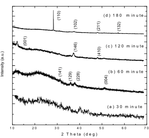
The X-Ray Diffraction (XRD) pattern of lead oxide thin films, compounds with the function of annealing time was shown in Fig. 2.
1 0 2 0 3 0 4 0 5 0 6 0 7 0
2 T h e t a ( d e g )
( a ) 3 0 m i n u t e
(004)
(1
29)
(2
28)
(1
4
1)
Intensit
y
(a.
u
.)
( b ) 6 0 m i n u t e
(4
10)
(1
4
6)
(1
32)
( c ) 1 2 0 m i n u t e ( d ) 1 8 0 m i n u t e
(0
01)
(2
11)
(1
02)
(11
0)
Figure 2. X-ray diffraction pattern of lead films oxidized at 543K for different annealing time
The lower annealing time respective thin film has no diffraction peaks which mean that the films is in amorphous nature. The diffraction patterns corresponding for 60 min and
120 min reveal that mixed compounds of lead oxides (Pb3O4
and Pb2O3). The monophasic lead oxide thin films was only
[image:2.595.38.292.167.350.2]achieved in 180 min. The mixed compounds of lead and oxide in the thin films at lower annealing times react with each other and form the mono phase of lead oxide at a higher annealing time of 180 min. Fig 2. (d) shows four diffraction peaks along the miller planes (110), (102), (211) and (132) at 2 values of 31.8˚, 42.9˚, 55.23˚ and 66.48˚. These diffraction peaks were matched with standard JCPDS data of lead oxide.
Table 1. Comparisons of the results from XRD analysis of the Lead oxide thin films
Annealing time (min)
Position (2 ) (deg) Standard Observed
JCPDS Card No
Stoichi ometry
System
30 - - - - -
60 35.46 35.44 761831 Pb2O3.33 Monoclinic
41.06 41.09 761831 Pb2O3.33 Monoclinic
43.04 43.10 761831 Pb2O3.33 Monoclinic
56.03 56.01 761831 Pb2O3.33 Monoclinic
120 12.55 12.68 230331 Pb2O3 Monoclinic
42.44 42.42 730532 Pb3O4 Tetragonal
55.36 55.38 710562 Pb3O4 Orthorhombic
180 31.80 31.83 851739 PbO Tetragonal
42.85 42.96 850711 PbO Tetragonal
55.15 55.23 850711 PbO Tetragonal
66.30 66.48 851289 PbO Tetragonal
The crystallite sizes were estimated by applying Debye Scherrer’s formula (Cullity, 1956).
D = 0.94λ/βcosθ ... (1)
[image:2.595.300.561.501.629.2]The dislocation density δ, which represents the amount of defects in the film, was determined from the formula (Beltran
et al., 2003),
δ = 1/D2 ...(2)
The micro strain (ε) was calculated by the formula (Bedir
et al., 2005),
ε = βcosθ/4 ...(3)
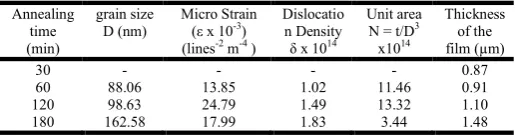
The thicknesses (t) of the as-prepared thin films are increased with increasing annealing time, which means that the rise in particle size is due to the merging of smaller crystals (Peter 1979).
The number of crystallites per unit area (N) of the films is
estimated using the relation (Ning et al., 2006).
= / ………...(4)
[image:3.595.333.532.51.199.2] [image:3.595.337.531.231.374.2]The calculated values of crystallite size, micro strain, dislocation density and unit area crystallite are given in Table 1.2.
Table 1.2. Grain size, Micro strain and Dislocation density of lead oxide thin films
Annealing time (min)
grain size D (nm)
Micro Strain
(ε x 10-3)
(lines-2 m-4 )
Dislocatio n Density
δ x 1014
Unit area
N = t/D3
x1014
Thickness of the film (µm)
30 - - - - 0.87
60 88.06 13.85 1.02 11.46 0.91
120 98.63 24.79 1.49 13.32 1.10
180 162.58 17.99 1.83 3.44 1.48
3. Scanning Electron Microscopy (SEM)
The Scanning electron microscopy (SEM) image of lead oxide thin films as a function of annealing time was shown in Fig. 3.1 – 3.4. The SEM image clearly shows that the particle size and crystallinity increase with increase in annealing time. The thin film annealed for 180 min shows the higher crystalline nature.
Figure 3.1. SEM images of lead films annealed at 543K, for 30 min
[image:3.595.34.292.399.467.2]Figure 3.2. SEM images of lead films annealed at 543K, for 60 min
[image:3.595.334.530.417.564.2]Figure 3.3. SEM images of lead films annealed at 543K, for 120 min
Figure 3.4. SEM images of lead films annealed at 543K, for 180 min
[image:3.595.62.268.579.734.2]Atomic Force Microscopy (AFM)
The van der Waals forces (FvdW) are interactive force acting between tip and sample was estimated by using the following relation,
FvdW = HR/6d2 ……….(5)
H is the Hamaker constant and is in the order of 10−19 J, and R
[image:4.595.321.551.51.354.2]is the tip radius, and d is the spacing between tip and sample. The van der Waals forces are significantly affected by the medium in the gap between tip and sample.
Figure 4.1. AFM 2-D & 3-D images of lead films annealed at 543K for 30 min
[image:4.595.311.552.53.713.2]Figure 4.2. AFM 2-D & 3-D images of lead films annealed at 543K for 60 min
Figure 4.3. AFM 2-D & 3-D images of lead films annealed at 543K for 120 min
[image:4.595.75.250.184.442.2] [image:4.595.74.253.478.735.2]The results of an AFM surface roughness analysis of the lead oxide thin films over a scanning area, 2.5 µm x 2.5 µm are shown in Fig 4. Fig 4.1 – 4.4 shows the 2-dimensional surfaces of lead oxide thin films, and three-dimensional topography of lead oxide films, where roughness are seen with well-defined grains. The roughness gives an impressive insight of the excellent capability of the method to measure surface topography. To study the changes in roughness of the film, it is very important that the area analysed should remain well adhered to the substrate. It is also important that the area chosen to be the same for all measurements. In order to quantitatively describe the surface morphology, Scaling theory (Family and Vicsek, 1991; Barabasi and Stanley, 1995) was used to analyse the quantitative information on the surface
morphology of AFM data. The amplitude parameters like Ra,
Rq and Rmax are used to evaluate the surface morphological
properties of the thin films while functional parameters (Rskw,
Rkur) are used to evaluate the surface topography. In this work
[image:5.595.313.544.87.278.2]both amplitude and functional parameters are calculated as a function of annealing time and are given in Table 2.
Table 2. Analysis of the AFM profile of lead oxide thin films
Annealing time (min)
Rp-v
(nm) (Rq)
(nm) (Ra)
(nm)
Rskw Rkur Rz (nm)
30 50.87 11.34 9.23 0.38 2.73 31.30
60 113.15 31.36 27.00 0.24 1.85 77.05
120 41.58 8.08 6.49 -0.78 3.64 25.76
180 30.83 5.75 4.17 -1.40 5.60 21.65
The Skewness and kurtosis are used to measure symmetry and
peaks of the surface (Family et al., Barabasi et al., 1991). The
Skewness (Rskw) of the lead oxide films is close to 0 and
kurtosis (Rkur) lies in the range of 1.8 to 5.6. It indicates that,
the surfaces exhibited an asymmetrical distribution of grain and irregular shaped peaks and valleys. The AFM results are in good agreement with the SEM and XRD results.
Optical properties
300 400 500 600 700 800
0.0 0.4 0.8 1.2 1.6 2.0 2.4 2.8 3.2 3.6 4.0
Absorban
ce
Wavelength (nm)
(d) (a) (b)
[image:5.595.31.295.317.379.2](c) a) 30 minute b) 60 minute c) 120 minute d) 180 minute
Figure 5.1. Plot of optical absorption versus wavelength for lead oxide films
Fig. 5.1 shows the variation of optical absorption A with wavelength λ. All the films show lower absorption in the
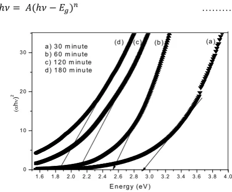
visible wavelength region. The nature of the transition (direct or indirect) was determined by the relation.
ℎ = (ℎ − ) ………..(6)
1 .6 1 .8 2 .0 2 .2 2 .4 2 .6 2 .8 3 .0 3 .2 3 .4 3 .6 3 .8 4 .0 0
1 0 2 0 3 0
a ) 3 0 m in u te b ) 6 0 m in u te c ) 1 2 0 m in u te d ) 1 8 0 m in u te
h
)
2
E n e rg y (e V )
(a ) (b )
[image:5.595.316.547.492.681.2](d ) (c )
Figure 5.2. Plot of (αhυ)2 versus Energy for lead oxide films
From the transmittance data and the Tauc’s (Tauc, 1974)
relation, allowed direct transitions ((αhυ)2) versus incident
photon energy (E), plots were obtained. The allowed direct transitions (n = ½) curve is shown in Fig. 5.2. The band gap
energy Egwas determined by extrapolating the tangent line
portion to the x-axis for zero absorption coefficients α, and the
values of Eg are in a good agreement with other reports
(Droessler et al., 2012). The calculated optical energy band gap
was in between 2.92eV and 1.84eV.
The extinction coefficient (or) total attenuation coefficient
kwas employed from the relation (Mahmoud et al., 2009).
k = αλ/4π …………(7)
300 350 400 450 500 550 600 650 700 750 800
0 20 40 60 80 100 120
(d) (c) (b)
Ex
tinct
ion c
oe
ff
ic
ient
Wavelength (nm) a) 30 minute b) 60 minute c) 120 minute d) 180 minute
(a)
Figure 5.3. Extinction coefficient versus Wavelength for lead oxide films
[image:5.595.56.274.495.672.2]extinction coefficient k decreases with increasing annealing time. The observed k values decrease in the long wavelength range (Ubale and Kulkarni, 2006). The decrease in k with increasing substrate temperature might be due to the improvement in the crystallinity which leads to minimum imperfection.
Fourier Transform Infrared Spectroscopy (FTIR)
The FTIR spectroscopy is an analytical tool for the characterization of functional group of thin films. The identified possible modes of vibration from the FTIR spectra of lead oxide thin films are shown in Fig 6.
The absorption peak nearly at 460 cm-1 and 658 cm-1 indicates
the presence of symmetric bending vibration modes of Pb-O bonds and asymmetric bending vibration modes of Pb-O-Pb
(Trettenhahn et al., 1993; Bosca et al., 2009). The intensity of
the band at 658 cm-1 in the spectrum shows the increase in
intensity with increasing annealing time and it strongly recommends the development of Pb-O bonds.
400 600 800 1000 1200
a) 30 minute a) 60 minute c) 120 minute
T
rans
mittanc
e
%
Wavelength (nm)
[image:6.595.48.280.315.505.2]d) 180 minute
Figure 6. FT-IR Spectra of lead oxide films
Conclusion
The preparation of nano-structured lead oxide thin films has been done by a vacuum thermal evaporation method. The x-ray diffraction study shows that, when the oxidation time increases,
the observed Pb2O3 peaks shift to PbO peak with sharp
intensity and reach mono phase PbO at 180 min. The surface characterization of these films studied using scanning electron microscopy and atomic force microscopy, which reveals that uniform coating renders spherical structures with lower surface roughness. The optical absorption study revealed that, the lead oxide thin films, have allowed direct transitions. All the observed characteristic absorption peaks of the FTIR spectrum confirmed the presence of PbO. The optical energy band gap varied from 2.92eV to 1.84eV with oxidized time and this optical energy band gap is suitable for photovoltaic materials.
REFERENCES
Baker, M.A., Klose, S., Rebholz, C., Leyland, A., Matthews, A. 2002. Evaluating the microstructure and performance
of nanocomposite PVD TiAlBN., coatings., Surf. Coatings
Technol., 151-152, 338-343.
Barabasi, A.L., Stanley, H.E. 1995. Fractal Concepts in
Surface Growth., Cambridge University, Press,
Cambridge, 19-37.
Bedir, M., Oztas, M., Bakkaloglu, O.F. 2005. Investigations on structural, optical and electrical parameters of spray deposited ZnSe thin films with different substrate
temperature, Euro. Phys. J., 45, 465.
Beltran, A., Andres, J., Longo, E., Leite, E.R. 2003. Thermodynamic argument about SnO[sub 2] nanoribbon
growth, Appl. Phys. Lett., vol. 83, 4, 635.
Bosca, M., Pop, L., Borodi, G., Pascuta, P., and Culea, E. 2009. XRD and FTIR structural investigations of
erbium-doped bismuth-lead-silver glasses and glass ceramics, J.
Alloys Compd., 479, 1-2, 579-582.
Cha, L., Scheu, C., Clemens, H., Chladil, H.F., Dehm, G., Gerling, R., Bartels, A. 2008. Nanometer-scaled lamellar microstructures in Ti-45Al-7.5Nb-(0; 0.5)C alloys and
their influence on hardness., Intermetallics, 16, 7,
868-875.
Chaudhry, B., Ashton, H., Muhamed, A., Yost, M., Bull, S., Frankel, D. 2009. Nanoscale viscoelastic properties of an
aligned collagen scaffold, J. Mater. Sci. Mater. Med., 20,
1, 257-63.
Cullity, B.D. Elements of X-ray Diffraction, 1956, Addison-Wesley Pub. Co.
Droessler, L.M., Assender, H.E., Watt, A.A.R. 2012. Thermally deposited lead oxides for thin film
photovoltaics, Mater. Lett., vol. 71, 51-53.
Family, F., Vicsek, T., Dynamics of Fractal Surfaces., World Scientific, Singapore, 1991, 5-11.
Mahmoud, S.A., Akl, A.A., Al-Shomar, S.M. 2009. Effect of some preparative parameters on optical properties of spray
deposited iridium oxide thin films., Phys. B Condens.
Matter, 404,16, 2151-2158.
Ning, X.J., Li, C.X., Li, C.J., Yang, G.J. 2006. Modification of microstructure and electrical conductivity of plasma-sprayed YSZ deposit through post-densification process.,
Mater. Sci. Eng. A, 428, 1-2, 98-105.
Peter L. M. 1979. The photoelectrochemical properties of
anodic Bi2S3 films., J. Electroanal. Chem. Interfacial
Electrochem, vol. 98, no. 1, pp. 49-58, Apr.
Rosenqvist, J., Axe, K., Sjoberg, S., Persson, P. 2003. Adsorption of dicarboxylates on nano-sized gibbsite particles: effects of ligand structure on bonding
mechanisms., Colloids Surfaces A Physicochem. Eng.
Asp., 220, 1-3, 91-104.
Schottmiller, J.C. 1966. Photoconductivity in Tetragonal and
Orthorhombic Lead Monoxide Layers., J. Appl. Phys., 37,
9, 3505.
Sharon, S.G.M., Lee, Y.S., Whang, C.N. 1998. Effect of platinum on the photoelectrochemical behavior of lead
oxide thin film., J Solid State Electrochem, 2, 6, 386-93.
Thangaraju, P.K.B. 2000. Optical and structural studies on
spray deposited α-PbO thin films., Semicond Sci Technol.,
15,6, 542-545.
Trettenhahn, G.L.J., Nauer, G.E., Neckel, A. 1993. Vibrational spectroscopy on the PbO-PbSO4 system and some related
compounds., Vib. Spectrosc., 5, 1, 85-100.
Ubale, A.U., Kulkarni, D.K. 2006. Studies on size dependent properties of cadmium telluride thin films deposited by using successive ionic layer adsorption and r eaction
method, Indian J. Pure. Appl. Phys., 44, 254-259.
Veluchamy, P., Minoura, H. 1994. Simple electrochemical method for the preparation of a highly oriented and highly
photoactive α-PbO film., Appl. Phys. Lett., 65, 19, 2431.