N A N O E X P R E S S
Open Access
The deviation of growth model for transparent
conductive graphene
Shih-Hao Chan
1, Jia-Wei Chen
1, Hung-Pin Chen
1, Hung-Sen Wei
1, Meng-Chi Li
1,3, Sheng-Hui Chen
1, Cheng-Chung Lee
1and Chien-Cheng Kuo
1,2*Abstract
An approximate growth model was employed to predict the time required to grow a graphene film by chemical vapor deposition (CVD). Monolayer graphene films were synthesized on Cu foil at various hydrogen flow rates from 10 to 50 sccm. The sheet resistance of the graphene film was 310Ω/□and the optical transmittance was 97.7%. The Raman intensity ratio of the G-peak to the 2D peak of the graphene film was as high as ~4 when the hydrogen flow rate was 30 sccm. The fitting curve obtained by the deviation equation of growth model closely matches the data. We believe that under the same conditions and with the same setup, the presented growth model can help manufacturers and academics to predict graphene growth time more accurately.
Keywords:Graphene; Transparent conductive electrode; Chemical vapor deposition
Background
Graphene, comprising two-dimensional monolayer of sp2-bonded carbon atoms, has attracted substantial atten-tion for use in transparent conductive electrodes (TCE), owing to its chemical stability and high optical transmit-tance from the ultraviolet to the infrared regions. Gra-phene as a TCE has a wide range of applications, including in solar cells, solid-state lighting, and detectors, owing to not only its higher optical transmittance but also its more favorable conductance [1-4] than those of traditional trans-parent conductive electrodes, such as indium tin oxide (ITO) and zinc oxide (ZnO) [5]. (Additionally, Further-more, or Moreover), ITO is an expensive material, and it is unstable in chemical solution and cannot be utilized in a hydrogen-containing environment. ZnO-based thin film has also attracted interest for use in TCEs owing to its low cost, non-toxicity, and abundant constituent ele-ments [6]. However, the properties of ZnO-based thin films are not uniform or stable. The several ways to pro-duce graphene include mechanical exfoliation, graphene oxide (GO), and chemical vapor deposition (CVD). Mechanical exfoliation can yield high-quality graphene
from graphite but this method produces graphene over a small area of the order of only a few tens of microme-ters [4]. Graphene oxide can be formed by oxidizing graphite flakes; this method can produce large quantities of graphene whose electrical properties are, however, af-fected by the functional groups and various defects in the graphene [7]. Nevertheless, CVD is a promising method for growing high-quality graphene over a large area using Cu foils. Li et al. were the first to grow graphene over a large area of the order of square centimeters on Cu foil by CVD using methane, and this method has become a stand-ard approach to forming graphene films in recent years [8]. Four-layered graphene exhibits a sheet resistance of about 350Ω/□, which represents a large step toward lower sheet resistance and a large increase in the range of graphene applications [9]. Additionally, various methods have been proposed to optimize the properties of CVD graphene [10-14]. This work develops a simply derived graphene growth model to predict the growth time with various hydrogen flow rates.
Methods
Graphene films were grown by chemical vapor deposition (APCVD) on 25-μm-thick Cu foils (99.8%, Alfa-Aesar, item no. 13382) in a 3-in. quartz tube furnace under at-mospheric pressure. Beforehand, electrochemical pol-ishing (50% H3PO4in deionized water of 100 mL) was * Correspondence:[email protected]
1
Department of Optics and Photonics/Thin Film Technology Center, National Central University, 300 Chung-Da Rd, Chung-Li 32001, Taiwan
2
Graduate Institute of Energy Engineering/Thin Film Technology Center, National Central University, 300 Chung-Da Rd, Chung-Li 32001, Taiwan Full list of author information is available at the end of the article
utilized to smooth out the foil, and a voltage from 2 to 4 V was applied until the Cu foil glowed. Thereafter, the Cu foil was rinsed in a large amount of deionized water with sonication and then blow-dried with nitrogen gas. The Cu foil was placed in the reaction chamber, the Ar and H2(1,000 and 2 sccm, respectively) gases were
in-troduced into the chamber during temperature ramp-up. The Cu foil was annealed at 1,070°C for an hour. Then, 0.3 sccm of methane (purity, 99.99%) was used as a source of carbon to grow the graphene. The H2flow rate was
var-ied from 10 to 50 sccm prior to observation of the morph-ology of the graphene domains and the nucleation density. Following the growth process, the as-grown graphene/Cu foil was removed from the heating zone for rapid cooling. Polymethyl methacrylate (PMMA) was spin-coated on the as-grown graphene/Cu foil as a supporting layer to pre-vent any cracking during the transfer process. The gra-phene grew on both sides of the Cu foil. The gragra-phene at the back of the foil was removed by floating on nitride acid solution (30% in deionized water) for 10 s. The Cu foil was etched away overnight using an ammonium per-sulfate solution (0.1 M) and then rinsed three times in de-ionized water. The PMMA/graphene was placed on the substrate, and the PMMA was then dissolved in hot acet-one bath for 24 h. The residual PMMA was removed by annealing in air at 200°C for an hour and reduced to pris-tine graphene using an H2/Ar (7/20 sccm) mixture. The
[image:2.595.60.540.89.351.2]morphology and the nucleation density of the graphene domain were measured by scanning electron microscopy (SEM); The surface profile of Cu foils were measured by atomic force microscopy (AFM); the sheet resistance was measured using a four-probe stage; the Raman shift of the graphene was measured by Raman spectroscopy using a laser with a wavelength of 532 nm, the laser power at the focused spot was 2 mW, and the numerical aperture value was 0.75 on the sample with an area of 1μm2.
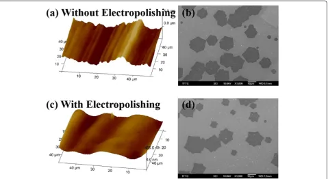
Figure 1Surface profile of Cu foil and SEM images of graphene domains.Surface profile of Cu foil(a)before and(c)after electropolishing. (b)SEM image of morphology of graphene domains(c)before and(d)after electropolishing.
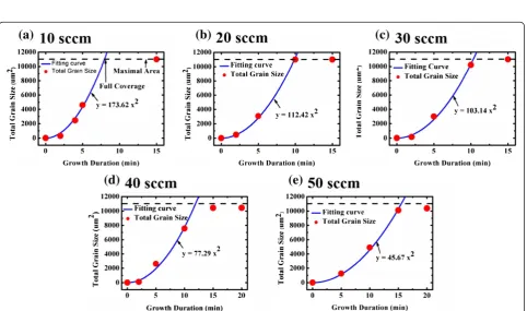
[image:2.595.306.538.545.706.2]Figure 4Growth model of graphene at various hydrogen flow rates and corresponding fitting curves. (a)10,(b)20,(c)30,(d)40, and (e)50 sccm.
Figure 3Results of growth model and SEM image.Results of growth model with growth time of(a)t1and(b)t2.(c)SEM image of
Results and discussion
The number of graphene layers, the shape, and the nu-cleation density were significantly influenced by the sur-face roughness of Cu foil. Figure 1a,c presents AFM images of the reduction of the rolling marks on the Cu foil by electropolishing. The domain density of graphene clearly declined from Figure 1b-d, and the graphene morphology became star-shaped under hydrogen at a 1flow rate of 20 sccm. In the latter experiments, the electropolishing of Cu foils were applied for growing graphene films. To synthesize a larger graphene domain, experiments were conducted in which the hydrogen flow rate was increased from 10 to 50 sccm, and the
[image:4.595.62.538.272.706.2]graphene domain density is calculated, as displayed in Figure 2. A previous investigation revealed that the hydrogen flow rate importantly affects the graphene growth mechanism, owing to the etch effect and its effect on the graphene domain density. The density of graphene nuclei is reduced as the hydrogen flow rate is increased. The hydrogen flow rate also affects the morphology of graphene. In this case, the graphene had a hexagonal shape when the hydrogen flow rate was 30 sccm, as shown in Figure 3c. A growth model to elucidate the rate of graphene domain growth was proposed. If the graphene domain is circular, then this model allows the easy cal-culation of the difference between the graphene domain
sizes at two growth times. Figure 3 displays the deriv-ation of the growth model. Figure 3a,b schematically de-picts the growth of the graphene domains from growth timet1tot2. Figure 3d presents the growth model in de-tail, whereL is the circumference of graphene domain;
Ais the mean area of the grown domains, and the ris the average radius of the domains. Now, an area factor is sought such that
dA¼Ldr ð1Þ
For a carbon deposition rate v, the deposition rate of carbon atoms at one direction is given by,
v¼dr
dt ð2Þ
Combining Equations 1 and 2 yields simultaneous equations,
dA¼Lvdt L¼ð4πAÞ
1 2
(
ð3Þ
Solving Equation 3 yields,
4πA
ð Þ−1
2dA¼vdt ð4Þ
1 2πð4πAÞ
1
2¼vt ð5Þ
A¼πð Þvt 2 ð6Þ
The mean areaAnow becomes
A¼πð Þvt 2¼1 2
d2A dt2 t
2 ð7Þ
The A is a quadratic equation which means the gra-phene domains grown with an acceleration rate on the Cu foil. Equation 7 can be utilized to predict the coverage area of graphene on the Cu foil under various hydrogen flow rates from 10 to 50 sccm, as displayed in Figure 4. The dashed line is the area of the Cu foil (1.1 cm2) and the red spots represent the growth times of graphene that yield the specified area, based on Equation 7. A red spot at the dashed line indicates that the graphene fully cov-ered the Cu foil. Figure 4 reveals that the graphene fully covered the foil when the hydrogen flow rate was 10, 20, or 30. When the hydrogen flow rate exceeded 30 sccm, the graphene did not fully cover the Cu foil because of the etching effect and thermal equilibrium occurs on the edge of graphene domains. Also, a fitting equation is obtained for the growth of graphene with different hydrogen flow rate, which is plotted as the blue curve. Based on the de-veloped growth model, we can adjust any coverage of gra-phene on the Cu foil which closely matches the fitting curve; the growth model predicts the growth rate of gra-phene. As mentioned above, the graphene domain was
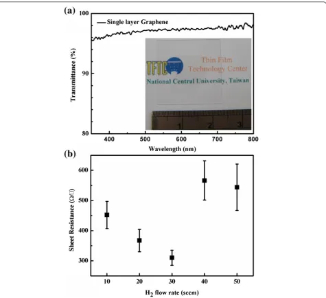
hexagonal when the hydrogen flow rate was 30 sccm. The graphene fully covered the Cu foil both according to the growth model and in the experiment. The graphene was transferred onto a glass substrate to measure its transpar-ency, sheet resistance, and Raman shift. In Figure 5a, the graphene film is placed on the glass substrate with a rela-tively high transmittance of about 97.7% at λ =550 nm. The attenuation coefficient (α =2.3%) was fitted using Beer’s law; the value matches the theoretical value of 2.3% when theλ =550 nm [15]. The graphene films that were synthesized using various hydrogen flow rates were also transferred to the substrate and their sheet resistance was measured, as shown in Figure 5b. The lowest obtained sheet resistance of graphene was 310Ω/□, which was achieved when the hydrogen flow rate was 30 sccm, be-cause the smooth edge of the graphene domain reduced the number of scattering centers which inhibited the car-rier transportation. The sheet resistance increased with the hydrogen flow rate over 30 sccm because the graphene did not fully cover the Cu foil, and because the larger number of pores in the graphene increased the sheet re-sistance. Figure 6 shows the Raman spectrum of graphene film, in which the peaks are typical of a single-layer gra-phene, with a 2D/G ratio of as high as ~4 when the hydrogen flow rate was 30 sccm. The full width at half maximum (FWHM) was 23.5 cm−1, verifying the pres-ence of a single-layer graphene [8].
Conclusions
[image:5.595.306.538.547.714.2]An approximate growth model of the synthesis of gra-phene by APCVD was developed. When the hydrogen flow rate was 30 sccm, the transmittance as a function of wavelength for single-layer graphene reached its max-imum of 97.7% at λ =550 nm. The 2D/G ratio and the FWHM indicated that the graphene comprised a single layer of high quality. The lowest obtained sheet resist-ance of a single layer of graphene was about 310Ω/□.
The results of the experiments closely matched the fitting curve. We believe that, under the same conditions and with the same experimental setup, the proposed growth model can help manufacturers and academics predict the growth time of graphene more accurately.
Competing interests
The authors declare that they have no competing interests.
Authors’contributions
SHC (Chan) designed the study and wrote the paper. JWC, HSW, MCL, and HBC analyzed the data. SHC (Chen), CCL, and CCK are advisors. All authors read and approved the final manuscript.
Acknowledgments
The authors would like to thank the National Science Council of the Republic of China, Taiwan, for financially supporting this research under contract nos. NSC 102-2633-E-008-001, NSC 103-2623-E-008-001-ET, and MOST 103-2221-E-008-101-MY2.
Author details
1Department of Optics and Photonics/Thin Film Technology Center, National Central University, 300 Chung-Da Rd, Chung-Li 32001, Taiwan.2Graduate Institute of Energy Engineering/Thin Film Technology Center, National Central University, 300 Chung-Da Rd, Chung-Li 32001, Taiwan.3Optical Sciences Center/Thin Film Technology Center, National Central University, 300 Chung-Da Rd, Chung-Li 32001, Taiwan.
Received: 1 September 2014 Accepted: 11 October 2014 Published: 20 October 2014
References
1. Wang X, Zhi LJ, Mullen K:Transparent, conductive graphene electrodes for dye-sensitized solar cells.Nano Lett2008,8:323–327.
2. Kim YS, Joo K, Jerng SK, Lee JH, Moon D, Kim J, Yoon E, Chun SH:Direct integration of polycrystalline graphene into light emitting diodes by plasma-assisted metal-catalyst-free synthesis.ACS Nano2014, 8:2230–2236.
3. Chitara B, Krupanidhi SB, Rao CNR:Solution processed reduced graphene oxide ultraviolet detector.Appl Phys Lett2011,99:3.
4. Geim AK, Novoselov KS:The rise of graphene.Nat Mater2007,6:183–191. 5. Wu CC, Wu CI, Sturm JC, Kahn A:Surface modification of indium tin oxide
by plasma treatment: an effective method to improve the efficiency, brightness, and reliability of organic light emitting devices.Appl Phys Lett 1997,70:1348–1350.
6. Kim KH, Park KC, Ma DY:Structural, electrical and optical properties of aluminum doped zinc oxide films prepared by radio frequency magnetron sputtering.J Appl Phys1997,81:7764–7772.
7. Dreyer DR, Park S, Bielawski CW, Ruoff RS:The chemistry of graphene oxide.Chem Soc Rev2010,39:228–240.
8. Li XS, Cai WW, An JH, Kim S, Nah J, Yang DX, Piner R, Velamakanni A, Jung I, Tutuc E, Banerjee SK, Colombo L, Ruoff RS:Large-area synthesis of high-quality and uniform graphene films on copper foils.Science2009, 324:1312–1314.
9. Li XS, Zhu YW, Cai WW, Borysiak M, Han BY, Chen D, Piner RD, Colombo L, Ruoff RS:Transfer of large-area graphene films for high-performance transparent conductive electrodes.Nano Lett2009,9:4359–4363. 10. Hao YF, Bharathi MS, Wang L, Liu YY, Chen H, Nie S, Wang XH, Chou H, Tan C,
Fallahazad B, Ramanarayan H, Magnuson CW, Tutuc E, Yakobson BI, McCarty KF, Zhang YW, Kim P, Hone J, Colombo L, Ruoff RS:The role of surface oxygen in the growth of large single-crystal graphene on copper.Science2013,342:720–723.
11. Kang J, Hwang S, Kim JH, Kim MH, Ryu J, Seo SJ, Hong BH, Kim MK, Choi JB: Efficient transfer of large-area graphene films onto rigid substrates by hot pressing.ACS Nano2012,6:5360–5365.
12. Zhang J, Hu PA, Wang XN, Wang ZL, Liu DQ, Yang B, Cao WW:CVD growth of large area and uniform graphene on tilted copper foil for high performance flexible transparent conductive film.J Mater Chem2012, 22:18283–18290.
13. Vlassiouk I, Regmi M, Fulvio PF, Dai S, Datskos P, Eres G, Smirnov S:Role of hydrogen in chemical vapor deposition growth of large single-crystal graphene.ACS Nano2011,5:6069–6076.
14. Li XS, Magnuson CW, Venugopal A, Tromp RM, Hannon JB, Vogel EM, Colombo L, Ruoff RS:Large-area graphene single crystals grown by low-pressure chemical vapor deposition of methane on copper.J Am Chem Soc2011,133:2816–2819.
15. Nair RR, Blake P, Grigorenko AN, Novoselov KS, Booth TJ, Stauber T, Peres NMR, Geim AK:Fine structure constant defines visual transparency of graphene. Science2008,320:1308–1308.
doi:10.1186/1556-276X-9-581
Cite this article as:Chanet al.:The deviation of growth model for transparent conductive graphene.Nanoscale Research Letters20149:581.
Submit your manuscript to a
journal and benefi t from:
7Convenient online submission 7Rigorous peer review
7Immediate publication on acceptance 7Open access: articles freely available online 7High visibility within the fi eld
7Retaining the copyright to your article