N A N O E X P R E S S
Open Access
Anomalous Inner-Gap Structure in
Transport Characteristics of
Superconducting Junctions with Degraded
Interfaces
E. Zhitlukhina
1, I. Devyatov
2,3, O. Egorov
4, M. Belogolovskii
5*and P. Seidel
6Abstract
Quantitative description of charge transport across tunneling and break-junction devices with novel superconductors encounters some problems not present or not as severe for traditional superconducting materials. In this work, we explain unexpected features in related transport characteristics as an effect of a degraded nanoscaled sheath at the superconductor surface. A model capturing the main aspects of the ballistic charge transport across hybrid superconducting structures with normally conducting nanometer-thick interlayers is proposed. The calculations are based on a scattering formalism taking into account Andreev electron-into-hole (and inverse) reflections at normal metal-superconductor interfaces as well as transmission and backscattering events in insulating barriers between the electrodes. Current-voltage characteristics of such devices exhibit a rich diversity of anomalous (from the viewpoint of the standard theory) features, in particular shift of differential-conductance maxima at gap voltages to lower positions and appearance of well-defined dips instead expected coherence peaks. We compare our results with related experimental data.
Keywords: Superconducting heterostructures, Charge transport, Nanoscale degraded sheath, Anomalous features
Background
The Bardeen-Cooper-Schrieffer (BCS) theory of super-conductivity (S) is based on the assumption that elec-trons in the BCS state are bound into Cooper pairs by a sufficiently weak attractive interaction between them. These pairs are correlated, so that, in order to break a pair, one has to change energies of all other pairs. It means that, unlike in the normal-metal (N) state, there is an energy gap Δ for single-particle excitations. The most complete and convincing evidence for the appear-ance of the energy gap came from the well-known Giaever effect of electron tunneling through N-I-S and S-I-S heterostructures where I stands for a nanometer-thick insulating layer that permits only single-tunneling processes [1]. When an N-I-S trilayer with a
conventionals-wave paring-symmetry superconductor is biased with a voltage V, an electron can be injected into the S side merely if its energy exceeds the gap value Δs. It means that at the environment temperatureT→0, the tunneling currentIacross the junction is vanishing below
VΔ=Δs/e. The nonlinearities in I-Vcurves can be more clearly seen in the quasiparticle differential conductance
dI/dV-versus-Vwhich exhibits coherence peaks atV= ±
VΔfor an N-I-S structure and atV= ± (Δs1+Δs2)/efor an
S1-I-S2trilayer with conventionals-wave superconductors.
This fact can be used as direct measure of the superconducting-order parameter magnitude and its de-pendence on external parameters.
Nowadays, electron tunneling spectroscopy is a well-developed technique aimed to provide extensive informa-tion about energy spectra of conducting electrodes and an insulating interlayer between them [1]. It has been a disap-pointment that tunneling spectroscopy has so far given us no such evidence for novel superconductors. Our work * Correspondence:[email protected]
5Institute for Metal Physics, National Academy of Sciences of Ukraine, 03680
Kyiv, Ukraine
Full list of author information is available at the end of the article
was stimulated by systematic deviations of transport char-acteristics measured for nominally trilayered metal-barrier-metal heterostructures based on novel superconductors from related theoretical predictions for conventional tunnel junctions with a transmission probability D< < 1 [2], as well as for S-c-S devices withD≤1 where c stands for a constriction [3].
The first finding of such kind was revealed for tunnel junctions with some transition metals, especially for Nb-based devices and intensively discussed in the 1970s long before the discovery of high-temperature superconduct-ivity. We mean the so-called knee, a sudden current de-crease in low-temperature I-V characteristics of Nb-based S-I-S junctions at voltages slightly just above a strong increase of the current that was expected to occur at the sum ofVΔvalues for the two superconduct-ing electrodes [4] (see also [5]). Moreover, the current values at very low temperatures and at voltages lower than the sum ofVΔwere considerably larger than theor-etically anticipated for the BCS densities of states [6]. Later, it was shown experimentally that this anomaly may be caused by the presence of a normal conducting layer on the superconducting niobium film [6, 7]. This statement was confirmed theoretically [8] in the framework of the proximity-effect model which treats incoherent single-particle scatterings from a normal layer to a superconducting one within a tunnel-barrier approximation [9]. Below, we discuss the ori-gin of the “knee” phenomenon analyzing ballistic transport in tunneling S-I-S structures where each superconducting electrode is covered by a nanometer-scale degraded sheath.
The next puzzling experimental feature was the so-called peak-dip-hump structure clearly observed in conductance-versus-voltage curves for break junctions based on high-Tc BSCCO samples [10]. In these experi-ments, the peak was attributed to twice the gap magni-tude although the values obtained were systematically lower than those provided by other experimental tech-niques, see Table 3.1 in [10]. But the main problem of the measurements was the presence of a pronounced dip that was revealed in data obtained by STM or ARPES [11] as well. Its derivation has not been clear and, in particular, was believed to represent a physical quantity responsible for pairing in the studied com-pound [12]. It was suggested [13] that the dip appears at the voltage bias (2Δ+Ω)/e where Ω is the energy of some collective excitations that performs a role of glue for paired electrons. The author of ref. [10] studied how the estimated doping level influences the peak and ob-served a large spread of the measured peak positions. Below, we reproduce numerically the “peak-dip-hump” structure and propose our explanation of each of the three elements relating them to the presence of a
degraded layer on the surface of the high-Tc
supercon-ductor. It should be noticed that at early stages of single-electron tunneling experiments, four-layered N-I-n-S heterostructures with a normal (n) interlayer be-tween an ordinary superconductor and the barrier were fabricated and studied. Comparing related data with our simulations, we show that, at least qualitatively, the mea-sured conductance spectra of S-I-n-S samples having the n interlayer for sure do follow our predictions.
The last unusual feature which will be analyzed in the paper relates the inner-gap structure in S-c-S junctions where c stands for a constriction with a transmission probability D≤1. The authors of ref. [14] fabricated two types of symmetric S-c-S trilayers, Al-/InAs-nanowire-Al and Nb-InAs-nanowire-Nb junctions and measured the differential resistance dV/ dI as a function of the voltage bias at various temper-atures. At 0.4 K, the Al-based devices exhibited sub-harmonic gap features at Vn= 2ΔAl/(en); n is an
integer. Due to the theory [3], such features are the manifestation of multiple Andreev reflections within the constriction between two identical superconduc-tors and they should expose themselves as local minima in the resistance-versus-voltage dependence as it was indeed observed for Al-based samples, Fig. 1a in ref. [14]. Similar dV/dI measurements at T< 4 K for a typical Nb-based junction depicted in Fig. 1b in ref. [14] revealed a subharmonic gap structure corresponding to 2ΔNb/e and ΔNb/e, but they were peaks rather than expected dips. Moreover, it was not the only observation of the difference between the two types of junctions. As was stressed in ref. [14], see related references therein, in the literature, there is a large number of findings with resistance peaks at
Vn= 2ΔNb/(en) in dV/dI curves for Nb-based S-c-S
junctions and at the same time dips in dV/dI curves for Al-based structures. Below, we explain the dis-crepancy as a result of the degradation of Nb-c and c-Nb interfaces.
Our main results which throw some light on unex-pected features of transport characteristics of supercon-ducting heterostructures with degraded interfaces are summarized in the“Conclusions”section.
Methods
General Considerations
geometric picture for the localized resonances that play a decisive role in the formation of related trans-port characteristics. The imtrans-portant impact of the bound states on the charge transport across S-N-S Josephson junctions and ability to probe them by tun-neling experiments are well known (see the review [15]). In this work, we show that some unusual fea-tures revealed in novel superconductors by single-electron tunneling and break-junction techniques can be understood as an effect of the bound states within a degraded nanoscale sheath at the superconductor surface.
To calculate energiesE of the bound states in ballistic junctions, we should take into account the principal dif-ference between backscattering processes at I-n and n-S interfaces. In the first case, an electron (hole) incident on the I-n interface from the n side is retroreflected into an electron (hole) of the same energyEand of the same absolute value of momentum but travelling in the op-posite direction to the incoming charge. On the con-trary, the reflected from the n-S interface quasiparticle has the same energy Eand almost the same momentum is travelling in the opposite direction, and its charge is opposite in sign to that of the incident quasiparticle. Such process is known as Andreev reflection [16], an elastic quasielectron-into-quasihole transformation of Bogoliubov quasiparticles and inverse (with a missing charge of 2e absorbed into the superconducting ground state as a Cooper pair).
Taking it into account, we can easily understand the origin of Andreev bound states within the energy gap that is formed in the n interlayer of the thickness
dn and find their energies Ē from the demand of coherent superposition of reflected from the I-n and n-S interface quasiparticle waves. An electron “ round-trip” inside the n interlayer consists of four scattering processes, an Andreev electron-into-hole transform-ation at the n-S interface, a specular hole-into-hole reflection at the I-n boundary, a hole-into-electron transformation at the n-S interface, and an electron-into-electron reflection at the I-n boundary, and four passages across the n interlayer, two of them as a quasielectron and two of them as a quasihole with the phases accumulated φe¼ke
xdn and φh¼−khxdn,
respectively; ke(h) is an electron (hole) wave vector. Note that a hole is moving in the direction opposite to that of its wave vector. The reflection coefficients can be calculated from the boundary conditions for the wave functions. Each backscattering from the insulating layer provides a phase shift of π whereas the Andreev reflection within the energy gap of an s -wave superconductor contributes an additional phase shift χeh(he)(ε) =−arccos(ε/Δs), where ε=E−EF and EF
is the Fermi energy. Adding the phases accumulated along an electron “round-trip” in the n interlayer with two subsequent Andreev reflections, we get the fol-lowing expression for the phase shift
Δφs¼kexdnþχeh−khxdnþπ−khxdnþχheþkexdn þπ
¼ℏ4ε
vF
dn
cosθ−2 arccosðε=ΔsÞ þ2π ð1Þ
which is valid for an s-wave superconducting electrode,
θis the incident angle, andvFis the Fermi velocity. The Bohr-Sommerfeld quantization rule requires an electron wave-function phase accumulation Δφs along an enclosed propagating loop inside the n interlayer to be an integer multiple of 2π. Thus, the lowest bound levelε¼E−EFfollows from the relation
ε θð Þ ¼ðℏvF=2dnÞarccosðε θð Þ=ΔsÞcosθ ð2Þ
valid when dn≠0. For vanishing dn, we get the classical result ε¼Δs, i.e., a well-pronounced singularity at the energy gap value. When the thicknessdnis finite,ε<Δs . It is clear from Eq. (2) that its effect on current-voltage characteristics is determined by the ratio α= 2dnΔs/
(ℏvF) =kFdn(Δs/EF) =dn/ξn where ξn is the relevant
length scale which is determined by electronic character-istics of the n-metal and the gap value of the S-electrode in contact. In the most traditional superconductors, like Pb and Sn, due to comparatively large vFand small Δs,
ξn≥100 nm and, hence, the effect of the n interlayer can
be observed merely for dnof the order of tens of nano-meters. Such interlayers can be introduced within the junction only artificially. If however the Fermi velocity is small and at the same time the energy gap is large, as it is in transition metals and novel high-Tc compounds, a completely different situation is expected. In this case, degradation of the superconductor surface on the length scale of the order of several nanometers which is typical for these materials can result in crucial modifications in related transport characteristics. We shall discuss these changes and the information about the S-electrode spec-tra that can be exspec-tracted from such measurements.
Charge Scattering Characteristics
In the following, we approximate the spectrum of electrons in all conducting layers by parabolic bands and limit ourselves to the planar geometry of the studied heterostructures with an x-axis normal to in-terfaces. Next, we assume that the electron wave function may be factorized into in-plane and tunneling-direction components and will discuss only the latter one considering the in-plane momentum k∥ constant. For a non-superconducting metallic
inter-layer, it reads as ψð Þ⊥nð Þx ∼exp ikxð Þnx−x=ð Þ2ln
kð Þn ¼ kð Þn
x ;k∥
is the wave vector of an excitation
with the energy ε, which is a solution of the equation
kð Þxn ¼
ffiffiffiffiffiffiffiffiffiffiffiffiffiffiffiffiffiffiffiffiffiffiffiffiffiffiffiffiffiffiffiffiffiffiffiffiffiffiffiffi 2m Eð FεÞ=ℏ2−k∥2 q
, the sign ± corresponds to electron (e) and hole (h) excitations, respectively,
EF is the Fermi energy, and m is the quasiparticle mass. To take into account the finite value of the mean free path of a quasiparticle excitation ln in a nanometer-thick n interlayer, we have introduced an additional imaginary term ±i/(2ln) in the wave vector
kð Þxn of an electron (a hole) in the n interlayer, see
also [17]. Last, for the sake of simplicity, we assume that Fermi energies in the conducting layers, includ-ing the superconductinclud-ing one, are the same.
Notice that the stepwise approximation for the superconducting pair potential in the n-S bilayer used below and known as a rigid-boundary condition is not self-consistent. According to Likharev [18], devi-ation of the self-consistent solution from the steplike function strongly decreases when the interface resist-ivity is much bigger than that of metal electrodes. It is very difficult to estimate the thickness of the de-graded surface layer as well as the transparency of its interface with the bulk. Thus, our results can only claim a qualitative explanation of the anomalous in-gap features.
To get analytical expressions for elementary scattering amplitudes in the N-I-n-S structure, we model barrier I by a short-range repulsive potential of a rectangular shape
U(x) =U0and the thickness dI. The transparency of such barrier equals toDI ¼ 1þ k2Fþκ2
2
sh2κdI= 4kF2κ2
h i−1
[19] whereκ−1¼ℏ= ffiffiffiffiffiffiffiffiffiffiffiffiffiffiffiffiffiffiffiffiffi2m U 0−ε
ð Þ
p
is the decaying depth of a quasiparticle wave function. When κdI< < 1, it reads DI= (1 + (kF2+κ2)2dI2/(4kF2))−1. Introducing a dimen-sional parameter Z= (kF2+κ2)dI/(2kF), we get a simple
Lorentzian DI= 1/(1 +Z2) (in the limit κ> >kF, it
coin-cides with related results of the paper [2]). Within the same κdI< < 1 approximation, we can derive
reflection and transmission probability amplitudes for an electron (hole) to be transmitted through the barrier
reð Þ ¼θ rhð Þθ ¼−Z=ðZ−icosθÞ;
teð Þ ¼θ thð Þθ ¼−icosθ=ðZ−icosθÞ:
The elastic scattering process by which normal current is transferred to a supercurrent at the interface between a superconductor and a non-superconducting metal, the Andreev effect [16], lies in the fact that an electron (hole) incident on the interface from the normal side is retroreflected into a hole (electron). In the general case, the related reh (an electron is scattered into a hole) and rhe (a
hole-electron transformation) scattering characteristics look as in [20]
reh heð Þð Þ ¼θ εjΔ θ−hð Þð Þεj expð∓iΦ θð ÞÞ; ð3Þ
where hð Þ ¼ε signð Þε
ffiffiffiffiffiffiffiffiffiffiffiffiffiffiffiffiffiffiffiffiffi
ε2−jΔ θð Þj2 q
for |ε| >Δ(θ) and h
ε
ð Þ ¼i
ffiffiffiffiffiffiffiffiffiffiffiffiffiffiffiffiffiffiffiffiffi
Δ θð Þ j j2−ε2 q
for |ε| <Δ(θ). Here, Δ(θ) is an order parameter which is constant Δs for s-wave
pairing realized in all conventional superconductors, and Φ(θ) is the order parameter phase. In high-Tc
compounds, it is widely accepted that such supercon-ductors have a dx2−y2-wave pairing symmetry. The
en-ergy gap of such a pairing state manifests a sign change at some directions of the Fermi wave vector, and its angle dependence is Δ(θ) =Δdcos[2(θ−γ)]
with γ, the misorientation angle between the surface normal and the crystalline axis along which the order parameter reaches maximum.
Results and Discussion
Transport Characteristics of N-I-n-S Junctions
We start with a simplest case of superconducting het-erostructures with normal interlayers. To calculate the current I-versus-voltage V curves for N-I-n-S junctions with an s-wave superconductor, we use the Landauer-Büttiker formalism applied to superconductor-based structures [21]
I Vð Þ ¼ 1 eRN
Z∞
−EF
dε½fðε−eVÞ−fð Þε
Z
d2kjj 2π
ð Þ2Dðε;θÞ; ð4Þ
where RN is the normal-state resistance, θ is the injection angle between an electron wave vector and the
x-axis, the reference potential of a superconducting side is put to zero, f(ε) is the Fermi-Dirac distribution func-tion, and D(ε,θ) is the electron penetration probability. It is easier to calculate the latter quantity in an N part of the structure where
Dðε;θÞ ¼1−jReeðε;θÞj2þRehðε;θÞ2; ð5Þ
where φe hð Þ¼ ke hð Þ
x dnþidn=ð Þ2ln is the complex-valued phase shift acquired during an electron (hole) path from one edge of the n interlayer to the other. Equation (6) provides an insight into an effect of the non-superconducting interlayer on transport characteris-tics of N-I-n-S junctions. Note that formally, it is re-duced to multiplication of the standard formula (3) for the Andreev scattering amplitude by a factor exp(iφe+
iφh). Such procedure permits to use all previously devel-oped expressions for N-I-S and S-I-S junctions by only modifying related Andreev scattering coefficients.
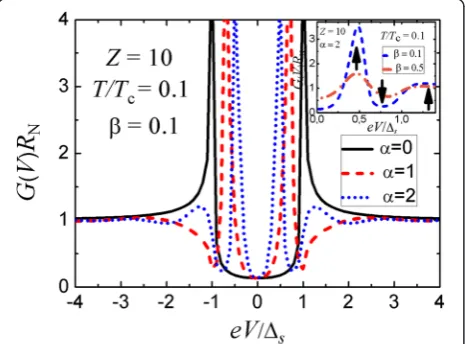
Figure 1 exhibits differential-conductance curves for a planar three-dimensional N-I-n-S structure with an s -wave superconductor and a normal n interlayer where the probability to transfer barrier I is much less than unity (the tunneling regime). The impact of the n layer thickness dn and that of the mean free path ln is con-trolled by the parameters α= 2dnΔs/(ℏvF) and β=dn/ln, respectively. In the limit dn→0, we get a well-known
coherence peak in the differential-conductance curve at
[image:5.595.58.291.471.643.2]V=VΔ(Fig. 1, solid curve) that reflects the presence of a surface bound state in the n interlayer of a vanishing thickness, i.e., at the IS interface. Its asymmetry arises due to the non-analytical behavior of the scattering am-plitudes reh(he)(ε) at ε=eVΔ. With increasing dn, the bound state formed due to the interference of electron and hole waves is shifted to lower voltages and a pro-nounced dip appears slightly below V=VΔ (Fig. 1, dashed curve). For larger dn, we can see the appearance of an additional hump structure (Fig. 1, dotted curve) above V=VΔ which reminds about the presence of a non-analytical square-root dependence of Andreev-reflection amplitudes (3). All three main elements of the peak-dip-hump structure are shown by arrows in the inset in Fig. 1 that illustrates the effect of the electron mean free path on the conductance spectra of the tun-neling N-I-n-S(s-wave) structure.
Figure 2 shows that the presence of a peak-dip-hump structure does not strongly depend on the barrier transparency. It is more pronounced in the tunneling regime (DI<< 1) but is well reproduced
Reh¼teeiφereheiφhth 1þrheiφh
rheeiφereeiφereheiφhþ…
¼ teeiφ eþiφh
rehth 1−rhe2iφeþ2iφh
rherehr′e; Ree¼reþteeiφereheiφhrheiφhrheeiφete 1þrheiφhrheeiφereeiφereheiφhþ…
¼reþ t
ee2iφeþ2iφh
rehrhrhete 1−rhe2iφeþ2iφh
rherehr′e;
ð6Þ
Fig. 1Main panel: Differential conductance-versus-voltage characteristics for a planar three-dimensional N-I-n-S(s-wave) junction with various thicknesses of the normal n interlayer in the tunneling regime (DI<< 1); parametersα= 2dnΔs/(ℏvF) andβ=dn/ln.Inset: Effect of the electron mean free path on the conductance spectra of a tunneling N-I-n-S(s-wave) four-layered device; the
three arrowsshow the main elements of the peak-dip-hump structure discussed in the text
Fig. 2Main panel: Effect of the barrier transparency on the peak-dip-hump structure in conductance spectra of a planar three-dimensional N-I-n-S(s-wave) junction; parametersα= 2dnΔs/(ℏvF) and
[image:5.595.305.539.492.664.2]even for a high-transparency device with DI= 0.5. As
is expected, the temperature and charge scattering processes significantly destroy the anomalous features (see the insets in Figs. 1 and 2).
Before turning to novel high-temperature superconduc-tors, let us discuss old experiments on four-layered N-I-n-S structures having the n interlayer for sure. Here, we refer to three papers with n = Cu and S = Pb [24, 25] as well as with n = Al and S = NbZr alloy [26]. In the first paper [24], the authors studied Cu-Pb sandwiches with a 500-nm-thick lead film and copper interlayers of different thicknesses. At 0.06 K, they observed a sharp dip at about the lead energy gap fordCubetween 40 and 120 nm, and for higher
thick-nesses, the amplitude of the singularity was vanishing, probably due to the impurity scattering inside the Cu inter-layer [24]. These results were confirmed in ref. [25] fordCu
= 35 and 75 nm and dPb= 700 nm. The authors [24, 25]
tried to interpret their data within the McMillan tunneling model of the superconducting proximity effect [9] but ex-perienced large discrepancies, in particular in the dip re-gion. To explain them, the authors of ref. [24] supposed that the dip is the result of quasiparticle interference in the copper interlayer. Our simulations, Figs. 1 and 2, are based just on this assumption and qualitatively agree with the data shown in [24–26]. Measurements of In-I-Al-NbZr alloy junctions [26] also revealed the peak-dip structure that was interpreted as a bound state within the Al interlayer. Notice that additional peaks and dips in the differential conductance of tunnel junctions in ref. [26] can arise due to resonant tunneling processes across localized states in the interlayer [27].
Further confirmation of the bound-state assertion for the conductance peak came from an experiment [28] with a ferromagnetic (F) nanometer-thick film which re-placed the normal interlayer in the four-layered junction. In this case, the charge reflected at the F-S interface is created in the electron density of states with a spin op-posite to that of the incident quasiparticle and Eq. (1) is modified as follows
Δφs¼k↑FxdFþχeh−k↓FxdFþπ−k↓FxdFþχheþk↑FxdFþπ ¼2δkð ÞxFdF−2 arccosðε=ΔSÞ ¼2ππ
Since, for example, the difference in wave vectors
δkð ÞF ¼k↑F−k↓F in Ni is of the order of several nm−
1
, effects very similar to those predicted for N-I-n-S junctions with dn of the order of tens of nanometers can be now observed in N-I-F-S ones with a few nanometer-thick Ni interlayer. Indeed, an anomalous
“double-peak” conductance feature revealed in ref. [28] at V near ΔNb/e, in our opinion, is a
peak-dip-hump structure with a maximum strongly smeared by local inhomogeneities within the F interlayer.
[image:6.595.307.539.88.258.2]We should note that the calculations shown in Fig. 1 relate to a conventional s-wave supercon-ductor while the peak-dip-hump structure was re-vealed in high-Tc cuprates with d-wave pairing.
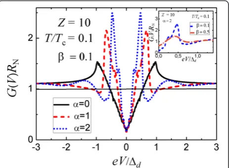
Thus, we should now discuss the latter case where the order parameter is an angle function Δ(θ) =Δd cos[2(θ−γ)]. If the misorientation angle γ= 0, we have the same phase shift (1) as in the conventional
s-wave superconductor with the only exception, the Fig. 3Main panel: Differential conductance-versus-voltage characteristics for a planar three-dimensional N-I-n-S(d-wave) structure with different thicknesses of the normal n interlayer in the tunneling regime (DI<< 1); the angleγ= 0; parametersα= 2dnΔd/(ℏvF) andβ=dn/ln.Inset: Effect of the electron mean free path on the conductance spectra of the tunneling N-I-n-S(d-wave) structure
Fig. 4Main panel: Differential conductance-versus-voltage characteristics for a planar three-dimensional N-I-n-S(d-wave) structure with different thicknesses of the normal n interlayer in the tunneling regime (DI<< 1); the angleγ= 45°; parametersα= 2d
[image:6.595.306.539.489.664.2]angle dependence of the gap parameter Δ θ~ð Þ ¼Δd
cos 2ð Þθ . The conductance spectrum for such an orientation is shown in Fig. 3. As in the case of an
s-wave superconductor, it exhibits a peak-dip-hump structure for sufficiently thick normal interlayers. On the contrary, if γ=π/4, we get the following expres-sion for the angle-dependent phase shift
Δφd¼ 4ε
ℏvF
dn
cosθ−2 arccos
ε Δdjsin 2ð Þθ j
−πþ2π;
ð7Þ
It is important that for such film orientation, inde-pendently on the n layer thickness dn, the phase shift
Δφd vanishes atε= 0. Hence, in this case, we should al-ways observe a zero-bias peak which is known to be ad -wave superconductivity indicator [29]. For comparatively thick interlayers, in addition to the zero-bias anomaly, we register, at first, a small peak at voltage biasVΔ and with the further increase ofdn, the emergence of a peak-dip-hump structure, see Fig. 4.
Since high-Tc samples are often composites of ran-domly oriented superconducting grains, we predict that, in the presence of an additional n interlayer, their con-ductance spectra should exhibit a pronounced peak-dip-hump structure which is present in all orientations and a weak zero-bias anomaly specific for a certain tunneling direction.
Transport Characteristics of S-n-I-n-S Junctions
Physical mechanisms of the charge transmission across heterostructures with two superconducting
electrodes are more complicated. In this section, we limit ourselves to s-wave pairing taking into account the fact that, after averaging over the realizations of the disorder, the order parameter in composites of randomly oriented superconducting grains with d -wave paring has global s--wave symmetry [30].
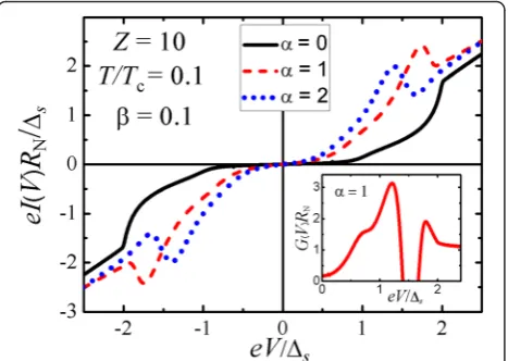
Let us start with the simplest tunneling transmission processes in S-n-I-n-S junctions. The presence of bound states at the electrode surfaces gives rise to unusual fea-tures in transport characteristics when the energies of the discrete levels align by applying the external bias. When properly aligned, we get the tunneling current peak and a negative differential resistance just above the resonant bias. Our calculations were done using a standard formula for tunneling current in a symmet-ric S-n-I-n-S configuration [1] where the tunneling density of states should be replaced by the electron penetration probability (5). The results are shown in Fig. 5. Calculated current-voltage characteristic for a three-dimensional S-n-I-n-S junction well reproduces the “knee” feature, see the “Background” section. Moreover, the first derivative shown in the inset in Fig. 5 demonstrates a peak, a region of the negative differential conductance which can reveal itself as a dip, and a hump at V= 2Δs/e. Note that just the pos-ition of the hump but not that of the peak deter-mines the doubled value of the energy gap Δs in the studied s-wave superconductor.
Now, let us discuss a high-transparency junction formed by two superconductors with degraded sur-faces. When the length of the transition region be-tween the two superconducting electrodes is less than elastic and inelastic lengths, we can again describe
Fig. 5Main panel: Current-voltage characteristics for a planar three-dimensional S-n-I-n-S junction with identicals-wave superconductors and various thicknesses of the normal n interlayer in the tunneling regime (DI<< 1).Inset: Conductance spectra of the S-n-I-n-S device,α= 1
Fig. 6Differential conductance-versus-voltage spectra for a planar S-n-I-n-S junction with identicals-wave superconductors and high-transparency transition region (DI= 0.7) without n interlayer (α= 0) and for a finite thickness of the normal n interlayer.Shaded regions
show positions of the 2Δs/nfeatures (peaksin the first case anddips
[image:7.595.306.538.501.664.2] [image:7.595.58.292.516.682.2]the transport across the device in terms of Andreev-reflection amplitudes and barrier scattering character-istics. But in this case, comparing to the tunneling regime, a new specific feature largely complicates the calculations. Let us look at an electron-like quasipar-ticle injected, for example, from the left electrode. Its energy after transferring the barrier is increased by
eV. The Andreev-reflected hole-like excitation is mov-ing in the opposite direction to that of the injected electron, and because of the opposite charge sign, its energy also increases by eV after the transmission across the barrier. These scattering events will con-tinue back and forth in the normal interspace be-tween the superconductors, and, as a result, each round trip of an electron-like quasiparticle will in-crease its energy by the value of 2eV. Finally, from each side of the barrier, we get an infinite set of scat-tering states with different energies shifted by 2eV. It results in recurrence relations for amplitudes of electron-like and hole-like wave functions which have been solved numerically. Our numerical simulations at zero temperature repeated in general terms similar calculations developed earlier [20, 31–33] with the only exception of the presence of an additional phase shift originated from charge passages across the n interlayer. Due to the standard theory of multiple Andreev reflections, the peaks positions in the conduct-ance spectra are determined by the formula Vn= 2Δs/n where n is an integer. Account of the additional phase shifts in the degraded near-surface regions replaces the peaks by dips (see Fig. 6). It is just what was found in ref. [14] and some previous publications for related Nb-based samples. The difference between Al-based junctions that follow the conventional theory [3] and Nb-based struc-tures which contradict it arises from the existence of a proximity layer, either normal, or superconducting with reduced critical temperature, at the surface of a supercon-ducting Nb film whereas the Al layer is usually not spoiled.
Conclusions
We have presented a scattering-like approach for study-ing Andreev bound states in a normal interlayer within ballistic superconducting heterostructures. Calculated transport characteristics of such devices exhibit a rich diversity of anomalous (from the viewpoint of the stand-ard theory) transport characteristics, in particular shift of differential-conductance maxima at gap voltages to lower positions and appearance of well-defined dips in-stead expected coherence peaks. We have compared our results with related experimental data and explained unexpected features observed in transport characteristics of heterostructures with transition metals and novel superconductors as an effect of the additional
non-superconducting interlayer at their surfaces. Note that our results are qualitatively similar to those obtained by other authors in the framework of physical assumptions that significantly differ from ours [8, 34, 35].
Competing Interests
The authors declare that they have no competing interests.
Authors’contributions
All authors contributed equally, read and approved the final manuscript.
Acknowledgements
This work was performed within the German-Ukrainian project SE 664/18-1 supported by Deutsche Forschungsgemeinschaft (DFG) and within the grant No. 612600 LIMACONA“Light-Matter Coupling in Composite Nano-Structures” supported by the EU Seventh Framework Programme. I.D. acknowledges financial support from the Russian Foundation for Basic Research, projects 13-02-01085 and 15-52-50054, and financial support from the Ministry of Education and Science of the Russian Federation, contract 14.Y26.31.0007.
Author details
1
Donetsk Institute for Physics and Engineering, National Academy of Sciences of Ukraine, 03039 Kyiv, Ukraine.2Skobeltsyn Institute of Nuclear Physics, Lomonosov Moscow State University, 119991 Moscow, Russia. 3Moscow Institute of Physics and Technology, 141700 Dolgoprudny, Moscow
region, Russia.4Institut für Festkörpertheorie und -optik,
Friedrich-Schiller-Universität Jena, 07743 Jena, Germany.5Institute for Metal Physics, National Academy of Sciences of Ukraine, 03680 Kyiv, Ukraine. 6Institut für Festkörperphysik, Friedrich-Schiller-Universität Jena, 07743 Jena,
Germany.
Received: 8 November 2015 Accepted: 26 January 2016
References
1. Wolf EL (2012) Principles of electron tunneling spectroscopy, 2nd edn. Oxford University Press, Oxford
2. Blonder GE, Tinkham M, Klapwijk TM (1982) Transition from metallic to tunneling regimes in superconducting microconstrictions: excess current, charge imbalance, and supercurrent conversion. Phys Rev B 25:4515–4532 3. Octavio M, Tinkham M, Blonder GE, Klapwijk TM (1983) Subharmonic
energy-gap structure in superconducting constrictions. Phys Rev B 27: 6739–6746
4. Nordman JE, Keller WM (1971) Controlled fabrication of Nb superconductive tunnel junctions with anomalous negative resistance. Phys Lett A 36:52–53 5. Tolpygo SK, Amparo D (2008) Electrical stress effect on Josephson
tunneling through ultrathin AlOxbarrier in Nb/Al/AlOx/Nb junctions. J
Appl Phys 104:063904
6. Schwidtal K (1972) Dc and ac Josephson effect in sputtered Nb-NbOx-Pb
junctions. J Appl Phys 43:202–208
7. Dettmann F, Pertsch P (1979) Nb-NbOx-PbIn tunnel junctions with ultra-thin
niobium electrodes. Phys Status Solidi A 52:Kl7–Kl20
8. Seidel P, Richter J (1980) Theoretical investigation of the current-voltage characteristics of superconducting niobium-lead tunnel junctions. Phys Status Solidi B 98:l89–l97
9. McMillan WL (1968) Tunneling model of the superconducting proximity effect. Phys Rev 175:537–542
10. Geiges T (2005) Tunnelling experiments in highTcsuperconductors: intrinsic and heating effects. PhD Thesis, Lausanne, EPFL., http:// infoscience.epfl.ch/record/53669
11. Ding H, Bellman AF, Campuzano JC, Randeria M, Norman MR, Yokoya T et al (1996) Electronic excitations in Bi2Sr2CaCu2O8: Fermi surface, dispersion, and absence of bilayer splitting. Phys Rev Lett 76:1533–1536
12. Norman MR, Ding H (1998) Collective modes and the superconducting-state spectral function of Bi2Sr2CaCu2O8. Phys Rev B 57:R11089–R11092 13. Zasadzinski JF, Ozyuzer L, Miyakawa N, Gray KE, Hinks DG, Kendziora C
(2001) Correlation of tunneling spectra in Bi2Sr2CaCu2O8+δwith the resonance spin excitation. Phys Rev Lett 87:067005
reflection in asymmetric superconductor/nanowire junctions. Nano Lett 14: 4977–4981
15. van Houten H, Beenakker CWJ. Andreev reflection and the Josephson effect in a quantum point contact: An analogy with phase-conjugating resonators. Physica B, 1991;175:187–97.
16. Andreev AF (1964) Thermal conductivity of the intermediate state of superconductors. Sov Phys JETP 19:1228–1231
17. Yang F, Liu R-B (2015) Geometric diffusion of quantum trajectories. Sci Rep 5:12109
18. Likharev KK (1979) Superconducting weak links. Rev Mod Phys 51:101–159 19. Landau LD, Lifshitz EM (1977) Quantum mechanics: non-relativistic theory,
vol. 3, 3rd edn. Pergamon Press, Oxford
20. Averin D, Bardas A (1995) ac Josephson effect in a single quantum channel. Phys Rev Lett 75:1831–1834
21. Anantram MP, Datta S (1996) Current fluctuations in mesoscopic systems with Andreev scattering. Phys Rev B 53:16390–16402
22. Belogolovskii M (2003) Phase-coherent charge transport in superconducting heterocontacts. Phys Rev B 67:100503
23. Devyatov IA, Goncharov DV, Kupriyanov MY (2001) Current transport in two-dimensional HTS NID junctions. Physica C 350:249–260
24. Freake SM, Adkins CJ (1969) Excitation spectrum induced by the proximity effect between copper and superconducting lead. Phys Lett 29A:382–383 25. Prothero DH (1974) Superconducting proximity effect in copper-lead
sandwiches. Philos Mag 29:829–846
26. Delesclefs R, Fischer O (1983) Tunneling studies of superconducting Nb-Zr/ Al proximity layers. J Low Temp Phys 53:339–358
27. Devyatov IA, Kupriyanov MY (1998) Current-voltage characteristics of SIS structures with localized states in the material of the barrier layer. JETP 87:375–381
28. SanGiorgio P, Reymond S, Beasley MR, Kwon JH, Char K (2008) Anomalous double peak structure in superconductor/ferromagnet tunneling density of states. Phys Rev Lett 100:237002
29. Kashiwaya S, Tanaka Y (2000) Tunnelling effects on surface bound states in unconventional superconductors. Rep Prog Phys 63:1641–1724
30. Kivelson SA, Spivak B (2015) Macroscopic character of composite high temperature superconducting wires. Phys Rev B 92:184502
31. Bratus’EN, Shumeiko VS, Wendin G (1995) Theory of subharmonic gap structure in superconducting mesoscopic tunnel contacts. Phys Rev Lett 74: 2110–2113
32. Hurd M, Datta S, Bagwell PF (1996) Current-voltage relation for asymmetric ballistic superconducting junctions. Phys Rev B 54:6557–6567
33. Hurd M, Löfwander T, Johansson G, Wendin G (1999) ac Josephson effect in superconductingd-wave junctions. Phys Rev B 59:4412–4426
34. Cuevas JC, Hammer J, Kopu J, Viljas JK, Eschrig M (2006) Proximity effect and multiple Andreev reflections in diffusive superconductor– normal-metal–superconductor junctions. Phys Rev B 73:184505
35. Aminov BA, Golubov AA, Kupriyanov MY (1996) Quasiparticle current in ballistic constrictions with finite transparencies of interfaces. Phys Rev B 53:365–373
Submit your manuscript to a
journal and benefi t from:
7 Convenient online submission 7 Rigorous peer review
7 Immediate publication on acceptance 7 Open access: articles freely available online 7 High visibility within the fi eld
7 Retaining the copyright to your article