Journal of Chemical and Pharmaceutical Research, 2014, 6(6):2659-2667
Research Article
ISSN : 0975-7384
CODEN(USA) : JCPRC5
Study on embedded optical sensor data collection and signal processing
1
Shi Shuheng and
2Wang Wenfan
1
Machinery institute, North China University of Water Resources and Electric Power, Zhengzhou, Henna, China 2
School of Information Engineering, Shengda Economics Trade & Management College of Zhengzhou, China _____________________________________________________________________________________________
ABSTRACT
This paper mainly completed the photoelectric signal data acquisition and design based on the embedded man-machine interactive interface, combined with the characteristics of all kinds of photoelectric sensors and photoelectric signal data, complete the design requirement of this system. Through the study of the photoelectric signal acquisition module, completed the design of optoelectronic devices, DC motor and CCD measurement circuit, the adjustment preamplifier circuit signal acquisition photoelectric signal. By using ARM9 and DSP data acquisition circuit, completed the CCD for data acquisition and analysis object after measurement. This approach not only give full play to the superiority of the DSP signal processing, but also for the follow-up to the main platform of ARM9 showed very good help design. We completed USB driver in the embedded system, Ethernet driver and touch screen driver, built the foundation for the realization of human-computer interaction platform to platform better. The main control platform WINCE operating system in the preparation of the man-machine interface, the experimental operation is simple and intuitive. Graphics interface to complete the experiment results, and the photoelectric characteristic curve is portrayed in the two-dimensional coordinate system, the user can see better and understand the experimental results.
Keywords: Integral equation; Embedded sensor system; Green function; Optical; Software Configuration
_____________________________________________________________________________________________
INTRODUCTION
The light source is an indispensable part in the photoelectric detection system, the system can according to the actual need to select with a certain radiation power, a spectral range and spatial distribution of the light source, beam in order to send as carrying information to be detected substances [1]. Sometimes the light source itself is the object to be measured, the light source is broad, can be artificial light source, also can be the natural light; transmission field is light propagation medium, such as air, water, waveguide, to consider the attenuation coefficient, background noise and other factors [2]. The receiving system function is to convert the optical signal to electrical signal, and the photoelectric detector is to accept the core parts of the system, the performance of detection capability and detection precision of the photoelectric detection system relies heavily on the photoelectric detector [3].
With the development of science and technology, communication technology and automation technology has been widely used in the industrial production, the photoelectric conversion and data acquisition technology is an important part of the communication technology and industrial automation, is difficult to substitute other technology [4]. The photoelectric conversion is mainly related to the stability and precision of photoelectric sensor, photoelectric converter directly affects the stability and control accuracy of automatic control, because of the diversity and complexity of the production environment of the detection object, photoelectric sensor and design corresponding to meet production needs, achieve in the actual environment conditions of high precision detection is very important [5-7].
gradually formed a photoelectron industry giant [8]. Technology development that promotes the infiltration and combination of optical technology and electronics technology, formed a comprehensive utilization of hybrid system optical and electronic technology, referred to as the photoelectric system [9]. Here, a variety of optical, optoelectronics based on electro-optic, optically active controllable devices play a decisive role, they communicate the optical and electronic system connections.
This paper uses ARM as the core, to realize the data acquisition circuit of photoelectric signal by photoelectric detection processing of photoelectric signal of the photoelectric sensor induction of various basic to, and through the study of DSP and ARM interface technology to achieve high speed acquisition of photoelectric signal data. The experimental results quantitatively show that the use of ARM9, to achieve a good human-computer interaction function. According to the principle of photoelectric detection, the main contents of this paper are as follows:
(1) The design of photoelectric detection circuit design of function module, photoelectric properties including photoelectric detectors.
(2) High speed implementation of design, data acquisition module based on DSP Precise data collection, digital signal processing using TMS320LF2407 chip TI conversion, and the processed data are transferred to ARM. (3) The transplant of embedded operating system, debug, and driven programming, project selection. This paper uses Samsung 53C2440 as the main control system unit to complete the sampling and displaying photoelectric signal data received by WINCE system in s3C2440.
(4) The design of ARM9 interface, including a touch screen USB, Network port driver by WCE and compiler software was designed of experiment operation interface, to achieve human-computer interaction better.
I. THE THEORETICAL BASIS OF THE PHOTOELECTRIC DETECT ION SYSTEM A. The principle and classification of photoelectric detector
(1) The dark resistance and light resistance
This is one of the most important parameters of photosensitive resistance performance, the so-called dark resistance refers to the measured resistance without light irradiation value [10]. Then at a given voltage, current flowing through the photosensitive resistor called dark current. In the light irradiation, the photosensitive resistor called bright resistance, the current time the bright current. The difference on current and dark current is called light current. Obviously, light resistance and dark resistance difference bigger, higher photocurrent, higher sensitivity, the better the performance of photosensitive resistance. The utility of photosensitive resistance, the dark resistance is often more than dozens of M, and even up to 100M, and bright resistance in thousands of Europe.
2
( )
1 (3
)
(
)
VF
VF
A sCR
A s
A
sCR
sCR
(1)
3
VF O
VF
A
A
A
(2)
0
1/ (
RC
)
(3)
1/ (3
VF)
Q
A
(4)
10 20 30
120 200
()
I
m
A
( ) U V
0
40 80 160
10lx 100lx
1000lx
Power 500mW
Figure 1. The volt ampere characteristic of photosensitive resistance
In a certain light illumination, and between the photosensitive resistor at both ends of the voltage and current of the light curve, called the volt ampere characteristic of photosensitive resistance, was shown in Figure 1. As can be seen, the photocurrent increases with increasing applied voltage, and no saturation phenomenon, the applied voltage to a certain value, enhance the value of photo current with the light increases. When in use, the photosensitive resistance by the power dissipation limits, at both ends of the voltage does not exceed the maximum working voltage, the dotted line to allow the power curve, which can determine the normal working voltage sensitive resistor.
(3) Light
Under certain applied voltage, current and flux curve light photosensitive resistor between F, called light, as shown in Figure 2. From the map view, the curve is nonlinear, therefore not suitable for quantitative detection of photosensitive resistance element, and often is used as the photoelectric switch in automatic control.
10 20 30 40 50 500 1000 ( )
IA
( )
[image:3.595.218.392.214.350.2]L lx
Figure 2. Flux curve light photosensitive resistor
B. The main parameters and basic characteristics of photosensitive resistance
Photosensitive diode illumination characteristics as shown in Figure 3, it presents the relationship between the photocurrent and the illumination of the photosensitive diode. Photosensitive diode linear illumination characteristics can be seen from the graph.
0.05 0.10 0.15 0.20 0.25 0.6 () I m A 0
(lm)
0.2 0.4 0.8 1.0
Figure 3. Photosensitive diode illumination characteristics 0 -1 -2 -3 -4 -5
-6 50 10
0 15 0 20 0 V/ V V/mV -5 -10 -15 -20 -25 ( ) IA
Reverse Bias Voltage Unbiased Voltage 0 P 1 P 2P 3 P 4 L small R L large R
The volt ampere characteristic of the photosensitive diode refers to the current voltage characteristics in a certain light. The volt ampere characteristic of the photosensitive diode was shown in Figure 4, it can be seen from the figure, in the absence of bias, photosensitive diode is still light output current, which is decided by the nature of the photoelectric effect of the photosensitive diode.
C. The main parameters of the photosensitive diode and the basic characteristics
Photoconductive detector photoelectric photoelectron effect is the most widely be used, the interaction of the incident radiation and the lattice atoms or impurity atoms bound electron, free electrons generated one pairs. Free electrons or holes, so that the carrier excitation of the semiconductor conductivity and the photon remains inside the material, so the photoconductivity is one kind of the photoelectric effect. Intrinsic need photon excited electron hole pairs, the photon energy at least and band width, so the basic requirement is
K
hv
E
(5)
So the long wave limit field optical conductivity is
0
hc E
/
K
(6)
Non intrinsic long wave optical limiting conductance is
0
1.24 /
E
i
(7)
D. The performance parameters of photoelectric detector
Responsiveness responsive is description parameters of the sensitivity of the detector, the relation between parameters which characterize the detector output signal and the input radiation, defined as the output of photo detector voltage Vs or RMS current Is and the incident to the average optical power detector on the ratio, and Rv and Ri in mind.
/
(V/W)
V SR
V
P
(8)
/
(A/W)
I S
R
I
P
(9)
Monochromatic sensitivity: monochromatic sensitivity and spectral, with all said, is the output voltage of photoelectric detector or the current incident on the detector with monochromatic radiation flux (flux) ratio:
/
( ) (V/ W)
V SR
V
(10)
/
( ) (A/W)
I S
R
I
(11)
The time constant can be obtained and the incident radiation modulation frequency response of photoelectric, and its expression is
2 1/2 0
( )
/ [1 (2
) ]
R f
R
f
(12)
When Rf/R0 = 0.707, available amplifier upper cut-off frequency
1/ 2
1/ 2
f
RC
(13)Signal to noise ratio (S/N) is to determine parameters of noise size commonly used, it is in the signal power load resistance produced on RL and noise power ratio:
2 2 2 2
/
S/
N S L/
N L S/
NS N
P
P
I R
I R
I
I
(14)
If the measured in decibels 2 2
II. SYSTEM DESIGN AND SIGNAL PROCESS A. USB driver design
USB bus uses polling control, host control setup initializes all the data transmission of USB bus implementation of each transmission action can transmit three packets. At the beginning of each transmission, the sending host controller a descriptor to describe the type and direction of movement of the transmission, the packet is called mark packets. USB device receives (Figure 5) the host sends the token packet the analytical data of their data.
Physical Device
Special Communication Equipment
Logical Device
USB Data Framework
Bus Interface
Special Driver Channel
Default Pipe
USB Cable
USB Device Driver Program
Non-USB Fromat
USBD Module
USB Data Framework
[image:5.595.189.519.152.352.2]USB Adapter /Controller
Figure 5. USB transmission mode
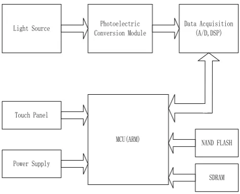
B. The system hardware circuit design
In determining a good two main processor of the system, is to analyze the peripheral circuit design based on the processor to realize the function of the system, mainly consists of power module, optical module, data acquisition module and main control module. The light source, the design of the main function modules in the photoelectric principle and characteristics of various optoelectronic devices are the analysis, research, according to the electric signal photoelectric sensor output basic variety, complete pre circuit signal processing. The data acquisition module is mainly used for the analog signal acquisition circuit came for subsequent processing, analog signals into digital signal through the DSP's built-in A/D converter. The main control unit module comprises a power supply circuit chip the power supply, storage module and storage of experimental data and run the operating system. The overall design of the hardware circuit system was shown in Figure 6.
MCU(ARM) Touch Panel
Power Supply
NAND FLASH
SDRAM Data Acquisition
(A/D,DSP) Photoelectric
Conversion Module Light Source
Figure 6. The overall design of the hardware circuit system
[image:5.595.187.424.502.693.2]emitting light wavelength in a certain distribution, spectral line with mode structure is obvious. Infrared light emitting diode parameters was shown in Table 1.
Table 1. Infrared light emitting diode parameters
Parameter Test Condition Value Unit Min Type Max Forward Voltage
I
50mA
— 1.5 1.8 V Reverse CurrentV
9V
— — 10 uA Peak WavelengthI
50mA
— 850 — nm Spectral Line half-widthI
50mA
— 45 — nm Radiant IntensityI
50mA
80 100 — mV/Sr Viewing AngleI
20mA
— 10 — degC. The system software design
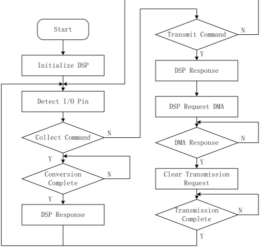
DSP analog-to-digital conversion process is DSP analog-to-digital conversion module in accepting the start signal according to the modulus of order set pre conversion process. The collected signal is stored in the internal memory, the software program flow chart (Figure 7).
Start
Initialize DSP
Detect I/O Pin
Collect Command
Conversion Complete
DSP Response
Transmit Command
DSP Response
DSP Request DMA
DMA Response
Clear Transmission Request
Transmission Complete Y
Y
Y
Y Y
N
N
[image:6.595.179.435.289.530.2]N N N
Figure 7. The software program flow chart
III. EXPERIMENTAL RESULTS A. Software configuration process
The microprocessor software configuration process was shown in Figure 8, power system, firstly, such as self, the initial work; then, check the save EEPROM vector hardware configuration data is normal (hand considering the vector hardware service life, on the other hand to both data security and power supply system etc.), after the is reading the configuration data in EEPROM.
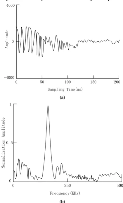
B. Study on signal denoising
Start
Boot Initialization
Check EEPROM is Normal?
Check the Special Flag In EEPROM?
Read the Configuration Data in EEPROM Read the Default
Configuration Data from ROM as Configuration Dat
1 Read Default Configuration Data from ROM
2 Save Default Configuration Data to EEPROM 3 Write Special Flag
Subsequent Sections Main Program Cycle
Yes
Yes
No No
[image:7.595.199.410.408.754.2]Figure 8. The microprocessor software configuration process
50
0 100 150 200
0
-4000 4000
A
m
p
l
i
t
u
d
e
Sampling Time(us)
(a)
0 250 500
0.5
0 1
N
o
r
m
a
l
i
z
a
t
i
o
n
A
m
p
l
i
t
u
d
e
C. The simulation and debugging of the microprocessor system
Hardware test and debug of the system mainly include the following aspects:
(1) Check the electrolytic capacitor, diode and a light emitting diode polarity is correct; (2) Check the integrated circuit socket direction is correct;
(3) Check each component pin whether there is leakage welding, weld or solder adhesion (short circuit); (4) From the test +5V power test, 3.3V and 1.8V power supply is correct;
(5) The signal from the reset test RnST J2 is normal;
(6) Tested by crystal oscillator pins, check whether the crystal oscillator; (7) Check each jumper settings are correct;
D. System interface design
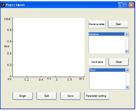
WMLBUTTONDOWN is triggered when the user presses the left mouse button, the pop-up box. A cancellation message in GWES, message queues, and window between the message loop process flow as shown in Figure 10.
[image:8.595.191.422.254.442.2]Finally, to complete the man-machine interface was shown below:
Figure 10. The window between the message loop process flow
CONCLUSION
After consulting domestic and foreign large number of references, the acoustic emission signal processing methods are summarized. Aiming at the problem of acoustic emission signal processing field, some problems and key technologies are studied. Through the study of the photoelectric signal acquisition module, completed the design of optoelectronic devices, DC motor and CCD measurement circuit, the adjusting circuit signal acquisition photoelectric signal. By using ARM9 and DSP data acquisition circuit, completed the CCD for data acquisition and analysis object after measurement. This approach not only give full play to the superiority of the DSP signal processing, but also for the follow-up to the main platform of ARM9 showed very good help design. We completed USB driver in embedded system, Ethernet Driver and touch screen driver, a basic platform for the realization of human-computer interaction platform need better.
REFERENCES
[1]Raskar R., Welch G., Cutts M., Lake A., Stesin L., and Fuchs H., The Office of the Future: A Unified Approach to Image-Based Modeling and Spatially Immersive Displays. Proceedings of the 25th annual conference on Computer graphics and interactive techniques, 1998: p. 179-188.
[2]Ashdown M., Flagg M., Sukthankar R., and Rehg J.M., A Flexible Projector-Camera System for Multi-Planar Displays, Computer Vision and Pattern Recognition (CVPR). 2004.
[3]Brown M.S. and Seales W. A Practical and Flexible Tiled Display System 10th Pacific Conference on Computer Graphics and Applications (PG'02). 2002.
[4]Li K., Chen H., Chen Y., Clark D.W., Cook P., Damianakis S., Essl G., Finkelstein A., Funkhouser T., and Housel T., Building and Using a Scalable Display Wall System. Computer Graphics and Applications, IEEE, 2000. 20(4): p. 29-37.
[6]Wei B., Silva C., Koutsofios E., Krishnan S., and North S., Visualization Research with Large Displays. IEEE Computer Graphics and Applications, 2000. 20(4): p. 50-54.
[7]Chen Y., Clark D.W., Finkelstein A., Housel T.C., and Li K., Automatic Alignment of High-Resolution Multi-Projector Display Using an Un-Calibrated Camera. Proceedings of the conference on Visualization'00, 2000: p. 125-130.
[8]10. Chen H., Sukthankar R., Wallace G., and Li K., Scalable Alignment of Large-Format Multi-Projector Displays Using Camera Homography Trees. Proceedings of IEEE Visualization, 2002: p. 339-346.
[9]R Wildes, J. Asmutll, G Greell, S. Hsu, R. Kolczynski, J. Matey, S. Mcbride,” Machine vision and Applications, Vol 9, pp.1-8, 1996.