ISSN Online: 1942-0749 ISSN Print: 1942-0730
Experiment of Frequency Range Dependent
TE
10
to TE
20
Mode Converter
Yoshihiro Kokubo, Tadashi Kawai
Graduate School of Engineering, University of Hyogo, Himeji-shi, Hyogo, Japan
Abstract
Typical metallic waveguide mode converters convert electromagnetic waves from one mode to another mode for some frequency ranges. However, most electromag-netic waves outside of the specified frequency range are reflected. We report a design for a mode converter which passes the TE10 mode at a low frequency range and
effi-ciently converts the TE10 mode to the TE20 mode at a high frequency range. To
grad-ually shift the mode profile from TE10 to TE20, dielectric rods are placed in a sequence
along the waveguide starting near the sidewall and moving to the center of the wa-veguide with decreasing radius of the rods. This design reduces reflection of electro-magnetic waves. Experimental tests demonstrate the efficacy of the design.
Keywords
Waveguides, Dielectric Array, Scattering Parameter, Mode Converter
1. Introduction
We have reported that single-mode propagation is available for a metallic waveguide with dielectric rods arrayed at the center of the waveguide in the frequency under twice the cutoff frequency region using the TE10 mode, and in the frequency over twice the
cutoff frequency region using the TE20 mode, because of restrictions of the TE10 mode
[1] [2]. However, a TE20-like mode, which is propagated in the 2nd band, is an odd
mode, and generation systems for odd modes have seldom been reported.
In this investigation, we fabricate a mode converter, which passes through the TE10
mode for the low frequency range and efficiently converts TE10 to TE20 mode (or TE20 to
TE10 mode) for the high frequency range. Typical metallic waveguide mode converters
convert electromagnetic waves from one mode to another mode for some frequency range. However, most electromagnetic waves outside of the specified frequency range are reflected [3] [4].
How to cite this paper: Kokubo, Y. and Kawai, T. (2016) Experiment of Frequency Range Dependent TE10 to TE20 Mode
Conver-ter. Journal of Electromagnetic Analysis and Applications, 8, 173-181.
http://dx.doi.org/10.4236/jemaa.2016.89017
Received: August 4, 2016 Accepted: August 30, 2016 Published: September 2, 2016
Copyright © 2016 by authors and Scientific Research Publishing Inc. This work is licensed under the Creative Commons Attribution International License (CC BY 4.0).
http://creativecommons.org/licenses/by/4.0/
In a rectangular metallic waveguide, only the TE10 mode propagates for 0.5 < ωw/2πc
< 1 (the 1st band) for a given frequency ω, which is normalized using the width of the waveguide w. On the other hand, both the TE10 and TE20 modes can propagate for 1 <
ωw/2πc < 1.5 (the 2nd band), where c is the velocity of light in a vacuum. The TE10 and
TE20 modes have the same frequency ω, but different wave vectors k and group velocity
vg = (dk/dω)−1. When a mode in the 2nd band is converted from TE10 to TE20, the group
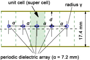
velocity of the electromagnetic wave changes. In the 1st band, it cannot be changed. We have previously reported a waveguide which restricts certain modes [5] and a prototype mode converter [6]. These devices consist of periodic dielectric rod arrays in a waveguide similar to that shown in Figure 1. However, it is not easy to determine the group velocity in the waveguide. The propagation modes in a waveguide having in-line dielectric rods with period a can be calculated using a supercell approach [7] by apply-ing appropriate periodic Bloch conditions at the boundary of the unit cell [8]. When the location of the dielectric rods is fixed at a distance d from the sidewall, the group velocity vg for both the 1st and 2nd bands can be changed by varying the radius r.
However, the group velocities for both bands are changed at the same time and cannot be changed individually. For d and r fixed to certain values, vg/c can be calculated for
the periodic structure of the dielectric rods at a specific frequency [9]. After calculating vg with pairs of d and r, each pair of d and r is combined.
2. Initial Design
We consider a metallic waveguide of size 17.4 × 8 mm2 (cutoff frequency f
c ≈ 8.62
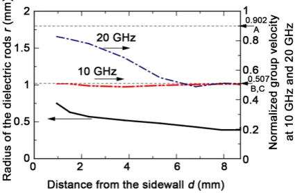
GHz). The period a is fixed at 7.2 mm for target frequencies of 10 GHz (1st band) and 20 GHz (2nd band). Figure 2 shows a sample of the calculated normalized velocities along the axis of the waveguide at 10 GHz and 20 GHz for dielectric rods (LaAlO3: εr =
24, radius r (mm)) aligned at a distance from the sidewall d (mm). It is desirable that the normalized velocity vg/c = 0.902 (TE10: point A) monotonically decrease to vg/c =
0.507 (TE20: point B) at 20 GHz, and that the normalized velocity vg/c = 0.507 (TE10:
[image:2.595.294.453.582.688.2]point C) be unchanged at 10 GHz. However, at 20 GHz, such a condition is not found around d = 6 - 7 mm, because the placement of the dielectric rods at the center of the waveguide minimizes the electric field. On the other hand, placing the dielectric rods near the sidewall of the waveguide maximizes the electric field. At the transition region, around d = 6 - 7 mm, the characteristics are complex. A priority of the design is that the
Figure 2. Group velocity in a metallic waveguide with a periodic array of dielectric rods for vari-ous distances from the sidewall d and varivari-ous radii of the rods r, at 20 and 10 GHz.
group velocity at 10 GHz not change. Since the group velocity decreases for dielectric material at 10 GHz and becomes slowest at d = 3 mm, the design employs the 20 GHz frequency for mode conversion, because both the 20 GHz and 10 GHz conditions can-not be satisfied at the same time.
Figure 3 shows the layout of the rods (though note that rods 0 and 10 are not in-cluded in the prototype, but are additions, as detailed below). Since the mode profile gradually shifts from TE10 to TE20, the dielectric rods are placed progressively away
from near the sidewall to the center of the waveguide, as illustrated in the figure. The nine dielectric rods (i = 1 to 9) have decreasing radii ri and are placed constant distance
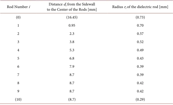
apart a = 7.2 mm. Three dielectric rods (i = 7, 8, and 9) are located at the center of the waveguide. Table 1 shows distances di and radii ri of the rods.
The S parameters between the input port (Port 1) and output port (Port 2) are calcu-lated using the HFSS software by Ansys [10], and the results are shown as dotted lines in Figure 4. The electromagnetic waves enter as the TE10 mode for 9.1 - 14.4 GHz and
are converted to the TE20 mode with 18.3 - 21.0 GHz with over 95% efficiency.
Howev-er, reflection of the TE10 mode at low frequencies and the TE20 mode at high frequencies
range are significant under −15 dB, and optimization of the design is necessary to re-duce reflection.
3. Decreasing the Reflection [9]
As shown in Figure 4, the reflection of the TE10 mode is significant around 10 to 14
GHz. This is because the rods located at the center of the waveguide are truncated at Port 2. Another dielectric rod located at the center of the waveguide (rod 10) is needed to decrease electromagnetic reflection. The rod has a smaller cross-section radius of r = 0.29 mm compared with rods 8 and 9. The reflection of the TE20 mode is also
signifi-cant around 18 to 20 GHz. This is because the rods are located asymmetrically at Port 1. To decrease reflection of the TE20 mode, another dielectric rod (rod 0) is placed on the
Figure 3. Proposed structure of the TE10 to TE20 mode converter (the prototype structure does
not have rod 0 (i = 0) and rod 10 (i = 10)).
Figure 4. S parameters for the mode converter, |S21| and |S11| (the dotted lines show the case
without rods 0 and 10. The solid lines are for the case with rods 0 and 10.).
Table 1. Location and radii of the dielectric rods.
Rod Number i Distance di from the Sidewall
to the Center of the Rods [mm] Radius ri of the dielectric rod [mm]
(0) (16.45) (0.73)
1 0.95 0.70
2 2.3 0.57
3 3.8 0.52
4 5.3 0.49
5 6.8 0.43
6 7.9 0.39
7 8.7 0.39
8 8.7 0.42
9 8.7 0.42
[image:4.595.267.480.265.428.2] [image:4.595.195.553.492.709.2]The S parameters between the input port (Port 1) and output port (Port 2) calculated using the HFSS are shown as solid lines in Figure 4.
4. Fabrication and Experimental Results
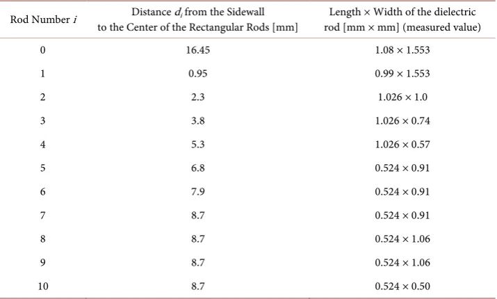
In fabricating a mode converter, such as the Type A illustrated in Figure 5(a), it is ne-cessary to install the dielectric rods in the waveguide without a gap at the top or bot-tom. Such a structure can be difficult to fabricate. In our approach, holes are machined at the top of the waveguide and the dielectric rods are inserted. For low-cost fabrica-tion, a rectangular dielectric rod quarried from a slab is more suitable than a column (Type B; Figure 5(b)). The rectangular dielectric rods are fabricated from slabs of LaAlO3 with thicknesses of 0.5, 1.0, and 1.5 mm, and are cut to give cross sections the
same as would be the case for columns. The dimensions of the dielectric rectangular rods are shown in Table 2.
A problem arises in that a typical coaxial-waveguide converter cannot detect the TE20
mode since an electrode is placed at the center of the waveguide. Our procedure to detect the TE20 mode is to first confirm that the TE10 mode does not propagate to the
[image:5.595.241.505.328.412.2](a) (b)
Figure 5. (a) Dielectric rod located in a waveguide without gaps at top and bottom; (b) Dielectric
rectangular rod inserted in a hole made at the top of the waveguide with a space of 0.02 mm be-tween the rods and the top wall of the waveguide. (a) Type A; (b) Type B.
Table 2. Locations and sizes of the dielectric rods arranged in Type B.
Rod Number i Distance di from the Sidewall
to the Center of the Rectangular Rods [mm] rod [mm × mm] (measured value) Length × Width of the dielectric
0 16.45 1.08 × 1.553
1 0.95 0.99 × 1.553
2 2.3 1.026 × 1.0
3 3.8 1.026 × 0.74
4 5.3 1.026 × 0.57
5 6.8 0.524 × 0.91
6 7.9 0.524 × 0.91
7 8.7 0.524 × 0.91
8 8.7 0.524 × 1.06
9 8.7 0.524 × 1.06
[image:5.595.196.554.490.705.2]end of the TE10 to TE20 mode converter at mode conversion frequency and then to
connect another mode converter of the same type to the original converter in the oppo-site direction and measure the reconverted TE10 from TE20 mode.
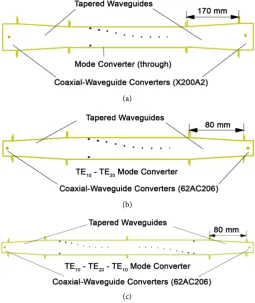
Fabricated mode converters have a full length of 130 mm. The outside appearance is shown in Figure 6 and the experimental setups are shown in Figures 7(a)-(c). Figure 7(a) is the setup for confirming that the TE10 mode has passed through the mode
[image:6.595.240.509.189.311.2]con-verter at the low frequency range. The mode concon-verter was connected to a HP-8510B
Figure 6. Frequency range dependent mode converter.
(a)
(b)
(c)
Figure 7. Experimental setup for measurement of S parameters. (a) |S21| and |S11| at low
frequen-cies; (b) |S21| (TE10 - TE10), |S11| (TE10 - TE20 - TE10) and |S22| (TE10 - TE10) at high frequencies. (c)
|S21| (TE10 - TE20 - TE10) and |S11| (TE10 - TE10, TE10 - TE20 - TE10 and TE10 - TE20 - TE10 - TE20 -
[image:6.595.245.501.347.651.2]network analyzer by a coaxial-waveguide converter (Maury Microwave X200A2: 8.2 - 12.4 GHz, VSWR max = 1.05) through a tapered waveguide of 170 mm length.
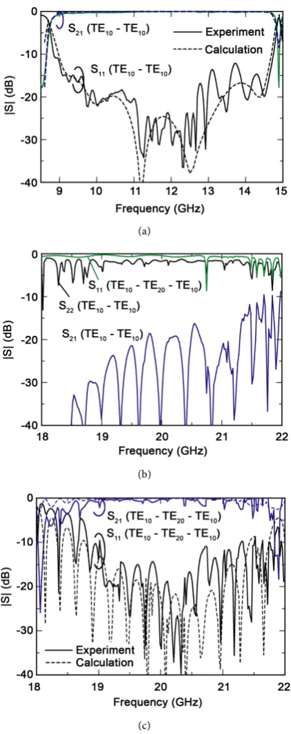
The experimental results are shown in Figure 8(a) as solid lines. The dotted lines in-dicate the calculated results and are sufficiently consistent with the experimental re-
(a)
(b)
[image:7.595.268.479.142.674.2](c)
Figure 8. Experiment results of S parameters: (a) |S21| and |S11| in Figure 7(a); (b) |S21|, |S11| and
sults. Figure 7(b) is the setup for confirming that the TE10 mode is converted to the
TE20 and that the TE10 is not propagated (the coaxial-waveguide converter is a Fairview
Microwave Inc. 62AC206: 12.4 - 18.0 GHz, VSWR max = 1.25). The experimental re-sults are shown in Figure 8(b) as solid lines. The figures show that S21 for the TE10
mode propagation is very small.
To measure the conversion efficiency from the TE10 to TE20 mode, another of the
same type of mode converter is connected in the opposite direction to the previous mode converter. The values of the S parameter S21 is the conversion efficiency after
converting from TE10 to TE20 and reconverting from TE20 to TE10. Figure 8(c) shows
the experimental results for the setup shown in Figure 7(c). The solid lines are experi-mental results and are almost the same as the calculation results shown as dotted lines.
5. Conclusion
We have proposed a frequency range dependent TE10 to TE20 mode converter that
effi-ciently converts the low frequency TE10 mode to the high frequency TE20 mode by small
variations of the group velocity of the TE10 mode. The mode converter allows low
fre-quency electromagnetic waves to pass through but converts higher frefre-quency electro-magnetic waves from the TE10 mode to TE20 mode without reflection. We demonstrate
that electromagnetic waves pass through in the TE10 mode at 9.7 - 14.6 GHz and are
converted to the TE20 mode at 19.1 - 20.3 GHz at over 95% efficiency. Such frequency
range dependent mode converters are useful for applications that require single-mode propagation at two frequencies.
Acknowledgements
The authors thank Mr. H. Miyazaki for help with the experiment set-up.
References
[1] Kokubo, Y. (2007) Wide Band Metallic Waveguide with In-Line Dielectric Rods. IEICE Transactions on Electronics, J90-C, 642-643. (In Japanese)
[2] Kokubo, Y. and Kawai, T. (2009) 90-Degree H-Plane Bent Waveguide Using Dielectric Rods. Microwave and Optical Technology Letters, 51, 2015-2017.
http://dx.doi.org/10.1002/mop.24573
[3] Zhang, Q., Yuan, C.W. and Liu, L. (2012) Theoretical Design and Analysis for TE20-TE10
Rectangular Waveguide Mode Converters. IEEE Transactions on Microwave Theory and Techniques, 60, 1018-1026. http://dx.doi.org/10.1109/TMTT.2011.2182206
[4] Xu, C., Tantawi, S. and Wang, J. (2014) Novel X Band Compact Waveguide Dual Circular Polarizer. Cornell University Library, 1406.7266.
[5] Kokubo, Y. (2008) Wide Band Metallic Waveguide with In-Line Dielectric Rods. IEEE Mi-crowave and Wireless Components Letters, 18, 79-81.
http://dx.doi.org/10.1109/LMWC.2007.915028
[6] Kokubo, Y. (2010) Frequency Range Dependent TE10 to TE20 Mode Converter. Microwave
and Optical Technology Letters, 52, 169-171. http://dx.doi.org/10.1002/mop.24886
Band-Gap Boundaries. Journal of Applied Physics, 79, 7483-7492. http://dx.doi.org/10.1063/1.362419
[8] Boroditsky, M., Coccioli, R. and Yablonovitch, E. (1998) Analysis of Photonic Crystals for Light Emitting Diodes Using the Finite Difference Time Domain Technique. Proceedings of SPIE, 3283, 184-190. http://dx.doi.org/10.1117/12.316682
[9] Kokubo, Y. (2011) Waveguide Mode Converters. Chapter 14, Electromagnetic Waves/Book 1, In-Tech, Vienna, 283-296. http://dx.doi.org/10.5772/16609
[10] Ansys, Inc. (2007) Achieve High-Frequency, High-Speed Component Design Tools from ANSYS. HFSS V11.
Submit or recommend next manuscript to SCIRP and we will provide best service for you:
Accepting pre-submission inquiries through Email, Facebook, LinkedIn, Twitter, etc. A wide selection of journals (inclusive of 9 subjects, more than 200 journals)
Providing 24-hour high-quality service User-friendly online submission system Fair and swift peer-review system
Efficient typesetting and proofreading procedure
Display of the result of downloads and visits, as well as the number of cited articles Maximum dissemination of your research work