Electronically-Controllable Grounded-Capacitor-Based
Grounded and Floating Inductance Simulated
Circuits Using VD-DIBAs
Data Ram Bhaskar
1*, Dinesh Prasad
1, Kanhaiya Lal Pushkar
21Department of Electronics and Communication Engineering, Faculty of Engineering and Technology, Jamia Millia Islamia, New Delhi, India
2Department of Electronics and Communication Engineering, Maharaja Agrasen Institute of Technology, Rohini, New Delhi, India
Email: *[email protected], [email protected], [email protected] Received July 17, 2013; revised August 17, 2013; accepted August 24, 2013
Copyright © 2013 Data Ram Bhaskar et al. This is an open access article distributed under the Creative Commons Attribution Li-cense, which permits unrestricted use, distribution, and reproduction in any medium, provided the original work is properly cited.
ABSTRACT
New Voltage Differencing Differential Input Buffered Amplifier (VD-DIBA) based lossless grounded and floating in-
ductance simulation circuits have been proposed. The proposed grounded simulated inductance circuit employs a single
VD-DIBA, one floating resistance and one grounded capacitor. The floating simulated inductance (FI) circuits employ
two VD-DIBAs with two passive components (one floating resistance and one grounded capacitor). The circuit for
grounded inductance does not require any realization conditions where as in case of floating inductance circuits, a sin-
gle matching condition is needed. Simulation results demonstrating the applications of the new simulated inductors us-
ing CMOS VD-DIBAs have been included to confirm the workability of the new circuits.
Keywords:
VD-DIBA; Inductance Simulation; Filters
1. Introduction
The importance of grounded and floating simulated in-
ductors in the context of active network synthesis is well
known [1]. Several grounded and floating inductance
simulation schemes, employing different active elements
such as operational amplifiers (op-amps) [2-6], current
conveyors (CCs) [7-15], current controlled conveyors
(CCCIIs) [16,17], current feedback operational amplifi-
ers (CFOAs) [18,19], operational mirrored amplifiers
(OMAs) [20], differential voltage current conveyors
(DVCCIIs) [21], current differencing buffered amplifiers
(CDBAs) [22,23], current differencing transconductance
amplifiers (CDTAs) [24,25], operational transconduc-
tance amplifiers (OTAs) [26,27] have been reported in
the literature. In [28], many new active building blocks
have been introduced; VD-DIBA is one of them. Till
now, some applications of VD-DIBAs have been re-
ported in the open literature such as in the realization of
all pass filters [29], realization of grounded and floating
inductance circuits using two/three VD-DIBAs as re-
ported in [30], electronically controllable sinusoidal os-
cillator in [31] and voltage-mode universal biquad in
[32,33]. The purpose of this paper is to introduce new
VD-DIBA-based: 1) a lossless grounded inductor using
only a single VD-DIBA, one resistor and a grounded
capacitor without requiring any matching condition and 2)
two floating inductance simulation circuits employing
two VD-DIBAs, one resistor and a grounded capacitor
along with a single matching condition for floatation.
The genesis of these FI circuits is inspired by [1,34,35].
2. The Proposed New Configuration
The schematic symbol and equivalent model of the VD-
DIBA (
−
) are shown in
Figures 1(a)
and
(b)
respectively
[29]. The model of VD-DIBA (
−
) includes two con-
trolled sources: the current source controlled by differen-
tial voltage
VV
, with the transconductance
g
m, and
the voltage source controlled by differential voltage
Vz Vv
, with the unity voltage gain. The VD-DIBA
(
−
) can be described by the following set of equations:
V+ V_
Iz Iv
Iw v+
v_
Vz Vv
Vw
Z V
VD-DIBA w (-)
(a)
V+
V
-Vz Vv
Vw
(-Vz+V Iz
) v
(b)
Figure 1. (a) Schematic symbol (b) equivalent model of VD- DIBA.
V+
V_
Z V
W
C1
VD-DIBA
(-) R1
Vin Iin
+
-Zin(s)
Figure 2. Proposed grounded inductance simulation con-figuration.
0 0 0 0 0
0 0 0 0 0
0 0 0
0 0 0 0 0
0 0 1 1 0
z m m z
v w
v w
I V
I V
I g g V
I V
V
I
(1)
The proposed grounded and floating inductance cir-
cuits are shown in
Figure 2
and
Figure 3
respectively.
A routine analysis of the circuit shown in
Figure 2
re-
sults in the following expression for the input impedance
in
1 1 inin m
V s C R
Z s s
I s g
(2)
The circuit, thus, simulates a grounded inductance
with the inductance value given by
1 1 eq
m C R L
g
(3)
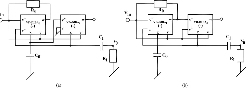
V+
V_
V+
V_ Z
Z V V
W W
C0
VD-DIBA1
(-) VD-DIBA2(-)
R0 V1
V2 I2 I1
(a)
V+
V_ V+
V_
Z
Z V V
W W
C0
VD-DIBA1
(-) VD-DIBA2(-)
R0 V1
V2 I2 I1
(b)
Figure 3. Proposed floating inductance simulation configu-rations.
On the other hand, analysis of the new FI circuits
shown in
Figures 3(a)
and
(b)
yields
1 2
2
1 1
2 0 2 0
1
1
1
, with
1
1
m m
m
g g
I
V
g
I
sC
V
R
(4)
which proves that the circuits simulate a floating lossless
inductance with the inductance value given by
1 2
0
eq
m m
C L
g g
(5)
The proposed CMOS implementation of VD-DIBA (
−
)
is shown in
Figure 4
. The CMOS VD-DIBA (
−
) is im-
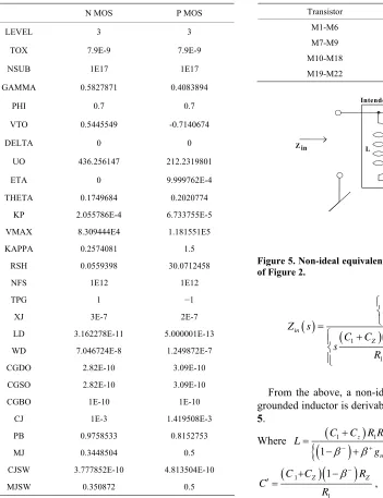
plemented using 0.35 µm MIETEC real transistor model
which are listed in
Table 1
. Aspect ratios of transistors
used are given in
Table 2
.
3. Non-Ideal Analysis and Sensitivity
Performance
Let
R
zand
C
zdenote the parasitic resistance and parasitic
capacitance of the Z-terminal. Taking into account the
non-idealities of the VD-DIBA (
−
), namely
w z
V
V
V
v, where
1
1
1 1
and
2 2 1
1are voltage tracking errors of the
VD-DIBA, for the circuit shown in
Figure 2
, the non-
1 M
10
M M11
3 M
13 M
12 M
14
M M16
5
M M6 M7
8 M
9 M
21 M 22
M 18
M 17
M M19 M20
15 M 2
M M4
VSS + V
-V
B
V1 VB2 VB3 VB4
V
Z
[image:3.595.62.536.94.219.2]W VDD
Figure 4. Proposed CMOS Implementation of VD-DIBA, VDD = −VSS = 2 V, VB1 = −0.44 V, VB2 = IB3 = −0.22 V and VB4 = −0.9
V.
Table 1.CMOS process parameters. Table 2.Dimensions of CMOS transistors.
N MOS P MOS
LEVEL 3 3
TOX 7.9E-9 7.9E-9
NSUB 1E17 1E17
GAMMA 0.5827871 0.4083894
PHI 0.7 0.7
VTO 0.5445549 -0.7140674
DELTA 0 0
UO 436.256147 212.2319801
ETA 0 9.999762E-4
THETA 0.1749684 0.2020774
KP 2.055786E-4 6.733755E-5
VMAX 8.309444E4 1.181551E5
KAPPA 0.2574081 1.5
RSH 0.0559398 30.0712458 NFS 1E12 1E12
TPG 1 −1
XJ 3E-7 2E-7
LD 3.162278E-11 5.000001E-13
WD 7.046724E-8 1.249872E-7
CGDO 2.82E-10 3.09E-10
CGSO 2.82E-10 3.09E-10
CGBO 1E-10 1E-10
CJ 1E-3 1.419508E-3
PB 0.9758533 0.8152753
MJ 0.3448504 0.5
CJSW 3.777852E-10 4.813504E-10
MJSW 0.350872 0.5
Transistor W/L (μm)
M1-M6 14/1 M7-M9 14/0.35 M10-M18 4/1 M19-M22 7/0.35
R'
C' R'' L
Intended
Parasitic
[image:3.595.305.538.275.505.2]Z in
Figure 5. Non-ideal equivalent circuit of grounded inductor of Figure 2.
1 1
1 1
1
1
1
z z in
Z m
Z
s C
C
R
Z
s
C
C
1
g
s
R
R R
R
(6)
From the above, a non-ideal equivalent circuit of the
grounded inductor is derivable which is shown in
Figure
5
.
Where
1
1 1
z Z
m Z
C
C
R R
L
g R
,
1
1
R
R
,
1
1
1
Z Z
C
C
R
C
R
[image:3.595.72.423.276.733.2]and
1 1 m Z
R R g R
From the above, the sensitivities of
L
with respect tovarious active and passive elements are found to be
0 0 1 1 1 , , 1 , 1 , 1 , 1 1 z z mL L z
C C z z L R m Z L m Z
L m Z
m Z
L m Z
g
m Z
C C
S S S
C C C C
S g R S g R g R S g R g R S g R
1, L R (7)
similarly, for the circuit shown in
Figures 3(a)
and
(b)
for
, the input-output currents and voltages
relationships are given by:
1
1 2 1 1 1 2 1 2 1 2 2 1 2 0 1 0 2 01
1
1
1
1
1 1
1
with
m m z Z z z Z Z m m mg g
I
I
s C
C
R
V
s C
C
sC
R
R
V
g g
g
R
(8)
The non-ideal equivalent circuit of floating inductors
of
Figures 3(a)
and
(b)
derivable from Equation (8) is
shown in
Figure 6
.
Where
1 2 0 1 m m
C
Cz
L
g g
and
1 1 2
1
z m m
R
R g g
The various sensitivities of
L
with respect to active andpassive elements are:
1
0 1 1
1 1
2
0
0 0
,
,
1,
0,
0
z m
m
z
L L L
C C g
z z
L L L
g
C
C
S
S
S
C
C
C
C
S
S
S
1,
(9)
Taking
g
m1
g
m2
389.673 A V
,
2,
1 2
z z
,
0and
0, these
sensitivities are found to be (1, 0, 1, 0, 0,
−
1) and (1, 0,
−
1,
−
1, 0, 0) for Equations (7) and (9) respectively. Thus,
1 0
z z
C
C
100 k
R
R
L R
Intended
Parasitic
Cz2
[image:4.595.314.526.89.237.2]Rz2
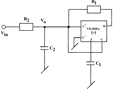
[image:4.595.89.283.147.321.2]Figure 6. Non-ideal equivalent circuit of floating inductor of Figure 3. V+ V_ Z V W C1 VD-DIBA (-) R1 Vin C2 R2 Vo
Figure 7. Band pass filter realized by the new grounded simulated inductor.
all the passive and active sensitivities of both grounded
and floating inductance circuits are low.
4. Simulation Results of the New Proposed
Grounded/Floating Inductance
Configurations
The workability of the proposed simulated inductors has
been verified by realizing a band pass filter (BPF) as
shown in
Figures 7
and
8
.
The transfer function realized by this configuration is
given by
1
2 2 0
2
2 2 1 2 1 1 1 m in
s
R C
V
g
V
s
s
R C
C C R
(10)
from where it is seen that bandwidth and centre fre-
quency are independently tunable, the former by
R
2 andthe latter by any of
R
1,
C
0.1 nFR
g
m1and
C
1. [image:4.595.329.514.280.427.2]1 2
2
1 2 1 2
1 0 0
1 0
2
0 0 1
1
with ,
m m
m
m m m m
in
R g g
s
C
V
g
R g g
g g
V
s
s
C
C C
R
(11)
simulated floating inductor (
Figure 10
) the inductance
value also remains constant up to 1 MHz.
[image:5.595.82.287.86.153.2]To verify the theoretical analysis of the application
circuits shown in
Figures 7
and
8
, they have also been
simulated using CMOS-based VD-DIBA (
−
) as shown in
Figure 4
. The component values used were for
Figure 7
:
C
1 = 0.1 nF,C
2 = 1 pF,R
1 = 100 kΩ
,
R
2 = 113.258 kΩ
and for
Figures 8(a)
and
(b)
:
C
0 = 0.1 nF,C
1 = 0.01 nF,R
0 = 100 kΩ
,
R
1 = 71.652 kΩ
,
m2(which
can be maintained by taking
V
B1 =−
1.5V). The VD-
DIBA was biased with ±2 volts D.C. power supplies with
V
B1 =−
0.44V,
V
B2 =V
B3 =−
0.22V and
V
B4=−
0.9V.
VD-DIBA (
−
) transconductance is controlled by
V
B1.Figure 11
,
Figures 12(a)
and
(b)
show the simulated fil-
ter responses of the BP filters.
In this case, bandwidth is tunable by
R
1 whereas centrefrequency can be tuned by
C
1.10 A V
g
Performance of the new simulated inductors was veri-
fied by SPICE simulations. CMOS-based VD-DIBA (
−
)
(as shown in
Figure 4
) was used to determine the fre-
quency responses of the grounded and floating simulated
inductors. The following values were used for grounded
inductor:
C
1 = 0.01nF,R
1 = 100 kΩ
,
1
m
and for the floating inductor:
C
0 =0 . 0 1 n F ,
R
0= 1 0 0 k
Ω
,
296.468 A Vg
1
m
,
The above described results, thus, confirm the validity
of the application of the proposed grounded and floating
simulated inductance circuits. A comparison of the vari-
ous salient features of the proposed configurations as
compared to other previous y known grounded and FI
296.468 A Vg
2
m
. From the frequency response of the
simulated grounded inductor (
Figure 9
) it has been ob-
served that the inductance value remains constant up to 1
MHz. Similarly, from the frequency response of the
10 A V
g
l
V+
V_
V+
V_ Z
Z V V
W W
C0
VD-DIBA1
(-) VD-DIBA2(-)
R0 Vin
R1 C1
V0 Vin
R1 C1
V0
V+
V_ V+
V_
Z
Z V V
W W
C0
VD-DIBA1
(-) VD-DIBA2(-)
R0
[image:5.595.88.511.345.498.2](a) (b)
Figure 8. Band pass filters realized by the new floating simulated inductors of Figures 3(a) and (b).
100 102 104 106 108 1010
-0.02 -0.015 -0.01 -0.005 0 0.005 0.01 0.015 0.02
Frequency (H)
Indu
ct
anc
e (
H
[image:5.595.147.447.524.719.2])
100 102 104 106 108 1010 -0.025
-0.02 -0.015 -0.01 -0.005 0 0.005 0.01 0.015 0.02 0.025
Frequency (Hz)
In
duc
ta
nc
e (
H
[image:6.595.153.444.88.273.2])
Figure 10. Frequency response of the simulated floating inductor.
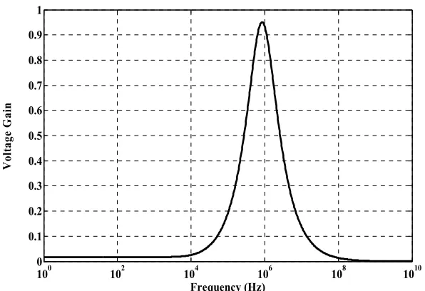
100 102 104 106 108 1010
0 0.1 0.2 0.3 0.4 0.5 0.6 0.7 0.8 0.9 1
Frequency (Hz)
Vo
lt
ag
e G
ai
[image:6.595.148.446.300.504.2]n
Figure 11. Frequency response of BPF using the proposed simulated grounded inductor.
100 101 102 103 104 105 106 107
0 0.1 0.2 0.3 0.4 0.5 0.6 0.7 0.8 0.9 1
Frequency (Hz)
V
olta
ge Gain
100 101 102 103 104 105 106 107
0 0.1 0.2 0.3 0.4 0.5 0.6 0.7 0.8 0.9 1
Frequency (H)
V
olt
ag
e Ga
im
(a) (b)
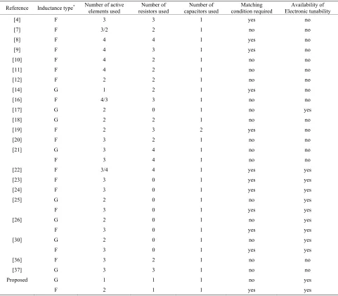
[image:6.595.61.538.536.711.2]Table 3.Comparison with other previously published grounded andfloating inductors.
Reference Inductance type* Number of active elements used
Number of resistors used
Number of capacitors used
Matching condition required
Availability of Electronic tunability
[4] F 3 3 1 yes no
[7] F 3/2 2 1 no no
[8] F 4 4 1 yes no
[9] F 4 3 1 yes no
[10] F 4 2 1 no no
[11] F 4 2 1 no no
[12] F 2 2 1 no no
[14] G 1 2 1 yes no
[16] F 4/3 3 1 no no
[17] G 2 0 1 no yes
[18] G 2 2 1 no no
[19] F 2 3 2 yes no
[20] F 3 2 1 no no
[21] G 3 4 1 no no
F 3 4 1 no no
[22] F 3/4 4 1 yes yes
[23] F 3 0 1 yes yes
[24] F 3 0 1 yes yes
[25] G 2 0 1 no yes
F 3 0 1 yes yes
[26] G 2 0 1 no yes
F 3 0 1 yes yes
[30] G 2 0 1 no yes
F 3 0 1 yes yes
[36] F 3 2 1 no no
[37] G 3 3 1 no no
Proposed G 1 1 1 no yes
F 2 1 1 yes yes
*F = Floating, G = Grounded.
simulators has been included in
Table 3
.
5. Conclusions
New circuits of lossless grounded and floating induc-
tance have been proposed employing VD-DIBAs. The
proposed grounded inductance circuit employs only one
VD-DIBA (
−
), one resistor and one grounded capacitor
and does not require any component matching condition.
On the other hand, the two floating inductance configu-
rations each using two VD-DIBAs (
−
), one resistor and
one grounded capacitor, need only a single realization
condition for floatation. The SPICE simulation results
have confirmed the workability of the new propositions
as well as the suggested application examples using them.
The problem of realizing any new single VD-DI-BA-
based FI configuration using a single grounded capacitor
and without requiring any matching condition appears to
be an interesting problem which is open to be investi-
gated.
6. Acknowledgements
The authors gratefully acknowledge Prof. Dr. Raj Senani,
Head, Division of Electronics and Communication
En-gineering, and Director NSIT, New Delhi, for useful dis-
cussions/suggestions.
REFERENCES
[1] R. Senani, “New Single-Capacitor Simulations of Float- ing Inductors,” Electro Component Science and Technol- ogy, Vol. 10, No. 1, 1982, pp. 7-10.
[2] A. Antoniou, “Gyrators Using Operational Amplifiers,” IEEE Electronics Letters, Vol. 3, No. 8, 1967, pp. 350- 352.
[3] A. Antoniou, “Realization of Gyrators Using Op-Amps and Their Use in RC Active Network Synthesis,” Pro- ceedings of the IEEE, Vol. 116, 1969, pp. 1838-1850. [4] R. Senani, “Realization of Single Resistance-Controlled
Lossless Floating Inductance,” IEEE Electronics Letters, Vol. 14, No. 25, 1978, pp. 828-829.
[5] T. S. Rathore and B. M. Singhi, “Active RC Synthesis of Floating Immittances,” International Journal of Circuit Theory and Applications, Vol. 8, No. 2, 1980, pp. 184- 188. doi:10.1002/cta.4490080212
[6] R. Senani, “Three Op-Amp Floating Immittance Simula- tors: A Retrospection,” IEEE Transactions on Circuits and Systems Part II, Vol. 36, No. 11, 1989, pp. 1463- 1465.
[7] R. Senani, “New Tunable Synthetic Floating Inductors,” IEEE Electronics Letters, Vol. 16, No. 10, 1980, pp. 382- 383.
[8] K. Pal, “Novel Floating Inductance Using Current Con- veyors,” IEEE Electronics Letters, Vol. 17, No. 18, 1981, p. 638.
[9] V. Singh, “Active RC Single-Resistance-Controlled Loss- less Floating Inductance Simulation Using Single Ground- ed Capacitor,” IEEE Electronics Letters, Vol. 17, No. 24, 1981, pp. 920-921.
[10] R. Senani, “Novel Lossless Synthetic Floating Inductor Employing a Grounded Capacitor,” IEEE Electronics Letters, Vol. 18, No. 10, 1982, pp. 413-414.
[11] W. Kiranon and P. Pawarangkoon, “Floating Inductance Simulation Based on Current Conveyors,” IEEE Elec- tronics Letters, Vol. 33, 1997, pp. 1748-1749.
[12] P. V. Anand Mohan, “Grounded Capacitor Based Grounded and Floating Inductance Simulation Using Current Con- veyors,” IEEE Electronics Letters, Vol. 34, No. 11, 1998, pp. 1037-1038.
[13] H. Sedef and C. Acar, “A New Floating Inductor Circuit Using Differential Voltage Current Conveyors,” Journal of RF-Engineering andTelecommunications, Vol. 54, No. 5-6, 2000, pp. 123- 125.
[14] E. Yuce, S. Minaei and O. Cicekoglu, “A Novel Grounded Inductor Realization Using a Minimum Number of Active and Passive Components,” ETRI Journal, Vol. 27, No. 4, 2005, pp. 427-432. doi:10.4218/etrij.05.0104.0149 [15] O. Cicekoglu, “Active Simulation of Grounded Inductors
with CCII+s and Grounded Passive Elements,” Interna- tional Journal of Electronics, Vol. 85, No. 4, 1998. pp. 455-462. doi:10.1080/002072198134003
[16] E. Yuce, “On the Realization of the Floating Simulators Using Only Grounded Passive Components,” Analog In- tegrated Circuits and Signal Processing, Vol. 49, 2006, pp. 161-166. doi:10.1007/s10470-006-9351-7
[17] T. Parveen and M. T. Ahmed, “Simulation of Ideal Grounded Tunable Inductor and Its Application in High Quality Multifunctional Filter,” Microelectronics Journal, Vol. 23, No. 3, 2006, pp. 9-13.
doi:10.1108/13565360610680703
[18] A. Fabre, “Gyrator Implementation from Commercially Available Trans Impedance Operational Amplifiers,” IEEE Electronics Letters, Vol. 28, No. 3, 1992, pp. 263-264. [19] R. Senani and D. R. Bhaskar, “New Lossy/Lossless Syn-
thetic Floating Inductance Configuration Realized with Only Two CFOAs,” Analog Integrated Circuits and Sig- nal Processing, Vol. 73, No. 3, 2012, pp. 981-987. doi:10.1007/s10470-012-9897-5
[20] R. Senani and J. Malhotra, “Minimal Realizations of a Class of Operational Mirrored Amplifier Based Floating Impedance,” IEEE Electronics Letters, Vol. 30, No. 14, 1994, pp. 1113-1114.
[21] K. Pal and M. J. Nigam, “Novel Active Impedances Us- ing Current Conveyors,” Journal of Active and Passive Electronic Devices, Vol. 3, No. 1, 2008, pp. 29-34. [22] A. U. Keskin and H. Erhan, “CDBA-Based Synthetic
Floating Inductance Circuits with Electronic Tuning Pro- perties,” ETRI Journal, Vol. 27, No. 2, 2005, pp. 239-242. doi:10.4218/etrij.05.0204.0055
[23] W. Tangsrirat and W. Surakampontorn, “Electronically Tunable Floating Inductance Simulation Based on Current- Controlled Current Differencing Buffered Amplifiers,” Thammasat International Journal of Science and Tech- nology, Vol. 11, No. 1, 2006, pp. 60-65.
[24] D. Biolek and V. Biolkova, “Tunable Ladder CDTA- Based Filters,” 4th Multi Conference (WSEAS), Spain, 19-21 December 2003, pp. 1-3.
[25] D. Prasad, D. R. Bhaskar and A. K. Singh, “New Ground- ed and Floating Simulated Inductance Circuits Using Current Differencing Transconductance Amplifiers,” Ra- dio Engineering Journal, Vol. 19, No. 1, 2010, pp. 194- 198.
[26] R. Nandi, “Lossless Inductor Simulation: Novel Configu- rations Using DVCCs,” IEEE Electronics Letters, Vol. 16, No. 17, 1980, pp. 666-667.
[27] M. T. Abuelmaatti, M. H. Khan and H. A. Al-Zaher, “Si- mulation of Active-Only Floating Inductance,” Journal of RF-Engineering and Telecommunications, Vol. 52, No. 7-8, 1998, pp. 161- 164.
[28] D. Biolek, R. Senani, V. Biolkova and Z. Kolka, “Active Elements for Analog Signal Processing; Classification, Review and New Proposals,” Radioengineering, Vol. 17, No. 4, 2008, pp. 15-32.
[29] D. Biolek and V. Biolkova, “First-Order Voltage-Mode All-Pass Filter Employing One Active Element and One Grounded Capacitor,” Analog Integrated Circuits and Signal Processing, Vol. 65, No. 1, 2010, pp. 123-129. [30] D. Prasad, D. R. Bhaskar and K. L. Pushkar, “Realization
of New Electronically Controllable Grounded and Float- ing Simulated Inductance Circuits using Voltage Differ- encing Differential Input Buffered Amplifiers,” Active and Passive Electronic Components, 2011, Article ID 101432.
[31] D. Prasad, D. R. Bhaskar and K. L. Pushkar, “Electroni- cally Controllable Sinusoidal Oscillator Employing CMOS VD-DIBAs,” ISRN Electronics, Vol. 2013, Article ID 823 630, 6 Pages. doi:10.1155/2013/823630
Mode Universal Biquad Filter Employing Single Voltage Differencing Differential Input Buffered Amplifier,” Cir- cuits and Systems, Vol. 4, No. 1, 2013, pp. 44-48. doi:10.4236/cs.2013.41008
[33] K. L. Pushkar,D. R. Bhaskar and D. Prasad, “A New MISO-Type Voltage-Mode Universal Biquad Using Sin- gle VD-DIBA,” ISRN Electronics, Vol. 2013, Article ID: 478213, 5 Pages. doi:10.1155/2013/478213
[34]R. Senani, “Some New Synthetic Floating Inductance Cir- cuits,” AEU: International Journal of Electronics and Communications, Vol. 35, 1981, pp. 307-310.
[35] R. Senani, “Canonic Synthetic Floating-Inductance Cir-
cuits Employing Only a Single Component-Matching Condition,” Journal of IETE, Vol. 27, No. 6, 1981, pp. 201-204.
[36] S. A. Al-Walaie and M. A. Alturaigi, “Current Mode Si- mulation of Lossless Floating Inductance,” International Journal of Electronics, Vol. 83, No. 6, 1997, pp. 825-830. doi:10.1080/002072197135094